Review

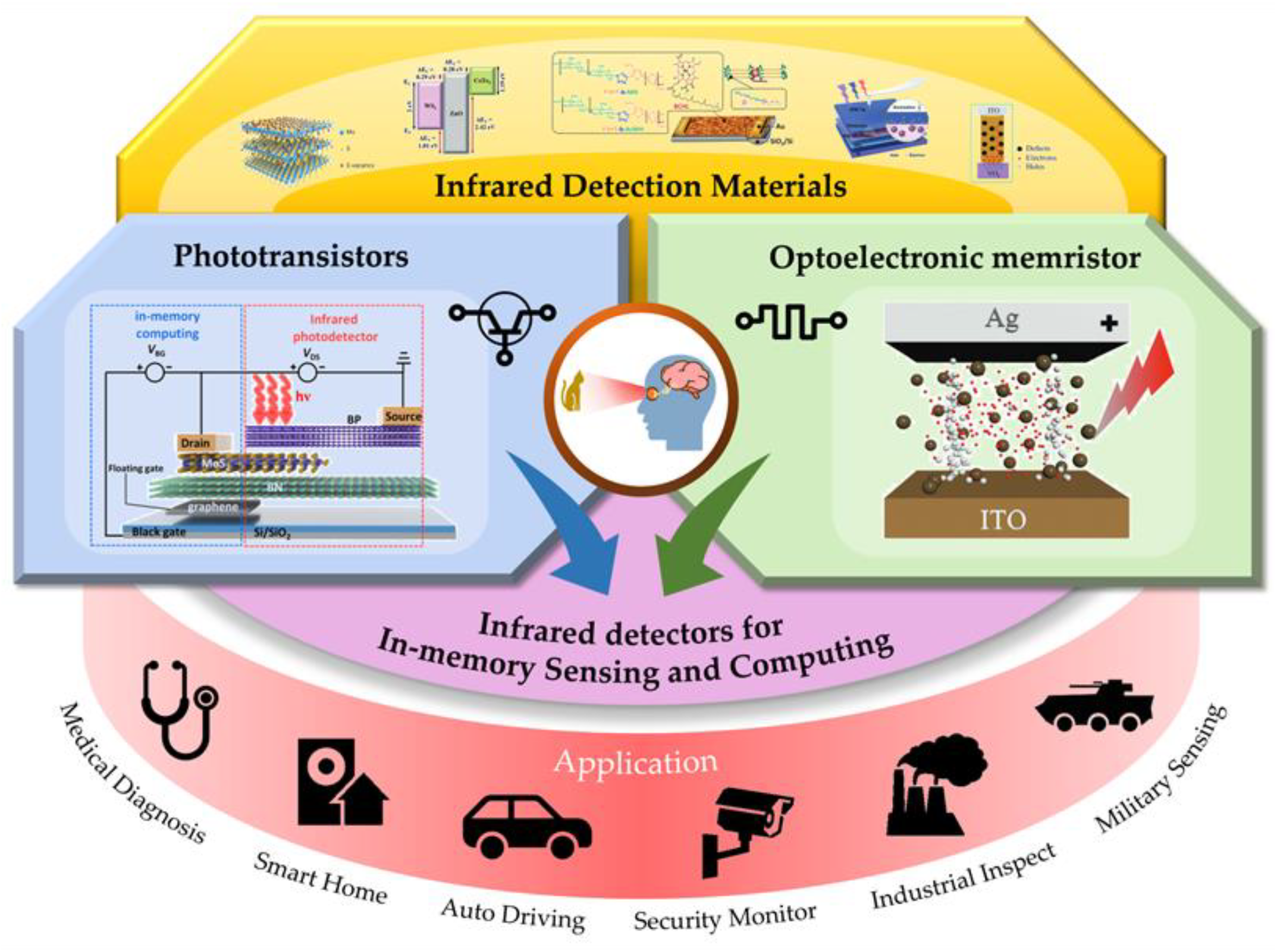
Advances in Infrared Detectors for In-Memory Sensing and Computing

1
School of Optics and Photonics, Beijing Institute of Technology, Beijing 100081, China
2
Yangtze Delta Region Academy of Beijing Institute of Technology, Jiaxing 314019, China
*
Authors to whom correspondence should be addressed.
These authors contributed equally to the work.
Photonics 2024, 11(12), 1138; https://doi.org/10.3390/photonics11121138
Submission received: 7 November 2024 / Revised: 28 November 2024 / Accepted: 2 December 2024 / Published: 3 December 2024
(This article belongs to the Special Issue Organic Photodetectors, Displays, and Upconverters)

Abstract

:
In-memory sensing and computing devices integrate the functionalities of sensors, memory, and processors, offering advantages such as low power consumption, high bandwidth, and zero latency, making them particularly suitable for simulating synaptic behavior in biological neural networks. As the pace of digital transformation accelerates, the demand for efficient information processing technologies is increasing, and in-memory sensing and computing devices show great potential in AI, machine learning, and edge computing. In recent years, with the continuous advancement of infrared detector technology, infrared in-memory sensing and computing devices have also seen new opportunities for development. This article reviews the latest research progress in infrared in-memory sensing and computing devices. It first introduces the working principles and performance metrics of in-memory sensing and computing devices, then discusses in detail transistors and memristor-type devices with infrared band response, and finally looks forward to the development prospects of the field. Through innovation in new semiconductor materials and structures, the development trajectory of infrared in-memory sensing and computing devices has been significantly expanded, providing new impetus for the development of a new generation of information technology.

1. Introduction

With the acceleration of global digital transformation, the demand for technologies capable of efficiently processing large volumes of data and responding instantaneously has surged dramatically, making the limitations of the traditional von Neumann architecture increasingly apparent. From the late 20th to the early 21st century, the rapid development of the Internet of Things (IoT) and big data technologies has intensified the need for large-scale parallel computing and efficient data transmission, thereby highlighting the “memory wall” problem in conventional architectures [1,2]. Inspired by the human visual system, known for its robust visual perception and information processing capabilities, researchers began exploring new devices that integrate sensing, storage, and computing functionalities on a single chip. In 2008, memristors—electronic components with memory properties—were invented [3]. Subsequently, the application of innovative devices such as photonic memristors and transistor synapses further advanced the field [2,4,5]. These devices combine the roles of sensors, memory, and processors, enabling localized data processing. They possess characteristics such as low power consumption, high bandwidth, and negligible latency [6], making them particularly well-suited for emulating synaptic behaviors in biological neural networks. Additionally, in-memory sensing and computing (ISC) devices exhibit excellent plasticity and adaptability, allowing them to dynamically adjust their states in response to environmental stimuli. These attributes present vast potential for their use in efficient and intelligent systems.
Currently, ISC devices hold a significant position in several cutting-edge technological domains. Firstly, in the fields of artificial intelligence (AI) and machine learning (ML), ISC devices significantly enhance the speed and accuracy of algorithm training by performing key operations directly at the hardware level, such as convolutional operations and matrix multiplications [7,8], thus reducing data transfer overhead, accelerating model iteration, and fostering the in-depth development of AI technology. Secondly, ISC devices are crucial in edge computing [9]. Their compact design and efficient energy utilization meet the balancing needs of intelligent terminal devices between complex computational tasks and low-power operation, enhancing the level of intelligence in smart homes, industrial automation, and other sectors. In the context of biomedical engineering, ISC devices used in portable medical monitoring devices [10] enable continuous monitoring and real-time analysis of human physiological parameters. By processing data locally, they mitigate security risks and protect personal privacy by avoiding frequent data uploads to the cloud. Furthermore, in complex and dynamic autonomous decision-making scenarios such as autonomous driving [11,12], ISC devices enhance system safety and reliability through powerful image recognition and rapid response capabilities.
The application of ISC devices in infrared detection technology is particularly noteworthy. Infrared radiation, situated between visible light and microwaves, possesses unique characteristics such as penetrability, temperature sensitivity, and atmospheric transmission windows. It can penetrate materials opaque to visible light, providing clear imaging under low-visibility conditions. Additionally, the wavelength of infrared radiation emitted by objects reflects their temperature characteristics, making infrared detection technology suitable for non-contact temperature measurement and thermography [13]. The effective atmospheric transmission window of infrared radiation makes it an ideal choice for communication and imaging, which is particularly beneficial in ISC devices. These characteristics render infrared information perception technology widely applicable in night vision, remote sensing monitoring, medical diagnosis, industrial inspection, military reconnaissance, autonomous driving, and security surveillance [14], among other areas. With the growing demand for optoelectronic detection, the need for intelligent perception of infrared information is becoming increasingly urgent.
However, among reported ISC devices and artificial vision systems, devices operating in the visible and ultraviolet light bands dominate, while research on the infrared band remains relatively sparse [15,16]. The evolution of infrared detector technology is intrinsically linked to the advancement of ISC devices, as the former provides the foundational capabilities that enable the latter to achieve enhanced performance and integration in infrared optoelectronic systems. The drawbacks of traditional infrared detectors, such as difficulties in molecular epitaxial growth and incompatibility with memristor fabrication processes [17], hinder the development of compact integrated systems, thereby limiting the advancement of infrared optoelectronic memristors. Nevertheless, recent advancements in artificial microstructures, bandgap engineering [18], and novel semiconductor material applications [19] have ushered in the third generation of infrared detector development [20], leading to progress in low-cost, high-performance, large-array infrared detectors [21,22,23,24,25]. As these technologies evolve, ISC devices exhibiting good infrared band response have also made significant breakthroughs.
A review of the literature highlights the significant attention attracted by the development of ISC devices in recent years. Specifically, in 2024, Huang et al. [26] provided an insightful overview of the research advancements in the device principles and applications of bio-inspired visual systems based on photonic synapses. Building on this foundation, Hu et al. [16] further explored the emerging optoelectronic neuromorphic devices designed for brain-like computing, encompassing artificial synapses based on memristors and transistors, as well as a variety of photonic neurons. They proposed a development pathway aimed at extending the response wavelength range through the use of narrow-bandgap materials.
Moreover, the application of novel low-dimensional materials and structures in infrared detectors has seen rapid advancement in recent years. Zhang et al. [27] conducted a comprehensive review of the development of photothermal sensing systems based on nanomaterials, with a focus on the utilization of inorganic, organic, and composite photothermal nanomaterials in sensing technologies. In parallel, Zhu et al. [28] concentrated on black phosphorus materials, detailing the performance and characteristics of various types of infrared photonic detectors based on different structures of two-dimensional black phosphorus. The enhanced optoelectronic performance of these black phosphorus-based structures has enabled a wide range of infrared light detection applications across the NIR (near-infrared), SWIR (short-wave infrared), and MIR (mid-infrared) regions.
These research directions have clearly gained significant traction, indicating a positive trend in the development of ISC devices and the next generation of infrared detectors. Continuous innovations in infrared detection materials and structures have significantly broadened the development pathways for integrated ISC devices. Figure 1 illustrates the development elements of infrared ISC devices. However, there remains a need for a systematic summary and review of the research findings on ISC devices with infrared band response characteristics. A comprehensive organization of these research results would undoubtedly facilitate deeper and broader development in this field.
Therefore, this paper focuses on the research outcomes of infrared ISC devices. We first introduce the working principles and performance metrics of ISC devices, then discuss transistors and memristor-type devices with infrared band response, and finally provide an outlook on the field’s development. We believe that this paper will serve as an essential reference for future research in this domain, promoting the ongoing development and innovation of infrared ISC devices.

2. Performance of ISC Devices

2.1. Working Principles of ISC Devices

ISC devices (also known as in-storage computing or processing-in-memory) function similarly to the working principles of neurons and synapses in biological neural networks, particularly in how they efficiently process information [1]. In the human brain, neurons form complex networks through synaptic connections that can perform tasks such as learning, memory, and computation. These processes are highly parallelized and extremely energy-efficient. In neuromorphic computing, artificial synaptic devices mimic the signal transmission process in biological synapses through specific electronic or optoelectronic properties [36,37], primarily consisting of two types of components: two-terminal memristors and three-terminal transistors. These two structures have distinct working mechanisms and characteristics.
Memristors, as the fourth two-terminal element following resistors, capacitors, and inductors, were first proposed by Leon Chua and others in 1971 [38]. The uniqueness of memristors lies in their ability to change their resistance value based on the history of charge passing through them, and this change can be maintained even after power is cut off, endowing them with non-volatile memory capabilities [39]. This allows memristors not only to store information like traditional hard drives but also to have the advantages of smaller size and faster read–write speeds. By changing the voltage or current applied to them, the resistance state of memristors can be adjusted, achieving a transition from a high-resistance state to a low-resistance state, making them an ideal choice for simulating biological synapses and neurons in artificial neural networks [39,40]. In the field of optoelectronic integration, photosensitive material-based photonic memristors show unique advantages. These devices use specific mechanisms to convert property changes caused by light exposure into changes in electrical conductivity, thereby achieving the function of integration of sensing, storage, and computing [41]. Depending on the working mechanism of the photosensitive materials, photonic memristors can be classified into photon–ion coupled type, photon–electron coupled type, ferroelectric type, and phase change type, among others [40].
Two-terminal memristors simulate synaptic functions by directly corresponding to the pre-synaptic and post-synaptic terminals with two electrodes. In these devices, resistive switching effects are commonly used to mimic long-term potentiation (LTP) or long-term depression (LTD) phenomena. When specific forms of electrical or optical signals are applied to the memristor, the internal density of oxygen vacancies or other defect states will change accordingly, leading to an increase or decrease in resistance value, thereby adjusting synaptic weights. The active layer, located between the upper and lower electrodes, responds to external stimuli through its own physicochemical properties and changes its conductivity based on different stimulation conditions, thereby simulating the role of neurotransmitters [15,42]. This approach not only simplifies the design of artificial neural networks but also enhances system efficiency and flexibility.
In 1996, researchers first used transistors to simulate the learning function of synapses [43]. As a semiconductor device that can amplify current or act as a switch, the working principle of a transistor is to control the current flow between the source and drain through gate voltage control. In three-terminal optoelectronic synaptic transistors, there is a significant correspondence with biological synapses: the source and drain of the transistor represent the pre-synaptic membrane (sending information) and post-synaptic membrane (receiving information), respectively, while the process of current flowing from the source to the drain is similar to neurotransmitters being released from the pre-synaptic terminal and acting on the post-synaptic terminal [5,15]. The gate of the transistor is used to regulate the conduction state between the source and drain. In artificial synapse design, synaptic weights can be adjusted by changing the gate voltage, thereby mimicking synapses of varying strengths [5].
When using optical pulses as external stimuli, they can affect the distribution of carriers within the gate region, thereby adjusting the conductivity of the device. This mechanism is similar to the changes in synaptic efficacy caused by changes in calcium ion concentration in biological synapses [37]. Additionally, the active material between the source and drain is equivalent to the synaptic cleft, which contains movable carriers that can be regarded as neurotransmitters. External stimuli such as light exposure can cause changes in the carrier density within the active material, leading to corresponding changes in conductivity, generating excitatory post-synaptic current/potential (EPSC/EPSP) or inhibitory post-synaptic current/potential (IPSC/IPSP) [5,37].

2.2. Performance Indicators

Plasticity evaluation is one of the key indicators for synaptic devices, reflecting the device’s ability to mimic the learning and memory functions of biological nervous systems. In optoelectronic synaptic devices, plasticity is typically divided into Short-Term Plasticity (STP) and Long-Term Plasticity (LTP), which correspond to short-term memory (STM) and long-term memory (LTM) respectively [44].
Short-Term Plasticity includes Paired-Pulse Facilitation (PPF) and Paired-Pulse Depression (PPD). PPF refers to the phenomenon where the response to the second of two consecutive stimuli is stronger than the first [45], while PPD is the opposite, showing a weakened response after the second stimulus. These effects allow artificial neural networks to adjust their responses based on previous stimuli, achieving dynamic regulation in information processing. STP can be simulated by applying rapid consecutive electrical or optical pulses and characterized by measuring the changes in excitatory postsynaptic current (EPSC) caused by the second pulse compared to the first [46]. Additionally, changing the interval between pulses can further investigate short-term memory effects.
Long-Term Plasticity involves a more enduring memory formation process. LTP can be induced by sustained or repeated application of specific patterns of stimulation, such as high-frequency pulse sequences, leading to a lasting increase in synaptic weights. In experiments, LTP is verified by recording the conductance state after a series of trainings and checking whether this state can be maintained for a longer period. Moreover, by adjusting the intensity of the optical pulses used to induce STM, a smooth transition between STM and LTM can be achieved. As the number of optical pulses increases, EPSC will slowly rise and gradually decay, which is a sign of LTM formation. If the stimulation is strong enough, some carriers may be captured in deep defects of the material, preventing conductivity from fully returning to its initial state, thus simulating the transition from working memory to long-term storage [15,47].
Spike-Timing-Dependent Plasticity (STDP), as a learning rule for LTP, has been successfully simulated in optoelectronic synaptic memristors. STDP adjusts the synaptic weight based on the relative timing difference between pre-synaptic and post-synaptic spikes. When a pre-synaptic spike arrives before a post-synaptic spike, the synaptic weight increases, leading to LTP. Conversely, if a post-synaptic spike precedes a pre-synaptic spike, the synaptic weight decreases, resulting in LTD [37,47]. The STDP mechanism is crucial for associative learning and sequence learning, enabling neural networks to recall original patterns even when faced with incomplete or noisy inputs. Additionally, it allows the network to predict future events based on the temporal sequence of previous events.
In addition to STDP, Spike-Rate-Dependent Plasticity (SRDP) is another significant learning principle that modulates synaptic weights by altering the firing rate of pre-synaptic neurons. Specifically, low-frequency firing typically leads to LTD, while high-frequency firing triggers LTP [5]. SRDP highlights activity-dependent synaptic plasticity, indicating that lower (higher) post-synaptic activity reduces (enhances) synaptic efficacy. This mechanism primarily focuses on adjusting synaptic weights by controlling the firing frequency of pre-synaptic neurons.
In addition to plasticity, there are several other key characterization parameters that are crucial for evaluating the overall performance of synaptic electronic devices. Retention characteristics refer to the length of time a device can maintain a specific resistance state without external stimulation. This is essential for memory functions, and good retention characteristics mean that information can be saved for a long time without loss. In neuromorphic computing and storage applications, retention characteristics are one of the key indicators for evaluating the long-term stability of devices. They directly affect the persistence and reliability of data [48]. For ISC devices, retention characteristics determine their ability to reliably store and process information over time, supporting complex cognitive tasks. This can be assessed by long-term tracking and observation of stored information, recording its changes over time.
The on/off ratio refers to the ratio of the resistance when the device is in the conductive state to the resistance when it is in the disconnected state. A high on/off ratio indicates a more distinct difference between the two states, which helps reduce the possibility of misreading and can lower energy consumption [48,49]. A high on/off ratio is crucial for achieving clear data differentiation and accurate information processing, especially in applications requiring precise control of weight updates. It can be measured by recording the resistance values of the device in the high-resistance state and the low-resistance state, then calculating their ratio.
Endurance refers to how many write–erase cycles an optoelectronic memristor can withstand before it can no longer function properly. This is an important indicator for evaluating its long-term stability, especially in storage applications [48,49]. High endurance means that the device can maintain its performance after multiple operations, which is crucial for long-term storage devices and computing systems. Endurance directly affects the reliability and service life of the system, especially in application scenarios requiring frequent data updates. It is assessed by repeatedly performing SET-RESET operations and monitoring changes in device performance. The memristor is repeatedly switched between the high-resistance state (HRS) and the low-resistance state (LRS). This is usually achieved by applying a positive or negative voltage pulse. Specific parameters (such as voltage amplitude, pulse width) should be adjusted according to device characteristics.
Energy consumption mainly focuses on the amount of energy required to perform various operations such as changing states and reading information. Low energy consumption is not only beneficial for extending battery life but also particularly important in large-scale integrated systems. Low energy consumption is one of the key advantages of in-memory sensing and computing devices, especially in edge computing and portable devices. Low energy consumption helps improve the overall energy efficiency of the system, reduce heat generation, extend battery life, and thus support longer operation times. It is usually quantified by measuring the energy required for a single pulse event, such as the energy consumption per synaptic event.
Linearity reflects whether the device’s response to input signals of different intensities is linearly related. Good linearity is crucial for accurate signal processing and weight updates. Linearity is essential for ensuring the accuracy of signal processing, especially in applications requiring precise control of weight updates [50]. Good linearity helps simplify the design of models and algorithms, enhancing the overall performance of the system. It is usually tested by applying a series of stimuli of different intensities and recording the corresponding output changes.
In summary, plasticity, retention characteristics, on/off ratio, endurance, energy consumption, and linearity are important indicators for evaluating the performance of synaptic electronic devices. These parameters together determine the reliability and effectiveness of devices in practical applications, providing a foundation for designing high-performance neuromorphic computing systems.

3. Development of Infrared ISC Devices

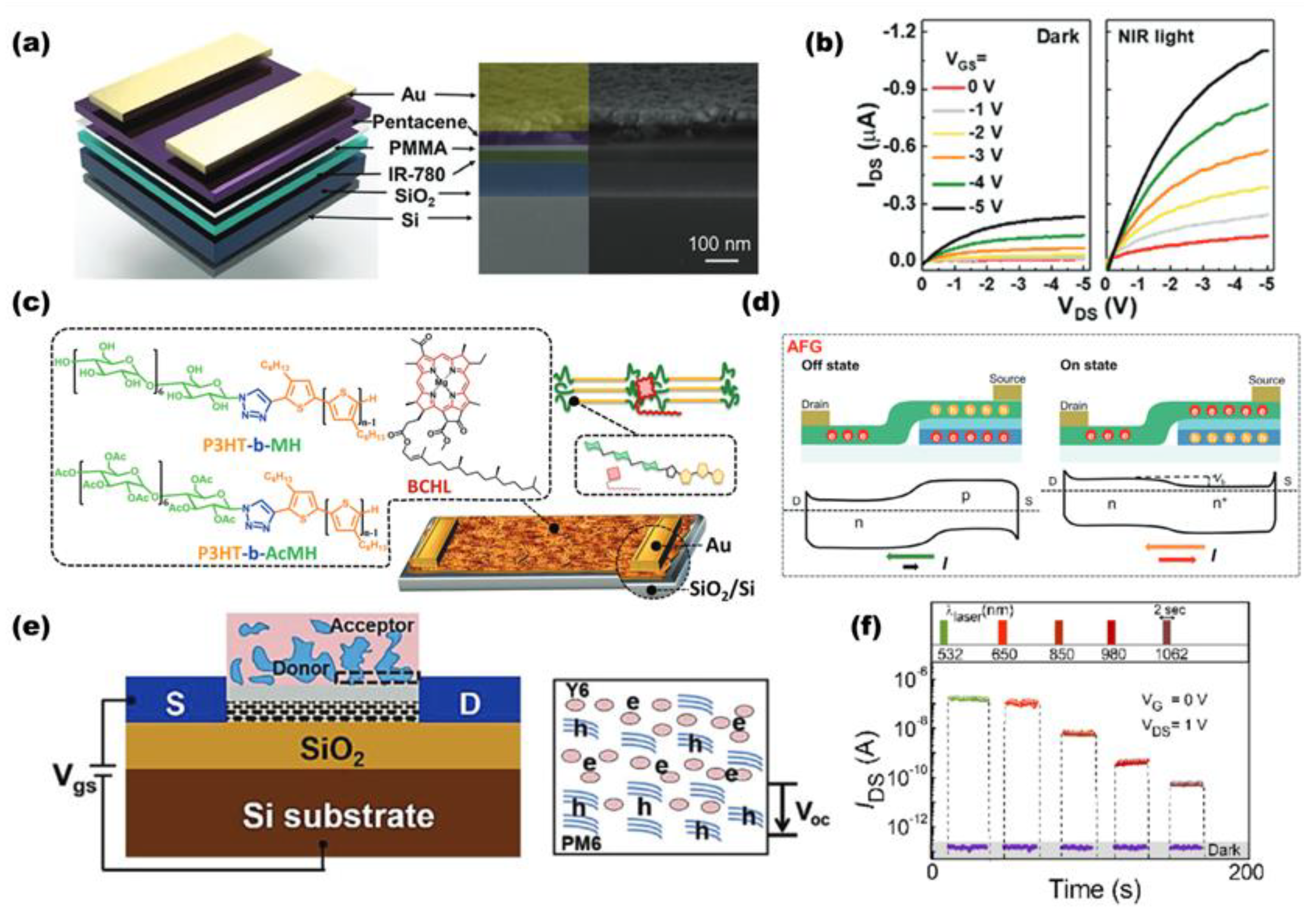
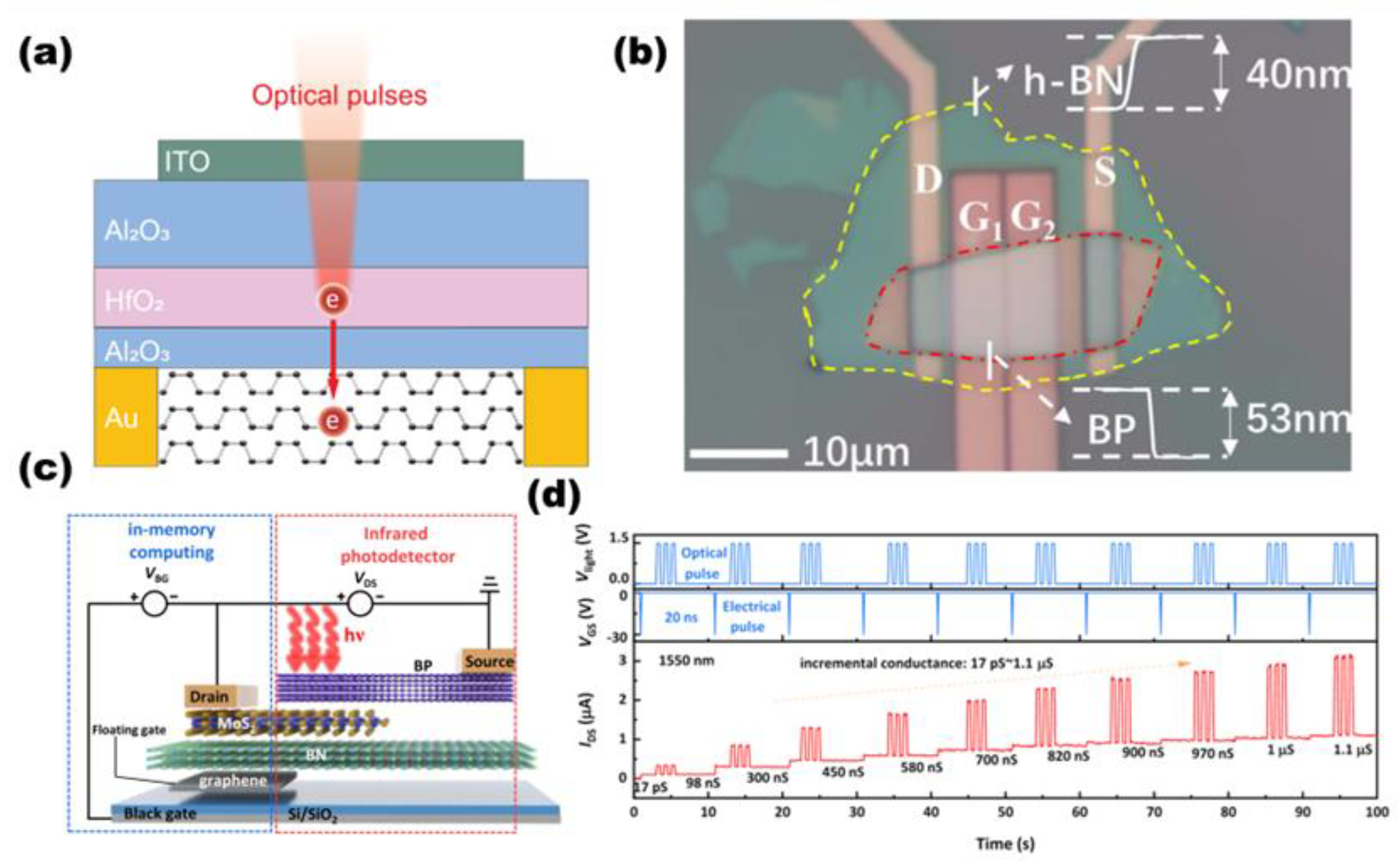
3.1. Phototransistors for Storage and Computation

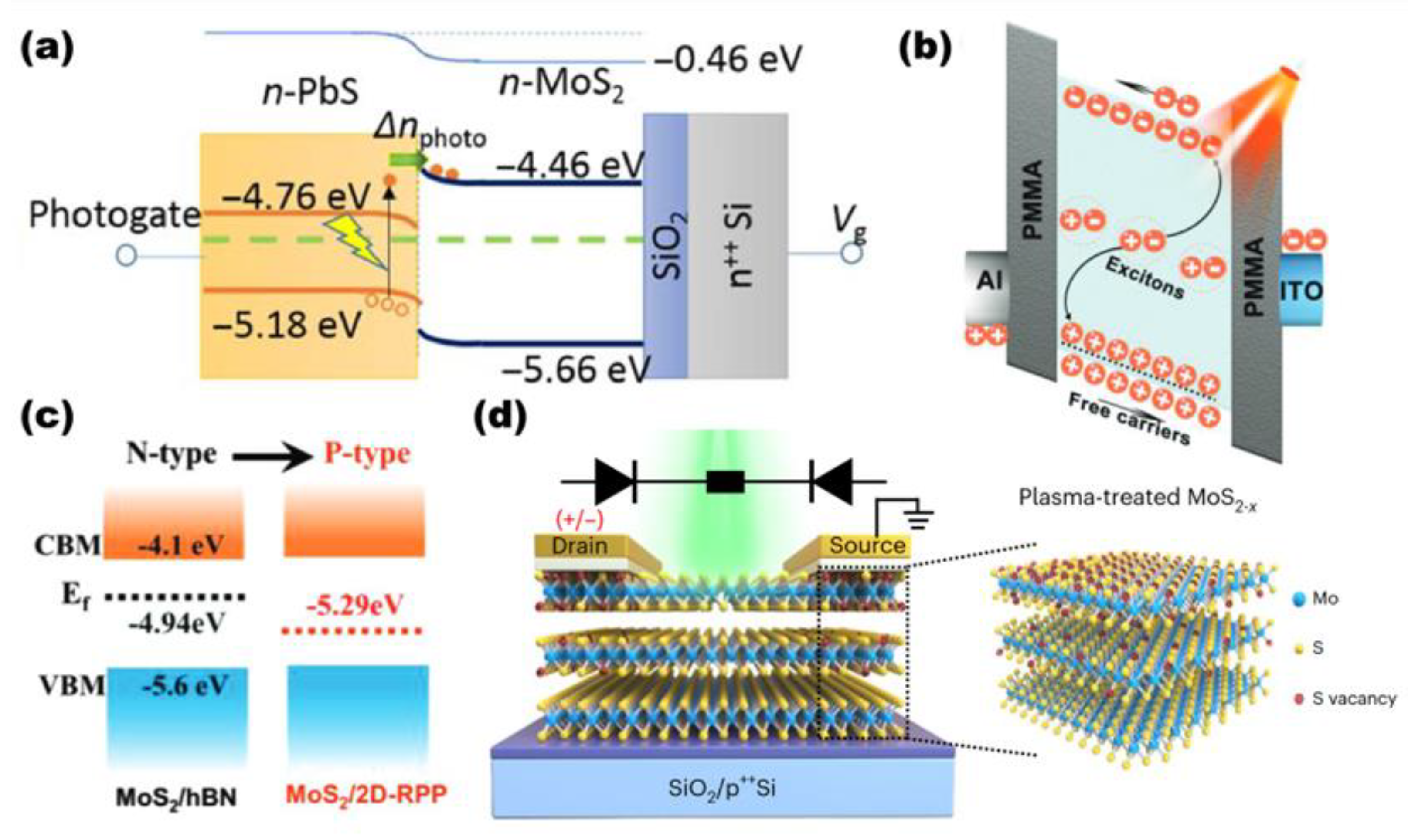
3.1.1. Heterojunction Transistors

Heterojunction transistors utilize the heterojunction structure between different materials to achieve photoelectric response and storage functions. These transistors are typically composed of two or more materials. Under illumination, photogenerated electron–hole pairs are generated and separated at the heterojunction, thereby changing the conductivity of the material. This structure not only enables efficient photoelectric conversion but also allows the control of the device’s electrical conductivity state by adjusting the intensity and duration of light exposure, realizing storage and computational functions [5].
Transition metal dichalcogenides (TMDs) MX2 (where M = Mo, W; X = S, Se) have attracted significant attention for their exceptional performance in infrared detection [51]. These materials possess a bandgap ranging from approximately 1.4 eV to 2.0 eV, covering the visible to near-infrared (NIR) region, which is crucial for infrared detectors. For instance, the bandgap of monolayer MoSe2 is approximately 1.413 eV, and that of monolayer WSe2 is approximately 1.444 eV. These bandgap values enable them to absorb infrared light and convert it into electrical signals. TMDs also exhibit strong exciton effects with exciton binding energies reaching dozens of meVs; for example, the exciton binding energies of MoSe2 and WSe2 are around 30 meV, enhancing their light absorption and emission efficiencies in the infrared band. Additionally, the bandgap of TMDs can be adjusted via strain engineering. Experiments have demonstrated that a strain of 1% can lead to a bandgap change of about 300 meV. This strain sensitivity provides an effective means of tuning the spectral response of detectors. Therefore, TMDs demonstrate great potential in infrared detection applications due to their tunable bandgap, strong exciton effects, and strain controllability.
In 2020, Wang et al. [52] designed and synthesized a phototransistor based on MoSe2/Bi2Se3 heteronanosheets. The device structure is shown in Figure 2a. By leveraging the charge transfer effect between MoSe2 and Bi2Se3, they formed an effective heterojunction, enhancing the light absorption capability and charge capture dynamics. Under NIR light illumination at 790 nm, the heterojunction phototransistor exhibited a significant enhancement in responsivity by a factor of 440 and detectivity by a factor of 200. Furthermore, by modulating the intensity and frequency of the light, the precision of image recognition could be adjusted, achieving a recognition rate as high as 90%. In 2023, Yang et al. [53] reported a near-infrared optical synaptic device based on a multilayer MoSe2 moiré superlattice for artificial retina applications. By designing a multilayer MoSe2 moiré superlattice structure, the study significantly enhanced interlayer coupling, achieving broadband absorption from 240 nm to 1700 nm, particularly in the NIR region. Figure 2b,c illustrates the mechanism of the multilayer MoSe2 superlattice synaptic device. Selenium vacancies in the MoSe2 moiré superlattice endowed the device with basic synaptic performance. The exciton enhancement due to van der Waals interactions between MoSe2 layers brought the bandgap close to that of the bulk material, enabling a response to NIR light. This study constructed a 10 × 10 integrated retina-like device array, maintaining a memory level of 14.84% even after 50 s of decay under 1060 nm light pulse stimulation, reflecting excellent storage function under NIR lighting conditions. This research opens new avenues for realizing NIR artificial retinas and bionic eyes based on two-dimensional materials. In 2024, Hou et al. [54] designed and implemented an infrared artificial visual synaptic device based on a p-WSe2/n-Ta2NiS5 van der Waals heterojunction. The innovation lies in the heterostructure formed by p-type WSe2 and n-type Ta2NiS5, allowing self-powered infrared light detection through the built-in electric field and photonic synaptic functionality via bias-induced band bending. This heterojunction successfully mimicked synaptic behavior, extending the sensing wavelength to the infrared region (1064 and 1550 nm) with PPF values reaching 23% and 100%, respectively. Additionally, by adjusting the width, interval, number, and intensity of the light pulses, the infrared synaptic behavior was thoroughly investigated, and a 3 × 3 visual image array was demonstrated to showcase the potential for image perception, memory, and application in information filtering and dynamic capture. Figure 2d illustrates the band structure of the p-WSe2/n-Ta2NiS5 van der Waals heterojunction and the corresponding changes, explaining how the heterojunction’s band alignment shifts from type II to type III under bias-free and biased conditions, which is critical for understanding the photonic behavior of the device in different operational modes.
Molybdenum disulfide (MoS2), as a two-dimensional transition metal dichalcogenide with a direct bandgap, has attracted significant attention due to its outstanding performance in the field of infrared detection. The bandgap of MoS2 increases with the reduction of layers, especially at the monolayer limit, where it can reach 1.8 eV, making it strongly absorbent to visible to near-infrared light. MoS2’s high absorption coefficient can reach 106/cm, far exceeding that of traditional semiconductors like silicon and gallium arsenide, enabling the construction of highly efficient photodetectors based on extremely thin material layers. Additionally, MoS2’s carrier mobility can reach 200 cm2/(V·s), ensuring rapid signal response. In infrared detection applications, MoS2-based photodetectors exhibit characteristics of high sensitivity, fast response, and low dark current. By combining with materials such as quantum dots and graphene, the performance of MoS2 detectors can be further enhanced, broadening their spectral response range and increasing photocurrent gain [55].
In 2019, Kim et al. [56] proposed a germanium-gated MoS2 phototransistor, which achieved a broad detection range from visible light to infrared (520 to 1550 nm). Using germanium as the gate material, the MoS2 photoelectric device was able to mimic the potentiation and depression behaviors of neural synapses under illumination at wavelengths of 520 nm and 1550 nm, thereby demonstrating the functionality of a multilevel optical-neuromorphic device. Under experimental conditions, the MoS2 phototransistor exhibited a high responsivity of 4.5 × 10⁴ A/W in the infrared band and also showed significant performance in the visible light range. Additionally, the device demonstrated a non-overlapping current range under different light conditions, which is crucial for developing photoelectric devices that integrate sensing and computing functions, especially those that need to operate under complex ambient lighting conditions. This study not only expanded the application range of the two-dimensional material MoS2 but also provided a new direction for the design of future artificial synapses, particularly in simulating the functions of biological synapses. Similarly, Islam et al. [57] employed PtTe2/Si, which is sensitive to infrared light, in conjunction with gate electrodes, enabling the device to respond to light ranging from 300 nm ultraviolet to 2 μm infrared. The design not only broadened the photoreceptive spectrum of the optoelectronic synapse but also achieved synaptic weight updates for multi-wavelength light through short-term and long-term synaptic plasticity controlled by optical stimulation. Furthermore, the research demonstrated the capability of recognizing single-wavelength and mixed-wavelength patterns using extracted synaptic weight update parameters in artificial neural network simulations. This provides new insights into the realization of multi-wavelength neuromorphic vision systems. Figure 3a illustrates the schematic diagram of this multi-wavelength optoelectronic synapse, where the combination of MoS2 and PtTe2/Si is critical for achieving wide-band photoreception. Li, building upon the heterojunction, enhanced the optical field and improved the photoresponsivity by introducing a 3D resonant microcavity [58]. The device structure is shown in Figure 3b. This study fabricated a 3D microcavity-enhanced optoelectronic synapse using a dual-stress layer self-rolling method, achieving room-temperature photodetection across the ultraviolet, visible light, near-infrared, and mid-infrared regions. The strain introduced by the 3D structure narrowed the bandgap of MoS2, extending its optical cutoff wavelength to the near-infrared range. The introduction of the 3D resonant microcavity endowed the device with polarization sensitivity, capable of revealing more invisible characteristics of objects, suitable for complex artificial intelligence tasks. This demonstrates the feasibility of the 3D microcavity enhancement method in the development of ISC devices. Bo Wang et al. [11] utilized WSe2 as the top-gate material and MoS2 as the channel material. Multilayer graphene was employed to eliminate the contact barrier between MoS2 and Au, as well as to reduce the contact resistance between WSe2 and Au. Ge served as the back-gate material, controlling the carrier transport in the MoS2 channel by modulating the band structure at the WSe2/MoS2 interface. The heterojunction design of WSe2 and MoS2 endowed the device with distinct response behaviors at different wavelengths, thereby achieving multi-wavelength photodetection. Under dual-gate modulation, when the back-gate voltage (Vbg) was within the range of −4 to 2 V, the device achieved a high responsivity of up to 50 AW−1. Concurrently, within the Vbg range of −7 to −3 V, a detectivity surpassing 5 × 10¹² Jones was attained, peaking at 1.4 × 10¹³ Jones. For the 1550 nm wavelength, the responsivity reached a maximum of 10.28 mA W−1, with a detectivity as high as 8.7 × 10⁸ Jones.
Indium selenide (In2Se3), an emerging two-dimensional van der Waals material, has shown exceptional performance in infrared detection. In2Se3 exhibits direct bandgap characteristics, with the bandgap widening as the layer count decreases, which makes monolayer In2Se3 highly absorptive in the visible to near-infrared spectrum [59]. The high optical absorption coefficient, phase-dependent bandgap properties, and room-temperature stable ferroelectric behavior of this material endow it with significant potential for optoelectronic applications. Furthermore, the two-dimensional layered structure of In2Se3 and its compatibility with various materials provide it with advantages in fabricating broadband, flexible photodetectors.
In 2022, Hu et al. [60] introduced a near-infrared synaptic device based on an In2Se3/MoS2 heterojunction, which primarily functions through the energy band structure and the built-in electric field of the heterojunction. Figure 4a delineates the energy band structure of the heterojunction, elucidating the mechanism of electron transfer and barrier formation under illumination. The amalgamation of In2Se3 and MoS2 creates a gradient bandgap structure, with In2Se3 having a smaller bandgap than MoS2, which promotes the absorption of near-infrared photons. Upon illumination, electrons in the In2Se3 layer are excited to the conduction band, and due to the built-in electric field, these electrons are transferred to the MoS2 layer, leading to the separation of photogenerated carriers. This carrier separation emulates the behavior of biological synapses. The barrier formed at the interface further extends the recombination time of the carriers, thus enabling continuous modulation of synaptic weights. Li [61] introduced WSe2, also a member of transition metal dichalcogenides (TMDs), into the In2Se3 system. They reported on a photonic synaptic transistor based on a WSe2/In2Se3 ferroelectric heterostructure. This transistor achieved light-tunable synaptic functionalities, including STP, long-term potentiation (LTP), and PPF, through photonic-induced ferroelectric polarization switching. Figure 4d illustrates the changes in potentiation effects caused by a series of input light pulses, with each pulse having a wavelength of 1800 nm, a pulse width of 50 ms, and a pulse interval of 50 ms, under a fixed Vds of −0.1 V. This heterostructure design extended the response wavelength of photostimulated synaptic behavior to the short-wave infrared region (up to 1800 nm) for the first time, providing unique advantages for applications such as night vision and all-weather imaging. The device operated at an extremely low power consumption of 258 fJ per pulse event at a bias voltage of −0.1 V, significantly lower than traditional artificial synaptic devices. Yan et al. [62] demonstrated a near-infrared photonic synaptic device based on a Te/α-In2Se3 heterostructure, combining Te as the near-infrared light absorption layer and α-In2Se3 as the ferroelectric semiconductor transistor channel. This structural design allowed the device to set to a non-volatile HRS under positive gate voltage and switch to a non-volatile LRS upon near-infrared illumination. The heterostructure formed a built-in electric field at the interface, effectively injecting photogenerated carriers generated on the Te side into the α-In2Se3 channel. This design improved photodetection performance and achieved synaptic plasticity through the migration of photogenerated carriers and the regulation of ferroelectric polarization. Figure 4c shows the photocurrent response of the Te/α-In2Se3 heterostructure under irradiation with infrared light at different wavelengths (1550 nm and 1940 nm). Li et al. [63] focused on the fabrication of In2Se3 nanosheets. Their study carefully transferred α-In2Se3 nanosheets using mechanical exfoliation, reducing defects and deformation to achieve high flatness, which helped reduce carrier scattering and improve device performance. Figure 4b illustrates the schematic diagram of the α-In2Se3 device, which exhibited excellent sensitivity to photostimulation in the visible to short-wave infrared region, with a responsivity of 98 mA W−1, a switching ratio exceeding 106, and a field-effect mobility as high as 137.55 cm2 V−1 s−1. This device, operating on the mechanism of photonic-induced ferroelectric polarization switching modulated by gate voltage, could respond to light signals in a volatile/non-volatile manner, simulating the short-term and LTP of biological synapses. This study highlighted the potential of α-In2Se3 in next-generation multifunctional visual perception systems.
Lead sulfide (PbS) quantum dots are among the most promising emerging nanomaterials for commercial near-infrared detection due to their excellent light absorption properties, low cost, simple preparation process, and tunable bandgap. PbS quantum dots exhibit broadband light absorption in the visible to near-infrared region, with a bandgap that can be tuned from 0.6 to 1.6 electronvolts, demonstrating a broadband absorption coefficient as high as 106 M−1 cm−1 and a large Bohr exciton radius of 18 nm [64]. These characteristics enable PbS quantum dots to exhibit high sensitivity and rapid response in infrared detectors.
Xin Huang et al. [65] proposed a short-wave infrared photosensitive synaptic transistor (OHSPT). The device structure is shown in Figure 5a. This device was fabricated using a solution-processing method, combining PbS quantum dots with the organic material PDPP:C6Si to form a heterojunction structure. Interface defects introduced by PbS quantum dots promote the separation of photogenerated excitons, leading to a significant increase in photocurrent under short-wave infrared light (1100 nm) in dark conditions. After turning off the light, the trapped electrons slowly release, resulting in higher current in the off state, requiring several minutes to return to the initial off-state current. Experimental results showed that IDS current increased sharply under near-infrared light (850 nm) and short-wave infrared light (1100 nm). After removing the light source, IDS current decreased slowly, demonstrating typical synaptic excitatory postsynaptic currents (EPSC). Furthermore, synaptic current was enhanced through continuous optical pulse stimulation, revealing the device’s ability to mimic biological synaptic STP and long-term potentiation (LTP). The device exhibits strong adaptability in different brightness environments and good interference resistance, particularly in nighttime image recognition. These results pave the way for EPSC, STP, and LTP functionality in portable and wearable devices. Zheng et al. [66] introduced a graphene transistor combining wide-bandgap polycrystalline TiO2 and narrow-bandgap PbS quantum dots (QDs). The device achieved photosensitivity through the photogating effect, with TiO2 serving as a hole trapping matrix and PbS as an electron trapping matrix, applying opposite effects after photoexcitation, leading to photoresponses of different polarities. This allows the device to exhibit bidirectional photoresponses under near-ultraviolet and near-infrared light, mimicking synaptic plasticity, including synaptic strengthening/suppression, PPF, and the transition from STM to LTM and learning behavior similar to the human brain. The results in Figure 5b,c show that the device can repeatedly switch between 360 nm and 905 nm light and that this bidirectional photoresponse cycle can be stably repeated more than 100 times, proving the device’s durability in bidirectional optical operations. This study can be applied in scenarios requiring discrimination of light stimuli at different wavelengths. Zhang et al. [29] developed a retinal-inspired phototransistor using a PbS quantum dot/organic semiconductor heterostructure combined with a broadband light-responsive charge-trapping layer of PbS QDs/PMMA. As shown in Figure 5d, the device demonstrated wide-spectrum response capability from ultraviolet to near-infrared light. By leveraging the broadband absorption characteristics of PbS quantum dots and the light-responsive properties of the PbS QDs/PMMA hybrid film, researchers achieved effective operation at a low working voltage of −0.01 V, reducing device power consumption to 0.55 fJ per event. At a wavelength of 850 nm, the device exhibited significant EPSC behavior and low power consumption features.
PTB7-Th, as a narrow-bandgap polymer donor, in combination with the ultra-narrow-bandgap non-fullerene acceptor IEICO-4F, achieves efficient photon capture in the near-infrared (NIR) region. The synergy of these materials in the active layer optimizes photon capture, particularly in the NIR region, by adjusting the weight ratio of PTB7-Th to IEICO-4F. Studies have shown that a slight redshift in the absorption edge occurs with decreasing PTB7-Th content, attributed to the aggregation of IEICO-4F molecules in the active layer [67]. This material combination also emerges as a viable option for constructing synaptic transistors.
Liu et al. [68] reported a multifunctional photonic synaptic transistor based on an organic vertical photodiode, which achieves both photodetection and photonic synaptic functionalities through the regulation of interfacial energy barriers. Figure 6a,b show the STDP characteristics and SNDP characteristics of the device. By introducing CuSCN as an interfacial layer, the researchers effectively controlled the capture and release of photogenerated charges, mimicking the short-term and LTP of biological synapses. This interfacial layer design lowered the electron extraction barrier and enhanced the separation efficiency of photogenerated carriers, thus improving the photodetection response. The transistor operates as a photodetector under negative bias, exhibiting high-sensitivity photodetection performance, particularly in the near-infrared region, with a specific detectivity (D*) exceeding 1013 Jones and a large linear dynamic range (LDR) of 188 dB. When the bias is changed to positive, the device switches to photonic synaptic mode, simulating the associative learning behavior of biological synapses, achieving an image recognition accuracy rate of over 80%. Han et al. [69] achieved broadband photonic response and photonic storage characteristics from the visible to the near-infrared range by utilizing an electron extraction layer of ZnO and a face-on bulk heterojunction (BHJ) arrangement. The ZnO layer, matched with the energy levels of graphene, effectively extracts photogenerated electrons from the D-A system (PTB7-Th:IEICO-4F) into the graphene channel, causing n-type doping of graphene and generating a negative photocurrent. The device demonstrated a high photoresponsivity of up to 1.88 × 10⁶ AW−1 (at 895 nm), corresponding to a detectivity of 4.8 × 10¹² Jones. Figure 6c,d illustrates the photonic memory characteristics of the device under different gate voltages and the variation of photoresponsivity with input light power density. Notably, the device can switch between photodetection and photonic storage modes without altering the hardware by adjusting the gate voltage, exhibiting rewritable and switchable infrared photonic storage function with good retention ability exceeding 104 s. These innovations, through optimized material combinations and structural designs, enhance the sensitivity and stability of the device to the near-infrared wavelength band.
Poly(3-hexylthiophene) (P3HT), as a classic conjugated polymer, exhibits good performance in infrared detection. P3HT has a broad absorption spectrum covering the visible to near-infrared (NIR) regions. Its thermal stability, environmental friendliness, and low cost make it widely studied [70]. Although P3HT’s optical absorption characteristics offer potential in the NIR region, its larger optical bandgap and mismatched energy levels with most acceptor materials limit its application in organic solar cells (OSCs). However, chemical modification of P3HT can adjust its optical bandgap and electronic energy levels, optimizing its application in infrared detection.
Zhang et al. [71] designed a heterojunction broadband photonic synaptic transistor (BPST) based on environmentally friendly CuInSe2 quantum dots (QDs) and the organic polymer P3HT. By forming a type-II heterostructure, as illustrated in Figure 7a, the device effectively transfers photogenerated holes from the CuInSe2 QD layer to the P3HT channel while retaining photogenerated electrons in the conduction band of CuInSe2. This unique material combination and structural design enable the BPST to exhibit excellent photonic responses at multiple wavelengths (365 nm, 500 nm, 850 nm). Furthermore, flexible BPSTs were validated to simulate typical synaptic functions even when the bending radius of the BPSTs was reduced to 2 mm. Luan et al. [72] also utilized upconversion quantum dots. They developed an organic synaptic transistor with NIR response by doping lanthanide-doped LaF3:Yb/Ho upconversion quantum dots (UCQDs) into the channel of a P3HT-based organic field-effect transistor. This innovative device design leverages the upconversion luminescence properties of UCQDs to convert NIR light into visible light absorbable by P3HT, thereby achieving sensitivity to NIR light and simulation of synaptic behavior. By modulating the pulse width, intensity, and number of NIR light pulses, the conductive state of the synaptic transistor can be adjusted, mimicking short-term synaptic plasticity such as PPF. Figure 7b presents the energy level diagram and working mechanism of the organic synaptic transistor, with the inset showing the luminescence of the UCQD solution under 980 nm laser illumination. With this design, the researchers successfully simulated key characteristics of biological synapses and demonstrated dynamic recognition of animal movement trajectories in dark environments, providing a new perspective and experimental basis for the development of intelligent dynamic image recognition systems. Leng et al. [73] proposed a near-infrared (NIR) retinal-shaped device based on upconversion nanoparticle/polyp(3-hexylthiophene) (UCNP/P3HT) core–shell nanocomposites for simultaneous sensing and encoding of narrowband infrared spectral information (≈980 nm). Figure 7c is a schematic diagram of the device structure and UCNPs@SiO2. The device converts NIR light absorbed by upconversion nanoparticles into high-energy photons, exciting more photogenerated carriers in P3HT. Additionally, the device demonstrated multilevel data storage capability (≥8 levels), excellent stability (≥2000 s), and durability (≥100 cycles). The system accurately identified static and dynamic NIR handwritten digit images with recognition rates of 91.13% and 90.07%, respectively. This study addressed solving second-order nonlinear dynamic equations with minimal error, providing a new solution for the development of NIR machine vision systems. Expanding the scope of flexible NIR-sensing devices, Kim et al. [74] developed a flexible organic synaptic transistor that senses NIR light, utilizing a water-processed charge-trapping polymer. The device used a PAMPSA:EDA layer in the flexible OSTR-B device, forming a permanent charge bridge (ion pair—SO3⁺NH3⁺), which acts as a charge-trapping mechanism. When a gate voltage pulse is applied, the device displays clear PSC signals and exhibits long-term potentiation/depression characteristics. The flexible OSTR-B device can detect NIR light at 905 nm under gate pulse stimulation. Figure 7d shows the PSC signals of the flexible OSTR-B device before and after bending for 5000 cycles in the dark and under NIR light, confirming that the device maintains good performance after undergoing numerous bending cycles and exhibits enhanced signal levels under NIR light. Furthermore, artificial neural network simulations showed that the flexible OSTR-B device could perform synaptic computations with over 90% accuracy under NIR light, even after multiple bends. This study significantly enhances the reliability and stability of flexible NIR-sensing organic synaptic transistors.
Zinc oxide (ZnO), as a direct bandgap semiconductor, exhibits excellent performance in infrared detection. ZnO has a wide bandgap of approximately 3.37 eV and a high exciton binding energy, making it highly sensitive to infrared light with a fast response time down to the microsecond level. Utilizing its significant pyroelectric effect, ZnO-based photodetectors can detect a spectral range from visible light to infrared light [75].
In 2022, Wang et al. [76] reported an organic photonic synaptic device based on a novel donor–acceptor copolymer P1. The device achieved selective detection of short-wave infrared (SWIR) light by incorporating a blend of the narrow-bandgap copolymer P1 with PC71BM as the active layer. This innovative active layer design enabled the device to exhibit outstanding photonic synaptic characteristics in the SWIR region along with ultra-low energy consumption (2.85 fJ). The selective response to SWIR light broadens the application scope of artificial visual systems and offers new possibilities for integrated neuromorphic computing and infrared optical communication. Figure 8a illustrates the device’s response to light signals of different wavelengths in this study. Additionally, this material combination helps reduce the device’s dark current, thereby enhancing its energy efficiency. Following this advancement, Zhang et al. [77] proposed a photonic synaptic device based on a p-Si/n-ZnO hetero-junction. The device achieved bidirectional and multilevel non-volatile modulation of the photocurrent response through full-optical pulse control. The innovation in this study lies in the use of UV and NIR light pulses to reversibly transform neutral oxygen vacancies into charged ones within the ZnO material, and to control the adsorption and desorption of oxygen molecules at the surface/interfaces. Figure 8b illustrates the current response characteristics of the device and the distribution of interface states on the ZnO material surface after exposure to 980 nm NIR light pulses. Specifically, the NIR light facilitates the capture of electrons by VO2+ to form VO0, thereby reducing the electron concentration in the ZnO and decreasing its conductivity. Additionally, the NIR light generates a significant thermal effect, which enhances the collisions between oxygen molecules in the air and the ZnO nanowire surface, promoting the capture of electrons by oxygen molecules and the formation of O2. These combined effects lead to a rapid decrease in the conductivity of the ZnO material. This modulation method improved the device’s integration and reduced RC delay and current crosstalk issues in arrayed devices. In 2024, Das et al. [30] introduced a multi-wavelength photonic synaptic transistor based on a transition metal chalcogenide-telluride heterostructure. The transistor achieved optical signal sensing, storage, and processing across a broad electromagnetic spectrum by decorating few-layer WSe2 channels, which respond to UV-visible light, with near-infrared-sensitive 0D cobalt ditelluride (CoTe2) nanocrystals (NCs) encapsulated in ZnO. This carefully designed three-layer heterostructure, based on the interfacial energy band alignment shown in Figure 8c, achieved a high photosensitivity of approximately 2.6 × 10³ AW−1 and an average energy consumption as low as 75 pJ per training process. The device demonstrated excitatory postsynaptic currents, with PPF indices exceeding 150%, and light-modulated synaptic plasticity mimicking biological synapses, primarily due to the hole-trapping states mediated by Co vacancies in the CoTe2 NCs.

3.1.2. Floating Gate Transistor

Floating-gate transistors utilize a floating-gate structure to achieve non-volatile storage functions. These transistors store charges by embedding an isolated floating-gate layer beneath the gate. When an external voltage is applied, electrons can be injected from the source into the floating-gate layer and trapped by the isolation layer, thereby altering the conductivity of the channel [5]. For example, a floating-gate transistor based on a BP/Al2O3/WSe2/h-BN structure generates non-volatile photocurrents under light exposure, realizing storage functions [78]. Floating-gate transistors can retain state information even after power-off, making them ideal for low-power storage applications.
Expanding on the pioneering work of Wang et al. [79], who introduced an integrated optoelectronic device emulating the human eye and utilizing ROT300/VOPc heterojunction materials for enhanced photocurrents, Mu et al. [80] advanced this concept by employing IR-780 iodide as the charge-trapping layer in their device. As depicted in Figure 9a, this innovation allowed for direct light signal response under NIR illumination, building upon the photocurrent enhancement of the previous study and further regulating synaptic weight by adjusting light intensity and pulse width. This structural evolution not only enhances system integration but also significantly improves computational efficiency by reducing redundant data processing.
Lian et al. [81], continuing the theme of light-controlled carrier transport, reported a photonic synaptic device based on a PVPy-UCNP hybrid floating-gate transistor. The device achieved significant detrapping behavior and longer retention times under NIR light illumination, thanks to the efficient exciton separation produced by UCNP under NIR light, promoting carrier migration. As a result, the SET voltage of the device under NIR illumination decreased from 4.6 V to 1.9 V, and the on/off current ratio increased from 10 to 120. Figure 9b illustrates the output characteristics under dark conditions and 980 nm NIR illumination. This advancement leverages the efficient exciton separation produced by UCNP under NIR light, promoting carrier migration and enhancing the light-controlled carrier transport capabilities that were initiated by Mu et al. [80].
In 2022, Ercan et al. [32] reported an innovative photonic transistor using a bio-composite material consisting of the semiconducting block copolymer poly(3-hexylthiophene)-block-malt-heptaose (P3HT-b-MH) and the natural pigment bacteriochlorophyll (Bchl). Figure 9c illustrates the architecture of a biocomposite phototransistor composed of sugar-based block copolymers and BCHL. Bchl, as a natural pigment, extends the light response range to the NIR band and effectively converts light energy into electrical signals. Additionally, the study adopted a green processing method using non-halogenated solvents for composite film deposition, reducing environmental impact and improving material biocompatibility. The transistor demonstrated more than 512 effective conductance levels (greater than 9 bits) within a single cell, which is more advanced than traditional bistable storage units. Particularly under NIR light (780 nm) stimulation, the transistor showed significant light responsiveness, exhibiting PPF and STDP.
Jin et al. [82] proposed a WSe2 optoelectronic device based on an asymmetric floating-gate (AFG) structure, which functions as a multifaceted device, with a photodiode, artificial synapse, and 2-bit memory unit. This proposal builds upon the multifunctionality introduced by Ercan et al. [32], with Figure 9d elucidating the energy band diagram of the AFG device and detailing its working principle. Additionally, the AFG device can mimic synaptic characteristics of biological synapses, achieving different enhancement/suppression behaviors under the modulation of drain-source bias and light illumination. When functioning as a 2-bit memory, the AFG device demonstrates four distinct conductive states through the conversion between n−n+ and p-n homojunctions, with a switching ratio exceeding 106 and good repeatability.
Li et al. [83] developed a thin-film field-effect transistor utilizing an organic gate with carbon nanotubes (referred to as OG-CNT FET), which possesses remarkably high adjustable negative photoconductivity (NPC) characteristics. Figure 9e shows the device geometry. By incorporating a PM6/Y6-based heterojunction and a floating-gate structure with an ultrathin dielectric layer, the device exhibited the strong impact of light-induced electrostatic doping on unconventional photoresponses. This design enhanced the NPC effect and also enabled reversible switching between NPC and PPC under the same light illumination. This bidirectional photoresponse provides a new approach for the development of future multifunctional optoelectronic systems.
Bach et al. [84] proposed a non-volatile photonic memory based on a two-dimensional van der Waals heterostructure (ReS2/hBN/2D Te). Due to the narrow bandgap of 2D Te, the device exhibits broadband optical programming capabilities from visible light to the near-infrared region at room temperature. Moreover, by applying different gate voltages, light wavelengths, and laser powers, multiple bits can be successfully generated. Figure 9f shows multilevel charge storage achieved under different laser wavelengths, proving the device’s broadband optical programming capability and demonstrating the potential for achieving multibit storage through light-controlled means. This design not only enhances the storage density and operational range of the device but also realizes precise control of storage states through an optoelectronic synergistic control mechanism.
In research on floating-gate transistors, black phosphorus (BP) is often selected as a key material due to its unique properties. Black phosphorus, as a two-dimensional material, has shown great potential in the field of infrared detectors. It possesses a tunable narrow direct bandgap ranging from 0.3 eV (bulk) to 2.3 eV (monolayer), enabling it to cover the spectrum from visible light to mid-infrared, making it especially suitable for near-infrared to mid-infrared light detection [28]. Furthermore, black phosphorus exhibits high carrier mobility and good anisotropy, which is crucial for improving the response speed and sensitivity of detectors.
In 2022, Lee et al. [85] reported a programmable optoelectronic transistor (BP-PPT) based on black phosphorus, integrating optoelectronic synergistic control mechanisms. The device consists of several layers of black phosphorus as the channel material, a stacked Al2O3/HfO2/Al2O3 layer as the gate insulator and charge storage layer, and transparent indium tin oxide (ITO) as the top gate electrode. Figure 10a illustrates the principle of programming the BP-PPT device using optical pulses. Through the rational design of charge storage in the gate insulator layer, the BP-PPT can achieve local or remote programming, with 5-bit precision regulation capabilities. This programming method allows both electronic control and optical control, enabling the implementation of convolutional neural networks (CNNs) within photonic sensors. It achieved image recognition tasks in a broad infrared spectral range of 1.5 to 3.1 μm with an accuracy rate of 92%. This structure simplifies the manufacturing process, providing more reliable and faster operation speeds while increasing storage density. The study demonstrates the capability of black phosphorus materials in building multispectral sensing systems. In 2024, Wu et al. [86] proposed an in-sensor convolutional processing technique for visible to mid-infrared light based on a reconfigurable BP photodiode. The main innovation lies in the use of split-gate-induced spatially differential doping techniques to form a reconfigurable homojunction within the BP channel. Figure 10b shows a microscope photo of a reconfigurable black phosphorus photodiode. This structural design enables the bipolar responsivity of the device to be precisely controlled via gate voltage and exhibits a linear relationship with gate voltage. This controllable bipolar responsivity provides the hardware foundation for implementing CNNs within sensors. In 2024, Zhu et al. [33] presented the design of a non-volatile MoS2/BP heterojunction near-infrared to mid-infrared photovoltaic detector, integrating near-infrared to mid-infrared light detection, storage, and computing functionalities. Figure 10c shows a non-volatile sensor computing device composed of both a memory structure and a photodetection structure. By adopting a semi-floating gate structure design, researchers realized a PMC (photonic memory cell) device capable of storing stable responsivity, with the responsivity varying linearly with the stored conductance state. As shown in Figure 10d, with an increase in conductivity, the net photocurrent also increases at a wavelength of 1550 nm, even when the laser power density remains constant. This indicates that the photoresponse can be effectively modulated by altering the conductivity state, enabling the detection and processing of optical signals. These improvements enhance the detector’s sensitivity in the MWIR band and improve real-time processing.

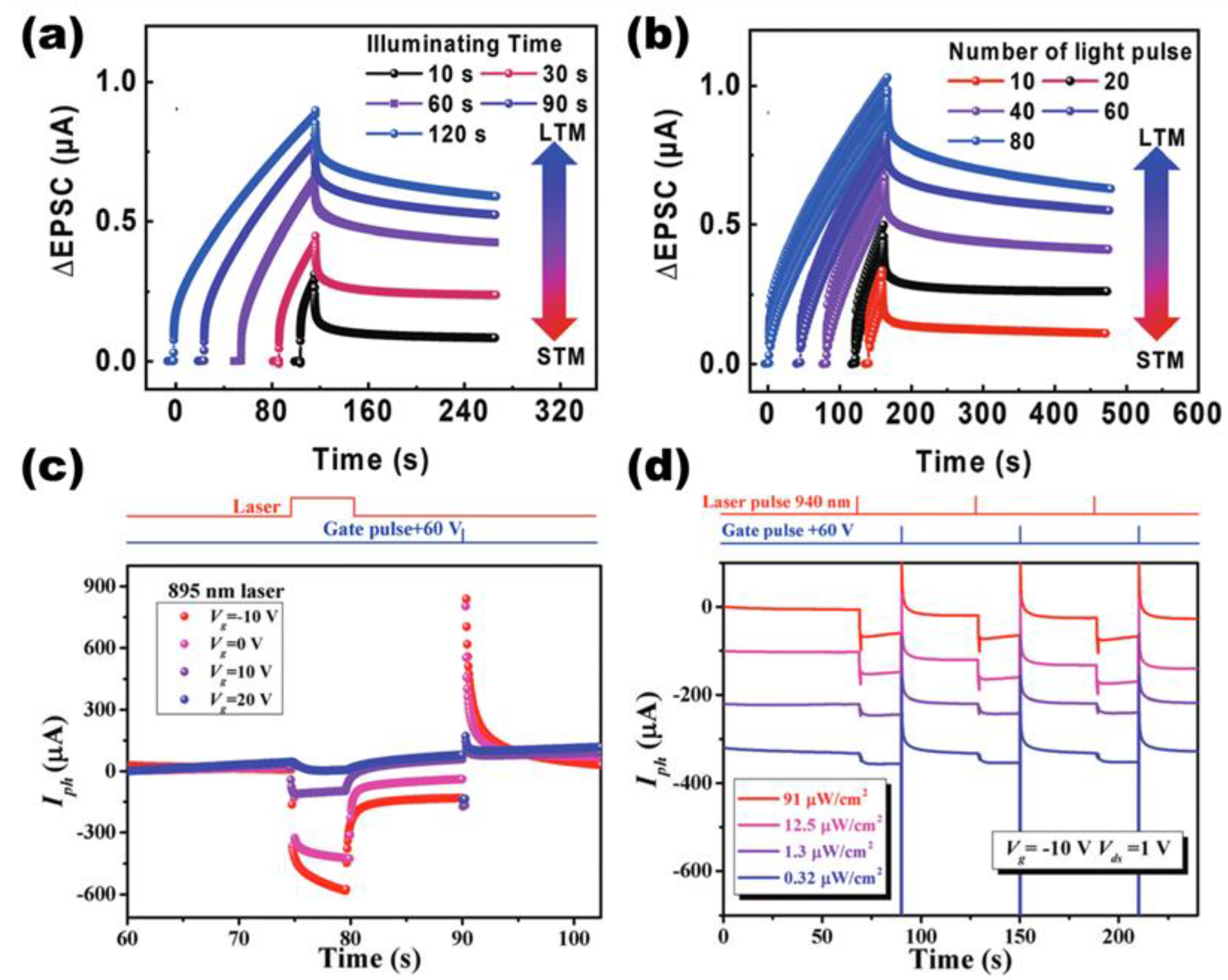
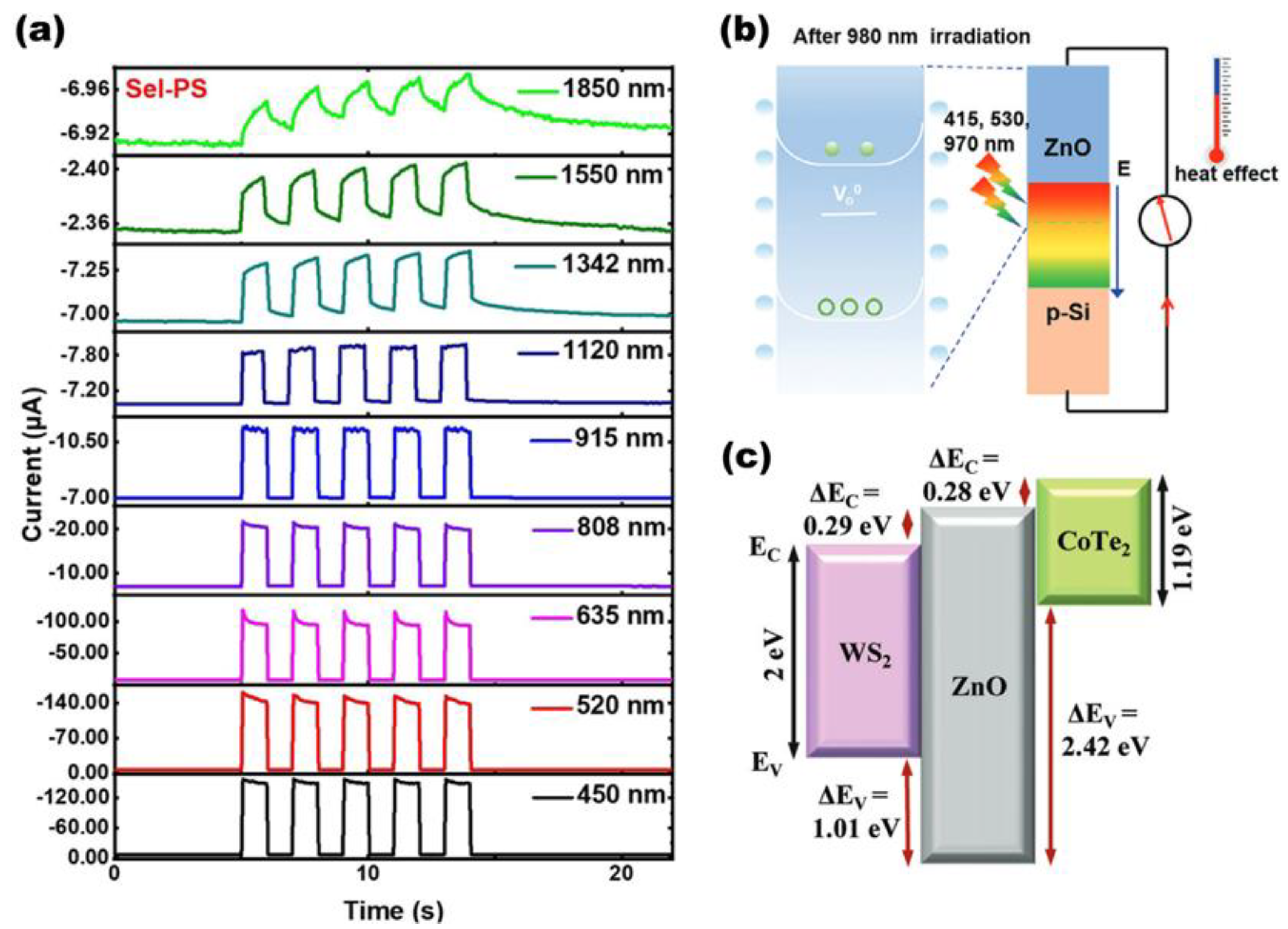
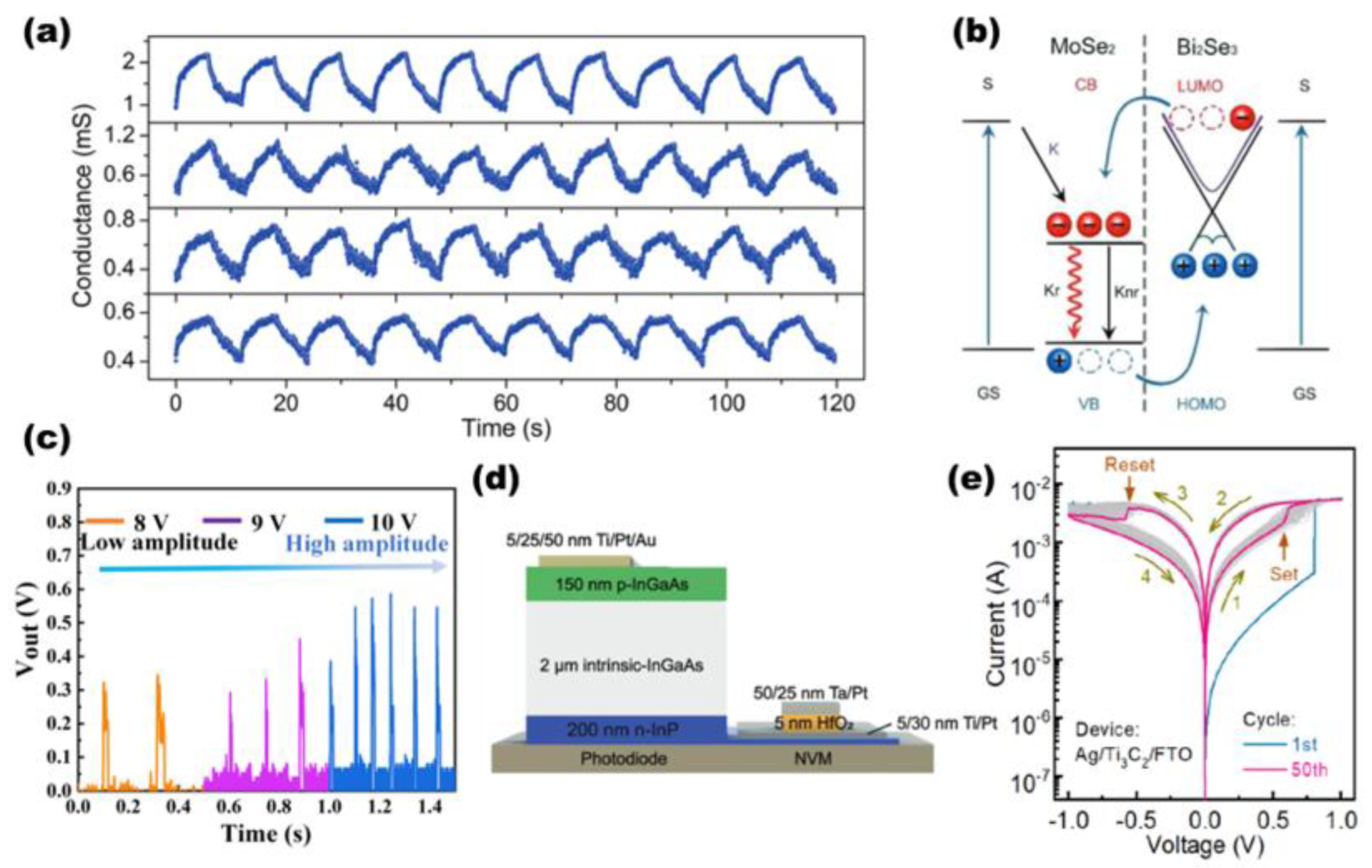
3.2. Optoelectronic Memristor for Storage and Computation

3.2.1. Photon–Electron Coupled Optoelectronic Memristor

The fundamental structure of photon–electron coupled optoelectronic memristors includes two or more electrodes and a photosensitive active material layer. When the device is illuminated, the energy of photons excites electrons in the active material, generating electron–hole pairs. The migration of these carriers alters the material’s conductivity, thus affecting the resistance state of the memristor. In some oxide semiconductor-based photonic electronic memristors, light exposure can cause the ionization and deionization of oxygen vacancies, a process similar to long-term potentiation (LTP) and long-term depression (LTD) in biological neural synapses, offering possibilities for simulating complex neural network behaviors [44]. Besides ionization and deionization processes, defect traps in photonic electronic memristors can capture and release photogenerated carriers, a mechanism crucial for realizing short-term and LTP. Furthermore, by constructing heterojunctions, such as p-n junctions or type-II heterojunctions, potential wells can be formed at interfaces, effectively limiting the recombination of photogenerated carriers, thus maintaining a longer-lasting change in conductivity following light stimulation, further emulating the dynamic behavior of neural synapses.
In 2018, Wang et al. [87] introduced a groundbreaking non-volatile infrared memory device by employing a MoS2/PbS van der Waals heterostructure. Their innovation lies in using infrared light pulses to excite holes in the PbS layer, which are then localized and modulate the MoS2’s conductivity through electrostatic interactions. Once the infrared pulse ceases, these localized holes induce electrons in the MoS2, resulting in a grating-like effect that persists without external voltage, thus retaining information post power-off. This mechanism can be further manipulated by applying gate voltage pulses, which enhance electron tunneling from MoS2 to PbS, effectively erasing the stored data. Such a cooperative control between photonic and electronic components showcases the device’s non-volatility, reconfigurability, and long-term stability. Figure 11a provides insight into the transfer characteristics of this heterostructure under varying light power densities, highlighting the dynamic changes in carrier density due to light and gate voltage injections.
Zhai et al. [88] in 2018 advanced the field by developing an infrared-sensitive memory device that employs a MoS2-upconversion nanoparticle (UCNP) heterostructure. This approach diverges from previous work that depended on direct MoS2-PbS interactions, opting instead for a controlled pyrolysis method to synthesize MoS2-UCNP nanocomposites. These nanocomposites act as NIR sensitizers and exciton generation/separation centers, significantly enhancing photogenerated carrier generation and NIR-controlled resistive switching performance. Notably, the device’s response to NIR light intensities, especially at 980 nm, is pronounced, aligning UCNPs’ emission with MoS2 nanosheets’ absorption band for efficient exciton separation. This leads to a substantial decrease in SET voltage from 4.6 V to 1.9 V under NIR illumination and an impressive increase in the on/off current ratio from 10 to 120, underscoring the device’s enhanced capabilities in infrared spectrum perception, computation, and storage. Figure 11b illustrates the energy band diagram during the SET process under 980 nm NIR illumination, showing how the photogenerated excitons and the subsequent charge separation at the interface between MoS2 and UCNPs lead to a change in the device’s resistance state.
Lai et al. [89] in 2022 further advanced the field with a non-volatile optoelectronic memory based on a MoS2/2D-RPP van der Waals heterostructure. The innovation lies in leveraging the high dielectric constant and rich interfacial states of 2D-RPP to facilitate the transition from n-type to p-type in MoS2, enabling efficient electron trapping. This design improves the device’s photoresponse and extends its operational wavelength range to include the communication band (up to 1550 nm). Figure 11c illustrates the shift in the Fermi level of MoS2 on different substrates, highlighting the p-doping effect of 2D-RPP on MoS2.
Continuing the progression, Li et al. [35] in 2023 designed a reconfigurable non-volatile neuromorphic photovoltaic detector based on MoS2. Figure 10d shows the structure of the MSM device. By plasma treating MoS2-x and introducing sulfur vacancies in the metal/MoS2-x junction, they achieved a tunable polarity change in the photogenerated current. Experiments showed that under 520 nm illumination, a 15 V/10 s pulse programming resulted in a short-circuit photocurrent change from +10 nA to −13 nA and an open-circuit voltage shift from −6 mV to +8 mV, demonstrating non-volatility. This innovation breaks the potential symmetry in MSM devices by controlling sulfur vacancy concentration, modulating the Schottky barrier height, and causing a change in the sign of the short-circuit photocurrent, which is crucial for hardware capable of detecting objects within the visible to infrared range.
In 2024, Wang et al. [90] reported on a novel tellurene (Te) material for achieving large-scale infrared bulk photovoltaic effect (BPVE) for broadband neural modulation. The BPVE response of tellurene spans a wide range from ultraviolet (390 nm) to mid-infrared (3.8 μm), with a photocurrent density as high as 70.4 A/cm2 under infrared light simulation conditions, surpassing previous semiconductors and semimetals. These enhancements signify the potential of tellurene in the development of sensing, computation, and storage devices within the infrared spectrum, paving the way for further advancements in narrow-bandgap materials for infrared BPVE applications.
Hu et al. [91] shifted the focus to all-optical control with the introduction of a synaptic memristor based on InGaZnO (IGZO) material. This device leverages light-induced electron trapping and detrapping mechanisms, allowing for continuous tuning of the memconductance by altering the wavelength of the control light. As depicted in Figure 12a, the memconductance can be reversibly modulated by 100 blue and 100 near-infrared light pulses. The device’s excellent non-volatility and the ability to perform all-optical write and erase operations in both visible and near-infrared regions open new avenues for combined photonic and electronic neuromorphic computing.
Similar to Hu et al.’s work, Li et al. [92] also focused on all-optical modulation in artificial synapses, presenting a P-MoSe2/PxOy heterostructure-based device. Using a simple one-step selenization process, they achieved modulation operations across a wide range of wavelengths (470 nm to 808 nm). Under 808 nm near-infrared light, the device can switch between short-term memory (STM) and long-term memory (LTM) modes by adjusting the light intensity, with the reset voltage varying from 0.21 V to 0.97 V under different intensities. As shown in Figure 12b, the photocurrent increases from 11.90 μA to 46.24 μA as the light intensity rises from 6 mW/cm2 to 14 mW/cm2. Continuous 808 nm light pulses (1 to 30 s) trigger the transition from STM to LTM within 2.47 to 4.27 s. These advancements are pivotal for the development of infrared-band optoelectronic devices, enabling efficient information processing without physical contact and holding promise for applications in infrared sensing and imaging.
In line with Hu et al.’s exploration of materials for all-optical control, Dong et al. [93] proposed a unique optoelectronic memristor structure comprising p-type Cu2ZnSnS4 (CZTS) nanosheets embedded in a PMMA film with Bi-OBr (BOB). This CZTS@BOB-PMMA configuration exhibits bipolar resistive switching and synaptic plasticity induced by electric fields and near-infrared light. The intimate contact and barrier-free charge transfer between CZTS and BOB, coupled with the role of oxygen vacancies in the PMMA layer as electron trapping/release centers, allow for precise control over the device’s resistance state. Under near-infrared illumination, the device displays significant photoresponsiveness, capable of mimicking various biological synaptic functions. The Nyquist plot in Figure 12c reveals the low charge transfer resistance of the CZTS@BOB nanocomposite, which facilitates the formation and disruption of conductive filaments, enabling the memristive behavior of the device.
Building on the foundation laid by Hu et al. in the realm of all-optical control, Chen et al. [34] introduced a novel device that integrates lead sulfide quantum dots (PbS QDs) with polymethyl methacrylate (PMMA), expanding the scope to broadband optoelectronics. By meticulously tuning the PMMA concentration, they optimized the device’s conductivity and photoresponse. Figure 12d demonstrates the resistance switching behavior. The device transitions from a high-resistance state to a low-resistance state as silver ions migrate and accumulate under applied voltage to form conductive filaments. Illumination of PbS QDs generates electron–hole pairs, enhancing the photoelectric response and achieving broadband light sensitivity from ultraviolet to near-infrared. With a retention capability of up to 4104 s, an on/off current ratio of 104, and a fast response time of 170 nanoseconds, the device demonstrates its versatility and efficiency in optical applications.
Similarly, Zhu et al. [94] developed an optoelectronic artificial synapse based on amorphous silicon–tin alloy (a-Si1−xSnx) films. This device achieves broadband response from visible to near-infrared-I wavelengths through oxygen vacancy band engineering and heterostructure design. Notably, it demonstrates ultra-long decay times (3576.07 s) and broadband response, significantly enhancing the photoresponse characteristics of the device in the visible to near-infrared region. By adjusting the read voltage to simulate “pupil” dilation effects on image memory, the device’s potential in simulating human visual memory is highlighted.

3.2.2. Conductive Filament Memristor

The core operating principle of conductive filament-type memristors involves the formation of conductive filaments between electrodes to store data. This type of memristor consists of two electrodes and an intervening storage medium layer, typically composed of electrochemically active materials such as metal oxides or sulfides. In an unprogrammed state, the memristor exhibits a high resistance state representing a “0”; whereas in a programmed state, by applying a high voltage to induce ion migration within the material and form a conductive path, known as a conductive filament, between the electrodes, the resistance decreases, representing a “1”.
The formation of conductive filaments is analogous to electrochemical metallization; when a sufficiently high voltage is applied, the electric field drives the migration of ions, which accumulate between the electrodes to form a conductive pathway. This process can be precisely controlled by altering the voltage and current, thereby regulating the resistance state of the memristor and enabling multi-level storage [95]. To erase stored data, i.e., return to an HRS, a lower voltage or brief current pulse can be applied, causing the conductive filament to break. The breaking of the conductive filament may be due to the reflow of ions or structural changes in the material induced by the electric field, resulting in the discontinuity of the conductive filament.
The non-volatile characteristic of conductive filament-type memristors means that they retain their resistance state even after power is removed, which is critical for data retention. Additionally, this type of memristor structure is simple, consumes low power, operates at high speeds, and has good scalability, making it an ideal choice for applications such as neuromorphic computing systems [15,49].
In 2016, Wang et al. [96] introduced a SiO2 ion diffusion limiting layer (DLL) into TaOx-based memristors, marking a significant advancement in controlling the growth and dissolution of conductive filaments. By limiting the number of oxygen ions/vacancies involved in the initial stages, the SiO2 layer homogenizes the growth/dissolution rate, reducing non-linear behavior and enabling more uniform and linear conductivity changes under the same electrical pulse stimulation. Figure 13a illustrates the repetitive potentiation/depression cycles of TaOx-based memristors with different thicknesses of the SiO2 DLL. The figure shows ten repetitive P/D cycles of memristors without the SiO2 layer, and with 1 nm, 2 nm, and 4 nm SiO2 layers, each cycle consisting of 300 identical pulses. These data highlight a substantial improvement in the linearity of conductance modulation, crucial for synaptic weight adjustment in brain-like computing hardware. Additionally, the SiO2 layer reduces device power consumption, allowing researchers to implement important synaptic learning rules, such as Spike-Timing-Dependent Plasticity (STDP).
Building on the concept of controlling conductive filament growth, Wang et al. [97] in 2019 introduced an NIR-controllable memristor based on quasi-two-dimensional MoSe2/Bi2Se3 heterostructures. This design leverages the effective separation of electron–hole pairs under NIR illumination, where electrons are captured by MoSe2, forming an internal electric field that promotes hole transport through the heterostructure. Active holes colliding with Ag conductive filaments oxidize Ag clusters back to Ag+ cations, dissolving and breaking the conductive path, switching the device from the LRS to HRS state. Figure 13b illustrates the dynamic behavior of photogenerated charge carriers in the MoSe2/Bi2Se3 heterostructure under different operational states. The memristor demonstrated an on/off ratio of about 104 in dark conditions and achieved threshold switching and reset operations under NIR illumination, significantly enhancing response and detection sensitivity. This NIR-modulated effect not only allows for non-volatile control of conductive filaments but also mimics the transmission functions of biological synapses.
In 2023, Yan et al. [98] took the next step by proposing artificial sensory neurons based on NdNiO3 (NNO) nanocrystalline thin films. The unique metallic phase nanocrystals enhance the local electric field and act as a reservoir for defects (VoS), guiding the growth of conductive filaments and stabilizing device performance. They demonstrated stable bidirectional threshold switching behavior with a set power as low as 120 nW and showed a reduction in operation voltage due to the effect of photogenerated carriers under light conditions. The device achieved basic functionalities of leaky integrate-and-fire (LIF) neurons, including all-or-nothing spikes, threshold-driven firing, refractory periods, and spike frequency modulation. Figure 13c shows the response of the artificial neuron circuit under different pulse amplitudes, indicating that spike frequency increases with increasing pulse amplitude due to faster overall charging speed. This demonstrates that the artificial neuron successfully achieves intensity-modulated spike frequency characteristics similar to those of biological neurons, making it suitable for simulating scenarios such as ships approaching a harbor at night. Experimental results indicate that NNO-based artificial sensory neurons provide a viable route for constructing efficient sensory systems using micro-devices.
Expanding the application to imaging, Bae et al. [99] demonstrated a pixel array constructed by heterogeneously integrating an InGaAs photodiode with a non-volatile HfO2-based memristor (NVM) for NIR image processing. As shown in Figure 13d, the design employs a one photodiode and one resistor (1P-1R) structure, where the InGaAs p-i-n photodiode consists of 150 nm of p-type InGaAs, 2 μm of intrinsic InGaAs, and 200 nm of n-type InP. The external quantum efficiency (EQE) of this photodiode reached 55%, with a responsivity of 34.59 A/W and a detectivity of 2.54 × 1012 cm·Hz1/2/W, achieving a response time of 60.0 ns. These enhanced performance metrics enable the device to achieve efficient optical sensing, computation, and storage within the NIR band. The HfO2-based NVM exhibited excellent linear conductance modulation capabilities, suitable for linear regression tasks in gradient algorithms. Moreover, the NVM displayed excellent retention post-set, with only a 0.1% change. This study not only provides a new design concept for NIR sensors but also demonstrates the possibility of implementing complex computations on-chip, advancing the development of NIR ISC devices.
Yue et al. [100] proposed a novel optoelectronic memristor using Ti3C2 MXene material, showcasing non-volatile storage characteristics and achieving multiple synaptic behaviors via electro-optical synergistic control, including STDP, PPF, LTP/LTD, etc. Ti3C2 MXene serves as the active layer of the memristor, with its large interlayer spacing and rich surface functional groups providing favorable conditions for tuning the device’s conductivity. Figure 13e illustrates the typical cyclic I-V characteristics of the Ti3C2 MXene-based memristor, indicating the device’s excellent non-volatile bipolar resistive switching behavior, fundamental to understanding its storage and synaptic functions. The selection of materials and structural design enable the device to exhibit outstanding response capability in the near-infrared wavelength range, providing a new direction for the development of ISC devices.

4. Infrared Neural Network

Building on the research of infrared artificial synapses based on two-terminal memristors and three-terminal transistors, researchers have further integrated sensing, storage, and information processing functions using optoelectronic neuromorphic devices to emulate biological visual systems [6,26,46]. Corresponding to the visible light visual system’s perception and recognition of colors through wavelength information, infrared light visual systems can be developed to recognize temperature information. This can serve as a basis for distinguishing objects. Gesture recognition, a key technology in the field of human–computer interaction, has been extensively researched and applied in recent years. By combining infrared detection signals with motion detection devices or image recognition systems, efficient detection of object motion information can be achieved.
Wang et al. [101] proposed an infrared near-sensor reservoir computing (RC) system, integrating infrared sensors and memristors based on single-crystalline LiTaO3 (LT) and LiNbO3 (LN) thin films, respectively. The system is designed to process sensor signals with spatiotemporal characteristics efficiently. As shown in Figure 14a, the infrared sensor array consists of 16 × 1 LT-based pyroelectric infrared sensors, which convert the infrared signals into analog voltage signals. The memristor array comprises 16 LN-based memristors, each with a structure of Au/LN/Cr/Pt/Cr. The memristors are used as the reservoir in the RC system to process the sensor signals. The software readout layer is a 16 × 9 single-layer perceptron (SLP). The infrared near-sensor RC system is used for dynamic gesture perception. As shown in Figure 14b, the system records sensor signals of three classes of moving gestures (“Scissor”, “Rock”, and “Paper”) at a sampling frequency of 3.33 Hz. The gestures move parallel to the axis of the sensing window at a speed of 0.75 cm/s and are completed in 20 time steps. The system achieves a recognition accuracy of 100% for gestures at a detection distance of 4 cm and an average accuracy of 99.6% for gestures at different detection distances (3.5 cm, 4 cm, 4.5 cm). Liang et al. [102] developed an infrared (IR) gesture recognition system using a near-sensor computing architecture. The system integrates a 3 × 3 IR thermopile sensor array fabricated with MEMS technology and an artificial neural network (ANN). The thermopile sensors feature a SiO2 supporting layer on a silicon substrate, with a cavity for thermal isolation. Thermocouples, made of p-type polysilicon and aluminum, are arranged symmetrically to optimize output voltage. The absorber layer, composed of Si3N4, absorbs IR radiation and converts it to heat. Graphene oxide (GO) was transferred to the absorber layers using a non-destructive method, increasing IR absorption by 61.1% and responsivity to 705.1 V/W, an 85.9% improvement. The gesture recognition system uses a near-sensor computing architecture, including the IR thermopile sensor array, a microcontroller unit (MCU), a local server, and MicroPython firmware. The ANN model, designed in TensorFlow-Lite (TF-Lite), consists of an input layer with nine neurons, a hidden layer with six neurons, and an output layer with three neurons. Activation functions are logsig and ReLU, and the loss function is mean square error. Training uses the gradient descent method. The trained model is deployed on edge devices for inference, reducing latency and power consumption. Tests on “rock”, “paper”, and “scissors” gestures showed that GO improved response voltages and recognition sensitivity. The system with GO-enhanced sensors achieved 100% recognition accuracy.
Furthermore, by mimicking the memory function of neurons with memristors, artificial vision systems can achieve long-term or short-term memory of detected images. Such infrared perception systems fill the gap in nighttime image acquisition and memory functions, allowing the characteristic information of objects at night to be well remembered and processed. Chen et al. [103] developed a self-powered flexible artificial synapse for near-infrared (NIR) light detection, integrating light sensing, processing, and memory functions. The flexible array sensor consists of a patterned array on a PET substrate, where the electrodes are prepared by photolithography and a polymethyl methacrylate (PMMA) layer is spin-coated on top of the polymer PBTT as an encapsulation layer. This design allows the device to recognize and memorize input Chinese character images composed of 9 × 11 pixels. As shown in Figure 14c, Upon the first light stimulus at 915 nm (100 mW/cm2, 1 Hz), the characters begin to emerge, with the photocurrent increasing to approximately 5 pA. As the number of pulse stimulations increases, the characters become more distinct, and the circuit current gradually improves, reaching 11 pA after five stimulations. After the irradiation ceases, the character images fade slowly, with the current decreasing to 8 pA after 2 s. This behavior demonstrates the device’s ability to perceive and record external NIR light, mimicking the human visual system’s ability to retain and fade visual information over time. The visual memory system’s performance is further characterized by its ability to maintain the recorded information over extended periods. The flexible devices exhibit excellent mechanical and electrical stability, retaining their photoresponse and synaptic behaviors even after 1000 bending cycles and remaining stable for at least one month under ambient conditions. These properties make the flexible self-powered optical synapses highly suitable for applications in wearable devices and bionic retinas, where long-term stability and reliability are crucial.

5. Conclusions and Perspectives

In summary, researchers are advancing the development of ISC devices along the lines of multi-band response, material innovation, neuromorphic computing, and integration compatibility. These studies not only broaden the application scope of devices but also improve their performance, making them more suited to practical needs. Table 1 summarizes the high-performance infrared ISC devices mentioned in this article, highlighting the progress made in this field.
Overall, researchers are advancing the development of optoelectronic synaptic devices along the paths of multi-band response, material innovation, neuromorphic computing, and integration and compatibility. An increasing number of these devices are being designed to respond to light signals from ultraviolet to near-infrared and even mid-infrared bands. This enhancement in multi-band response capability indicates that researchers are striving to expand the applicability of these devices to meet a broader range of real-world application demands. Moreover, researchers are continuously exploring new material systems. Two-dimensional materials such as MoS2, In2Se3, and black phosphorus have become hotspots in research due to their unique physical properties. These materials significantly enhance photoelectric conversion efficiency while exhibiting excellent mechanical flexibility and compatibility with other materials. To achieve miniaturization and integration of devices, researchers consider compatibility with existing manufacturing processes during the design phase. For instance, combining two-dimensional materials with traditional semiconductor materials extends the application range of devices and simultaneously enhances their performance, rendering them better suited for practical application requirements.
However, there are still some limitations in current research. For instance, many classic neuromorphic device structures that perform well in the visible light band have yet to be applied to the infrared band, such as photon–ion coupled, phase-change, ferroelectric memristors or transistors [15,36]. Researchers can attempt to utilize light signals to control the migration of ions, the transition between different phases (such as crystalline and amorphous states) of materials, or the polarization state of ferroelectric materials [110] to construct optoelectronic synaptic devices with infrared response. If these working mechanisms could be introduced into infrared band devices and their performance optimized, it might bring about new technological breakthroughs.
Furthermore, existing research predominantly focuses on wide-spectrum responsive devices, with insufficient exploration of specific bands such as MWIR. Materials like tellurene (Te) exhibit high photocurrent density across a broad spectral range, but materials with good infrared band response, such as mercury telluride [111], require further exploration in ISC devices.
Moreover, existing research often evaluates the learning or computational performance of devices through specific application scenarios and simple neural networks. However, these test scenarios rarely consider the actual application needs of infrared detection, such as night vision, remote sensing monitoring, medical diagnosis, and industrial inspection. Only a few studies have provided simulations tailored to infrared band applications, such as nighttime vessel docking [98], gesture recognition [102], or vein detection [99], etc. Therefore, designing dedicated testing platforms and application scenarios that conform to the characteristics of infrared detection will be necessary in future research. This will help better evaluate the actual performance and applicability of ISC devices in infrared detection, thereby promoting their practical application.
Overall, although significant progress has been made in multi-band response, material innovation, neuromorphic computing, and integration compatibility, the aforementioned limitations must be overcome to realize the widespread application of infrared band ISC devices. By incorporating the working mechanisms of classic neuromorphic devices, delving deeper into new materials suitable for the MWIR band, and designing application scenarios that meet actual needs, it is hoped that further advancement in this field will lead to significant breakthroughs in the application of ISC devices in the infrared detection domain.

Author Contributions

Conceptualization, T.Q. and W.F.; investigation, T.Q. and W.F.; data curation, W.F.; writing—original draft preparation, W.F.; writing—review and editing, T.Q. and X.T.; supervision, T.Q.; funding acquisition, T.Q. and X.T. All authors have read and agreed to the published version of the manuscript.

Funding

This research was funded by the National Key R&D Program of China (2021YFA0717600), the National Natural Science Foundation of China (NSFC No. 62035004, NSFC No. U22A2081), the Young Elite Scientists Sponsorship Program by CAST (No. YESS20200163), and the BIT Research and Innovation Promoting Project (grant no. 2024YCXZ019).

Institutional Review Board Statement

Not applicable.

Informed Consent Statement

Not applicable.

Data Availability Statement

Not applicable.

Conflicts of Interest

The authors declare no conflicts of interest.

References

  1. Zhou, F.; Chai, Y. Near-Sensor and in-Sensor Computing. Nat. Electron. 2020, 3, 664–671. [Google Scholar] [CrossRef]
  2. Ielmini, D.; Wong, H.-S.P. In-Memory Computing with Resistive Switching Devices. Nat. Electron. 2018, 1, 333–343. [Google Scholar] [CrossRef]
  3. Strukov, D.B.; Snider, G.S.; Stewart, D.R.; Williams, R.S. The Missing Memristor Found. Nature 2008, 453, 80–83. [Google Scholar] [CrossRef] [PubMed]
  4. Zhang, K.; Meng, D.; Bai, F.; Zhai, J.; Wang, Z.L. Photon-Memristive System for Logic Calculation and Nonvolatile Photonic Storage. Adv. Funct. Mater. 2020, 30, 2002945. [Google Scholar] [CrossRef]
  5. Dai, S.; Zhao, Y.; Wang, Y.; Zhang, J.; Fang, L.; Jin, S.; Shao, Y.; Huang, J. Recent Advances in Transistor-Based Artificial Synapses. Adv. Funct. Mater. 2019, 29, 1903700. [Google Scholar] [CrossRef]
  6. Sun, B.; Guo, T.; Zhou, G.; Ranjan, S.; Jiao, Y.; Wei, L.; Zhou, Y.N.; Wu, A.Y. Synaptic Devices Based Neuromorphic Computing Applications in Artificial Intelligence. Mater. Today Phys. 2021, 18, 100393. [Google Scholar] [CrossRef]
  7. Liu, Y.; Fan, R.; Guo, J.; Ni, H.; Bhutta, M.U.M. In-Sensor Visual Perception and Inference. Intell. Comput. 2023, 2, 0043. [Google Scholar] [CrossRef]
  8. Yang, Y.; Pan, C.; Li, Y.; Yangdong, X.; Wang, P.; Li, Z.-A.; Wang, S.; Yu, W.; Liu, G.; Cheng, B.; et al. In-Sensor Dynamic Computing for Intelligent Machine Vision. Nat. Electron. 2024, 7, 225–233. [Google Scholar] [CrossRef]
  9. Zhao, H.; Liu, Z.; Tang, J.; Gao, B.; Zhang, Y.; Qian, H.; Wu, H. Memristor-Based Signal Processing for Edge Computing. Tsinghua Sci. Technol. 2022, 27, 455–471. [Google Scholar] [CrossRef]
  10. Park, H.-L.; Lee, Y.; Kim, N.; Seo, D.-G.; Go, G.-T.; Lee, T.-W. Flexible Neuromorphic Electronics for Computing, Soft Robotics, and Neuroprosthetics. Adv. Mater. 2020, 32, 1903558. [Google Scholar] [CrossRef]
  11. Wang, B.; Zhang, Y.; You, J.; Yang, M.; Han, Z.; Lin, D.; Liu, M.; Zhang, N.; Jiang, Z.; Guo, H.; et al. An Image Detection–Memory–Recognition Artificial Visual Unit Based on Dual-Gate Phototransistors. Adv. Intell. Syst. 2023, 5, 2200328. [Google Scholar] [CrossRef]
  12. Liu, S.; Liu, L.; Tang, J.; Yu, B.; Wang, Y.; Shi, W. Edge Computing for Autonomous Driving: Opportunities and Challenges. Proc. IEEE 2019, 107, 1697–1716. [Google Scholar] [CrossRef]
  13. He, Y.; Deng, B.; Wang, H.; Cheng, L.; Zhou, K.; Cai, S.; Ciampa, F. Infrared Machine Vision and Infrared Thermography with Deep Learning: A Review. Infrared Phys. Technol. 2021, 116, 103754. [Google Scholar] [CrossRef]
  14. Tan, C.L.; Mohseni, H. Emerging Technologies for High Performance Infrared Detectors. Nanophotonics 2018, 7, 169–197. [Google Scholar] [CrossRef]
  15. Wang, J.; Ilyas, N.; Ren, Y.; Ji, Y.; Li, S.; Li, C.; Liu, F.; Gu, D.; Ang, K.-W. Technology and Integration Roadmap for Optoelectronic Memristor. Adv. Mater. 2024, 36, e2307393. [Google Scholar] [CrossRef]
  16. Hu, L.; Zhuge, X.; Wang, J.; Wei, X.; Zhang, L.; Chai, Y.; Xue, X.; Ye, Z.; Zhuge, F. Emerging Optoelectronic Devices for Brain-Inspired Computing. Adv. Elect. Mater. 2024, 2400482. [Google Scholar] [CrossRef]
  17. Rogalski, A. Scaling Infrared Detectors—Status and Outlook. Rep. Prog. Phys. 2022, 85, 126501. [Google Scholar] [CrossRef]
  18. Zeng, L.; Wu, D.; Jie, J.; Ren, X.; Hu, X.; Lau, S.P.; Chai, Y.; Tsang, Y.H. Van Der Waals Epitaxial Growth of Mosaic-Like 2D Platinum Ditelluride Layers for Room-Temperature Mid-Infrared Photodetection up to 10.6 Μm. Adv. Mater. 2020, 32, 2004412. [Google Scholar] [CrossRef] [PubMed]
  19. Zeng, L.; Han, W.; Ren, X.; Li, X.; Wu, D.; Liu, S.; Wang, H.; Lau, S.P.; Tsang, Y.H.; Shan, C.-X.; et al. Uncooled Mid-Infrared Sensing Enabled by Chip-Integrated Low-Temperature-Grown 2D PdTe2 Dirac Semimetal. Nano Lett. 2023, 23, 8241–8248. [Google Scholar] [CrossRef] [PubMed]
  20. Rogalski, A.; Kopytko, M.; Hu, W.; Martyniuk, P. Infrared HOT Photodetectors: Status and Outlook. Sensors 2023, 23, 7564. [Google Scholar] [CrossRef]
  21. Wang, H.; Li, Z.; Li, D.; Chen, P.; Pi, L.; Zhou, X.; Zhai, T. Van Der Waals Integration Based on Two-Dimensional Materials for High-Performance Infrared Photodetectors. Adv. Funct. Mater. 2021, 31, 2103106. [Google Scholar] [CrossRef]
  22. Wang, C.; Zhang, X.; Hu, W. Organic Photodiodes and Phototransistors toward Infrared Detection: Materials, Devices, and Applications. Chem. Soc. Rev. 2020, 49, 653–670. [Google Scholar] [CrossRef]
  23. Tian, Y.; Luo, H.; Chen, M.; Li, C.; Kershaw, S.V.; Zhang, R.; Rogach, A.L. Mercury Chalcogenide Colloidal Quantum Dots for Infrared Photodetection: From Synthesis to Device Applications. Nanoscale 2023, 15, 6476–6504. [Google Scholar] [CrossRef]
  24. Wu, D.; Guo, C.; Zeng, L.; Ren, X.; Shi, Z.; Wen, L.; Chen, Q.; Zhang, M.; Li, X.J.; Shan, C.-X.; et al. Phase-Controlled van Der Waals Growth of Wafer-Scale 2D MoTe2 Layers for Integrated High-Sensitivity Broadband Infrared Photodetection. Light. Sci. Appl. 2023, 12, 5. [Google Scholar] [CrossRef] [PubMed]
  25. Wu, D.; Mo, Z.; Li, X.; Ren, X.; Shi, Z.; Li, X.; Zhang, L.; Yu, X.; Peng, H.; Zeng, L.; et al. Integrated Mid-Infrared Sensing and Ultrashort Lasers Based on Wafer-Level Td-WTe2 Weyl Semimetal. Appl. Phys. Rev. 2024, 11, 041401. [Google Scholar] [CrossRef]
  26. Huang, Y.; Tan, Y.; Kang, Y.; Chen, Y.; Tang, Y.; Jiang, T. Bioinspired Sensing-Memory-Computing Integrated Vision Systems: Biomimetic Mechanisms, Design Principles, and Applications. Sci. China Inf. Sci. 2024, 67, 151401. [Google Scholar] [CrossRef]
  27. Zhang, M.; Xu, Z.; Chen, J.; Ju, Z.; Ma, Y.; Niu, Z.; Xu, Z.; Zhang, T.; Shi, F. Recent Advances on Nanomaterials-Based Photothermal Sensing Systems. Trac-Trends Anal. Chem. 2024, 177, 117801. [Google Scholar] [CrossRef]
  28. Zhu, X.; Cai, Z.; Wu, Q.; Wu, J.; Liu, S.; Chen, X.; Zhao, Q. 2D Black Phosphorus Infrared Photodetectors. Laser Photonics Rev. 2024, 12, 2400703. [Google Scholar] [CrossRef]
  29. Zhang, J.; Guo, P.; Guo, Z.; Li, L.; Sun, T.; Liu, D.; Li, T.; Zu, G.; Xiong, L.; Zhang, J.; et al. Retina-Inspired Artificial Synapses with Ultraviolet to Near-Infrared Broadband Responses for Energy-Efficient Neuromorphic Visual Systems. Adv. Funct. Mater. 2023, 33, 2302885. [Google Scholar] [CrossRef]
  30. Das, S.; Pal, V.; Mukherjee, S.; Das, S.; Tiwary, C.S.; Ray, S.K. Multi-Wavelength Optoelectronic Synaptic Transistors Based on Transition Metal Telluride-Sulfide Heterostructures. Adv. Opt. Mater. 2024, 12, 2400037. [Google Scholar] [CrossRef]
  31. Guo, F.; Liu, Y.; Zhang, M.; Yu, W.; Li, S.; Zhang, B.; Hu, B.; Li, S.; Sun, A.; Jiang, J.; et al. VO2 /MoO3 Heterojunctions Artificial Optoelectronic Synapse Devices for Near-Infrared Optical Communication. Small 2024, 20, e2310767. [Google Scholar] [CrossRef]
  32. Ercan, E.; Lin, Y.; Sakai-Otsuka, Y.; Borsali, R.; Chen, W. Harnessing Biobased Materials in Photosynaptic Transistors with Multibit Data Storage and Panchromatic Photoresponses Extended to Near-Infrared Band. Adv. Opt. Mater. 2022, 10, 2201240. [Google Scholar] [CrossRef]
  33. Zhu, Y.; Wang, Y.; Pang, X.; Jiang, Y.; Liu, X.; Li, Q.; Wang, Z.; Liu, C.; Hu, W.; Zhou, P. Non-Volatile 2D MoS2/Black Phosphorus Heterojunction Photodiodes in the near- to Mid-Infrared Region. Nat. Commun. 2024, 15, 6015. [Google Scholar] [CrossRef]
  34. Chen, Z.; Yu, Y.; Jin, L.; Li, Y.; Li, Q.; Li, T.; Lucas, P.W.; Li, J.; Zhao, H.; Zhang, Y.; et al. Broadband Photoelectric Tunable Quantum Dot Based Resistive Random Access Memory. J. Mater. Chem. C 2020, 8, 2178–2185. [Google Scholar] [CrossRef]
  35. Li, T.; Miao, J.; Fu, X.; Song, B.; Cai, B.; Ge, X.; Zhou, X.; Zhou, P.; Wang, X.; Jariwala, D.; et al. Reconfigurable, Non-Volatile Neuromorphic Photovoltaics. Nat. Nanotechnol. 2023, 18, 1303–1310. [Google Scholar] [CrossRef]
  36. Zhu, J.; Zhang, T.; Yang, Y.; Huang, R. A Comprehensive Review on Emerging Artificial Neuromorphic Devices. Appl. Phys. Rev. 2020, 7, 011312. [Google Scholar] [CrossRef]
  37. Tang, J.; Yuan, F.; Shen, X.; Wang, Z.; Rao, M.; He, Y.; Sun, Y.; Li, X.; Zhang, W.; Li, Y.; et al. Bridging Biological and Artificial Neural Networks with Emerging Neuromorphic Devices: Fundamentals, Progress, and Challenges. Adv. Mater. 2019, 31, 1902761. [Google Scholar] [CrossRef] [PubMed]
  38. Chua, L. Memristor-The Missing Circuit Element. IEEE Trans. Circuit Theory 1971, 18, 507–519. [Google Scholar] [CrossRef]
  39. Zidan, M.A.; Strachan, J.P.; Lu, W.D. The Future of Electronics Based on Memristive Systems. Nat. Electron. 2018, 1, 22–29. [Google Scholar] [CrossRef]
  40. Wang, Z.; Wu, H.; Burr, G.W.; Hwang, C.S.; Wang, K.L.; Xia, Q.; Yang, J.J. Resistive Switching Materials for Information Processing. Nat. Rev. Mater. 2020, 5, 173–195. [Google Scholar] [CrossRef]
  41. Tanim, M.M.H.; Templin, Z.; Zhao, F. Natural Organic Materials Based Memristors and Transistors for Artificial Synaptic Devices in Sustainable Neuromorphic Computing Systems. Micromachines 2023, 14, 235. [Google Scholar] [CrossRef] [PubMed]
  42. Li, Z.; Tang, W.; Zhang, B.; Yang, R.; Miao, X. Emerging Memristive Neurons for Neuromorphic Computing and Sensing. Sci. Technol. Adv. Mater. 2023, 24, 2188878. [Google Scholar] [CrossRef]
  43. Diorio, C.; Hasler, P.; Minch, A.; Mead, C.A. A Single-Transistor Silicon Synapse. IEEE Trans. Electron. Devices 1996, 43, 1972–1980. [Google Scholar] [CrossRef]
  44. Wang, Y.; Yin, L.; Huang, W.; Li, Y.; Huang, S.; Zhu, Y.; Yang, D.; Pi, X. Optoelectronic Synaptic Devices for Neuromorphic Computing. Adv. Intell. Syst. 2021, 3, 2000099. [Google Scholar] [CrossRef]
  45. Han, C.; Han, X.; Han, J.; He, M.; Peng, S.; Zhang, C.; Liu, X.; Gou, J.; Wang, J. Light-Stimulated Synaptic Transistor with High PPF Feature for Artificial Visual Perception System Application. Adv. Funct. Mater. 2022, 32, 2113053. [Google Scholar] [CrossRef]
  46. Wang, X.; Zong, Y.; Liu, D.; Yang, J.; Wei, Z. Advanced Optoelectronic Devices for Neuromorphic Analog Based on Low-Dimensional Semiconductors. Adv. Funct. Mater. 2023, 33, 2213894. [Google Scholar] [CrossRef]
  47. Dai, S.; Liu, X.; Liu, Y.; Xu, Y.; Zhang, J.; Wu, Y.; Cheng, P.; Xiong, L.; Huang, J. Emerging Iontronic Neural Devices for Neuromorphic Sensory Computing. Adv. Mater. 2023, 35, 2300329. [Google Scholar] [CrossRef]
  48. Han, J.; Yun, S.; Lee, S.; Yu, J.; Choi, Y. A Review of Artificial Spiking Neuron Devices for Neural Processing and Sensing. Adv. Funct. Mater. 2022, 32, 2204102. [Google Scholar] [CrossRef]
  49. Yu, S. Neuro-Inspired Computing With Emerging Nonvolatile Memory. Proc. IEEE 2018, 106, 260–285. [Google Scholar] [CrossRef]
  50. Hou, Y.; Li, Y.; Zhang, Z.; Li, J.; Li, J.; Qi, D.-H.; Chen, X.; Wang, J.; Yao, B.-W.; Yu, M.-X.; et al. Large-Scale and Flexible Optical Synapses for Neuromorphic Computing and Integrated Visible Information Sensing Memory Processing. ACS Nano 2020, 15, 1497–1508. [Google Scholar] [CrossRef]
  51. Roldan, R.; Silva-Guillen, J.A.; Pilar Lopez-Sancho, M.; Guinea, F.; Cappelluti, E.; Ordejon, P. Electronic Properties of Single-Layer and Multilayer Transition Metal Dichalcogenides MX2 (M = Mo, W and X = S, Se). Ann. Phys. Berl. 2014, 526, 347–357. [Google Scholar] [CrossRef]
  52. Wang, Y.; Yang, J.; Fraser, M.; Ye, W.; She, D.; Chen, J.; Lv, Z.; Roy, V.A.L.; Li, H.; Zhou, K.; et al. Near-Infrared-Irradiation-Mediated Synaptic Behavior from Tunable Charge-Trapping Dynamics. Adv. Electron. Mater. 2020, 6, 1900765. [Google Scholar] [CrossRef]
  53. Yang, H.; Hu, Y.; Zhang, X.; Ding, Y.; Wang, S.; Su, Z.; Shuai, Y.; Hu, P. Near-Infrared Optical Synapses Based on Multilayer MoSe2 Moiré Superlattice for Artificial Retina. Adv. Funct. Mater. 2023, 34, 2308149. [Google Scholar] [CrossRef]
  54. Hou, P.F.; Tan, S.; Zheng, S. Design and Implementation of an Infrared Artificial Visual Neural Synapse Based on P-WSe2/n-Ta2NiS5 van Der Waals Heterojunction. J. Mater. Chem. C 2024, 12, 16722–16731. [Google Scholar] [CrossRef]
  55. Taffelli, A.; Dire, S.; Quaranta, A.; Pancheri, L. MoS2 Based Photodetectors: A Review. Sensors 2021, 21, 2758. [Google Scholar] [CrossRef]
  56. Kim, S.G.; Kim, S.H.; Kim, G.S.; Park, J.; Park, J.H.; Kim, J.; Saraswat, K.C.; Kim, J.; Yu, H.Y. Infrared Detectable MoS2 Phototransistor and Its Application to Artificial Multilevel Optic-Neural Synapse. ACS Nano 2019, 13, 10294–10300. [Google Scholar] [CrossRef]
  57. Islam, M.M.; Krishnaprasad, A.; Dev, D.; Martinez-Martinez, R.; Okonkwo, V.; Wu, B.; Han, S.S.; Bae, T.-S.; Chung, H.-S.; Touma, J.; et al. Multiwavelength Optoelectronic Synapse with 2D Materials for Mixed-Color Pattern Recognition. ACS Nano 2022, 16, 10188–10198. [Google Scholar] [CrossRef] [PubMed]
  58. Li, Y.; Yang, Z.; Wang, Y.; Sun, J.; You, Q.; Zhu, M.; Li, L.; Deng, T. Polarization-Sensitive Optoelectronic Synapse Based on 3D Graphene/MoS2 Heterostructure. Adv. Funct. Mater. 2023, 34, 2302288. [Google Scholar] [CrossRef]
  59. Mukherjee, S.; Koren, E. Indium Selenide (In2Se3)—An Emerging Van-Der-Waals Material for Photodetection and Non-Volatile Memory Applications. Isr. J. Chem. 2022, 62, e202100112. [Google Scholar] [CrossRef]
  60. Hu, Y.; Yang, H.; Huang, J.; Zhang, X.; Tan, B.; Shang, H.; Zhang, S.; Feng, W.; Zhu, J.; Zhang, J.; et al. Flexible Optical Synapses Based on In2Se3/MoS2 Heterojunctions for Artificial Vision Systems in the Near-Infrared Range. ACS Appl. Mater. Interfaces 2022, 14, 55839–55849. [Google Scholar] [CrossRef]
  61. Li, X.; Li, S.; Tang, B.; Liao, J.; Chen, Q. A Vis-SWIR Photonic Synapse with Low Power Consumption Based on WSe 2 /In 2 Se 3 Ferroelectric Heterostructure. Adv. Elect. Mater. 2022, 8, 2200343. [Google Scholar] [CrossRef]
  62. Yan, T.; Cai, Y.; Wang, Y.; Yang, J.; Li, S.; Zhan, X.; Wang, F.; Cheng, R.; Wang, F.; He, J.; et al. Near-Infrared Optoelectronic Synapses Based on a Te/α-In2Se3 Heterojunction for Neuromorphic Computing. Sci. China Inf. Sci. 2023, 66, 160404. [Google Scholar] [CrossRef]
  63. Li, X.; Li, S.; Tian, J.; Lyu, F.; Liao, J.; Chen, Q. Multi-Functional Platform for In-Memory Computing And Sensing Based on 2D Ferroelectric Semiconductor α-In2Se3. Adv. Funct. Mater. 2023, 34, 2306486. [Google Scholar] [CrossRef]
  64. Yin, X.; Zhang, C.; Guo, Y.; Yang, Y.; Xing, Y.; Que, W. PbS QD-Based Photodetectors: Future-Oriented near-Infrared Detection Technology. J. Mater. Chem. C 2021, 9, 417–438. [Google Scholar] [CrossRef]
  65. Huang, X.; Liu, Y.; Liu, G.; Liu, K.; Li, K.; Wei, X.; Zhu, M.; Wen, W.; Zhao, Z.; Guo, Y.; et al. Short-Wave Infrared Synaptic Phototransistor with Ambient Light Adaptability for Flexible Artificial Night Visual System. Adv. Funct. Mater. 2022, 33, 2208836. [Google Scholar] [CrossRef]
  66. Wen, Z.; Wang, S.; Yi, F.; Zheng, D.; Yan, C.; Sun, Z. Bidirectional Invisible Photoresponse Implemented in a Traps Matrix-Combination toward Fully Optical Artificial Synapses. ACS Appl. Mater. Interfaces 2023, 15, 55916–55924. [Google Scholar] [CrossRef]
  67. Hu, Z.; Wang, Z.; Zhang, F. Semitransparent Polymer Solar Cells with 9.06% Efficiency and 27.1% Average Visible Transmittance Obtained by Employing a Smart Strategy. J. Mater. Chem. A 2019, 7, 7025–7032. [Google Scholar] [CrossRef]
  68. Liu, T.; Lin, Q.; Ma, Y.; Wang, S.; Chen, H.; Wei, Y.; Song, Y.; Shen, L.; Huang, F.; Huang, H. Multifunctional Organic Vertical Photodiodes for Photo-Detection and Photo-Synapse Enabled by Modulation of the Interface Energy Barrier. Adv. Opt. Mater. 2022, 10, 2201104. [Google Scholar] [CrossRef]
  69. Han, J.; Du, X.; Zhang, Z.; He, Z.; Han, C.; Xie, R.; Wang, F.; Tao, S.; Hu, W.; Shan, C.; et al. Near-Infrared Heterojunction Field Modulated Phototransistors with Distinct Photodetection/Photostorage Switching Features for Artificial Visuals. J. Mater. Chem. C 2022, 10, 9198–9207. [Google Scholar] [CrossRef]
  70. Ramoroka, M.E.; Yussuf, S.T.; Nwambaekwe, K.C.; Ndipingwi, M.M.; John-Denk, V.S.; Modibane, K.D.; Iwuoha, E.I.; Douman, S.F. Highly Electro-Conductive Thiophene and N-Methylpyrrole Functionalized Hyperbranched Polypropylenimine Tetramine-Co-Poly(3-Hexylthiophene-2,5-Diyl) Donor Materials for Organic Solar Cells. J. Sci. 2023, 8, 100614. [Google Scholar] [CrossRef]
  71. Zhang, J.; Guo, Z.; Sun, T.; Guo, P.; Xu, L.; Gao, H.; Dai, S.; Xiong, L.; Huang, J. Energy-efficient Organic Photoelectric Synaptic Transistors with Environment-friendly CuInSe2 Quantum Dots for Broadband Neuromorphic Computing. SmartMat 2023, 5, e1246. [Google Scholar] [CrossRef]
  72. Luan, W.; Zhao, Z.; Li, H.; Zhai, Y.; Lv, Z.; Zhou, K.; Xue, S.; Zhang, M.; Yan, Y.; Cao, Y.; et al. Near-Infrared Response Organic Synaptic Transistor for Dynamic Trace Extraction. J. Phys. Chem. Lett. 2024, 15, 8845–8852. [Google Scholar] [CrossRef]
  73. Leng, Y.; Lv, Z.; Huang, S.; Xie, P.; Li, H.; Zhu, S.; Sun, T.; Zhou, Y.; Zhai, Y.; Li, Q.; et al. A Near-Infrared Retinomorphic Device with High Dimensionality Reservoir Expression. Adv. Mater. 2024, 36, 2411225. [Google Scholar] [CrossRef] [PubMed]
  74. Kim, T.; Lee, W.-K.; Kim, S.; Lim, D.C.; Kim, Y. Near-Infrared-Sensing Flexible Organic Synaptic Transistors with Water-Processable Charge-Trapping Polymers for Potential Neuromorphic Computing/Skin Applications. Adv. Intell. Syst. 2024, 6, 2300651. [Google Scholar] [CrossRef]
  75. Xu, Z.; Zhang, Y.; Wang, Z. ZnO-Based Photodetector: From Photon Detector to Pyro-Phototronic Effect Enhanced Detector. J. Phys. D-Appl. Phys. 2019, 52, 223001. [Google Scholar] [CrossRef]
  76. Wang, S.; Chen, H.; Liu, T.; Wei, Y.; Yao, G.; Guo, Y.; Lin, Q.; Lin, Q.; Han, X.; Zhang, C.; et al. Retina-Inspired Organic Photonic Synapses for Selective Detection of SWIR Light. Angew. Chem. 2022, 62, e202213733. [Google Scholar] [CrossRef] [PubMed]
  77. Zhang, Y.; Guo, Q.; Duan, Y.; Yang, F.; Feng, X.; Zheng, M.; Guo, J.; Cheng, G.; Du, Z. The Photoelectric Synaptic Device with Sensing-Memory-Computing Function Regulated by All-Optical Pulse. Adv. Funct. Mater. 2023, 34, 2310001. [Google Scholar] [CrossRef]
  78. Zhang, Z.; Wang, S.; Liu, C.; Xie, R.; Hu, W.; Zhou, P. All-in-One Two-Dimensional Retinomorphic Hardware Device for Motion Detection and Recognition. Nat. Nanotechnol. 2022, 17, 27–32. [Google Scholar] [CrossRef]
  79. Wang, H.; Liu, H.; Zhao, Q.; Ni, Z.; Zou, Y.; Yang, J.; Wang, L.; Sun, Y.; Guo, Y.; Hu, W.; et al. A Retina-Like Dual Band Organic Photosensor Array for Filter-Free Near-Infrared-to-Memory Operations. Adv. Mater. 2017, 29, 1701772. [Google Scholar] [CrossRef]
  80. Mu, B.; Guo, L.; Liao, J.; Xie, P.; Ding, G.; Lv, Z.; Zhou, Y.; Han, S.; Yan, Y. Near-Infrared Artificial Synapses for Artificial Sensory Neuron System. Small 2021, 17, 2103837. [Google Scholar] [CrossRef]
  81. Lian, H.; Liao, Q.; Yang, B.; Zhai, Y.; Han, S.-T.; Zhou, Y. Optoelectronic Synaptic Transistors Based on Upconverting Nanoparticles. J. Mater. Chem. C 2021, 9, 640–648. [Google Scholar] [CrossRef]
  82. Jin, T.; Gao, J.; Wang, Y.; Zheng, Y.; Sun, S.; Liu, L.; Lin, M.; Chen, W. Two-Dimensional Reconfigurable Electronics Enabled by Asymmetric Floating Gate. Nano Res. 2022, 15, 4439–4447. [Google Scholar] [CrossRef]
  83. Li, W.; Zhou, S.; Xia, X.; Wang, Y.; Yang, K.; Hao, T.; Zhang, X.; Yang, Q.; Ni, Z.; Jiang, J.; et al. Ultrahigh and Tunable Negative Photoresponse in Organic-Gated Carbon Nanotube Film Field-Effect Transistors. Adv. Funct. Mater. 2023, 33, 2305724. [Google Scholar] [CrossRef]
  84. Bach, T.P.A.; Cho, S.; Kim, H.; Nguyen, D.A.; Im, H. 2D van Der Waals Heterostructure with Tellurene Floating-Gate for Wide Range and Multi-Bit Optoelectronic Memory. ACS Nano 2024, 18, 4131–4139. [Google Scholar] [CrossRef] [PubMed]
  85. Lee, S.; Peng, R.; Wu, C.; Li, M. Programmable Black Phosphorus Image Sensor for Broadband Optoelectronic Edge Computing. Nat. Commun. 2022, 13, 1485. [Google Scholar] [CrossRef]
  86. Wu, L.; Shi, M.; Dai, Z.; Ye, T.; Deng, J.; Yu, Y.; Wang, R.; Bu, Y.; Cui, T.; Ma, J.; et al. Visible-to-Mid-Infrared In-Sensor Computing With a Reconfigurable Black Phosphorus Photodiode. IEEE Electron. Device Lett. 2024, 45, 1217–1220. [Google Scholar] [CrossRef]
  87. Wang, Q.; Wen, Y.; Cai, K.; Cheng, R.; Yin, L.; Zhang, Y.; Li, J.; Wang, Z.; Wang, F.; Wang, F.; et al. Nonvolatile Infrared Memory in MoS2/PbS van Der Waals Heterostructures. Sci. Adv. 2018, 4, eaap7916. [Google Scholar] [CrossRef] [PubMed]
  88. Zhai, Y.; Yang, X.; Wang, F.; Li, Z.; Ding, G.; Qiu, Z.; Wang, Y.; Zhou, Y.; Han, S.-T. Infrared-Sensitive Memory Based on Direct-Grown MoS2 -Upconversion-Nanoparticle Heterostructure. Adv. Mater. 2018, 30, e1803563. [Google Scholar] [CrossRef]
  89. Lai, H.; Lu, Z.; Lu, Y.; Yao, X.; Xu, X.; Chen, J.; Zhou, Y.; Liu, P.; Shi, T.; Wang, X.; et al. Fast, Multi-Bit and Vis-Infrared Broadband Nonvolatile Optoelectronic Memory with MoS2 /2D-Perovskite van Der Waals Heterojunction. Adv. Mater. 2022, 35, e2208664. [Google Scholar] [CrossRef]
  90. Wang, Z.; Tan, C.; Peng, M.; Yu, Y.; Zhong, F.; Wang, P.; He, T.; Wang, Y.; Zhang, Z.; Xie, R.; et al. Giant Infrared Bulk Photovoltaic Effect in Tellurene for Broad-Spectrum Neuromodulation. Light. Sci. Appl. 2024, 13, 277. [Google Scholar] [CrossRef]
  91. Hu, L.; Yang, J.; Wang, J.; Cheng, P.; Chua, L.O.; Zhuge, F. All-Optically Controlled Memristor for Optoelectronic Neuromorphic Computing. Adv. Funct. Mater. 2021, 31, 2005582. [Google Scholar] [CrossRef]
  92. Li, Y.; Sun, H.; Yue, L.; Yang, F.; Dong, X.; Chen, J.; Zhang, X.; Chen, J.; Zhao, Y.; Chen, K.; et al. Multicolor Fully Light-Modulated Artificial Synapse Based on P-MoSe2/PxOy Heterostructured Memristor. J. Phys. Chem. Lett. 2024, 15, 8752–8758. [Google Scholar] [CrossRef] [PubMed]
  93. Dong, X.; Liu, S.; Sun, H.; Jian, L.; Wei, W.; Chen, J.; Zhao, Y.; Chen, J.; Zhang, X.; Li, Y. Optoelectronic Memristive Synapse Behavior for the Architecture of Cu2ZnSnS4@BiOBr Embedded in Poly(Methyl Methacrylate). J. Phys. Chem. Lett. 2023, 14, 1512–1520. [Google Scholar] [CrossRef] [PubMed]
  94. Zhu, L.; Gao, H.-Z.; Xu, W.-R.; Wang, J.-M.; Li, W.; Jiang, X.-D. Optoelectronic Artificial Synapse Based on Si1-xSnx Alloyed Film. Vacuum 2023, 212, 112002. [Google Scholar] [CrossRef]
  95. Ielmini, D. Resistive Switching Memories Based on Metal Oxides: Mechanisms, Reliability and Scaling. Semicond. Sci. Technol. 2016, 31, 063002. [Google Scholar] [CrossRef]
  96. Wang, Z.; Yin, M.; Zhang, T.; Cai, Y.; Wang, Y.; Yang, Y.; Huang, R. Engineering Incremental Resistive Switching in TaO x Based Memristors for Brain-Inspired Computing. Nanoscale 2016, 8, 14015–14022. [Google Scholar] [CrossRef]
  97. Wang, Y.; Yang, J.; Wang, Z.; Chen, J.; Yang, Q.; Lv, Z.; Zhou, Y.; Zhai, Y.; Li, Z.; Han, S.; et al. Near-Infrared Annihilation of Conductive Filaments in Quasiplane MoSe2 /Bi2 Se3 Nanosheets for Mimicking Heterosynaptic Plasticity. Small Weinh. Der Bergstr. Ger. 2019, 15, e1805431. [Google Scholar] [CrossRef]
  98. Yan, X.; Zhao, J.; Ran, Y.; Pei, Y.; Wei, Y.; Sun, J.; Zhang, Z.; Wang, Y.; Zhou, Z.; Sun, Y.; et al. Memristors Based on NdNiO3 Nanocrystals Film as Sensory Neurons for Neuromorphic Computing. Mater. Horiz. 2023, 10, 4521–4531. [Google Scholar] [CrossRef]
  99. Bae, B.; Park, M.; Lee, D.; Sim, I.; Lee, K. Hetero-Integrated InGaAs Photodiode and Oxide Memristor-Based Artificial Optical Nerve for In-Sensor NIR Image Processing. Adv. Opt. Mater. 2023, 11, 2201905. [Google Scholar] [CrossRef]
  100. Yue, L.; Sun, H.; Zhu, Y.; Li, Y.; Yang, F.; Dong, X.; Chen, J.; Zhang, X.; Chen, J.; Zhao, Y.; et al. Electrical-Light Coordinately Modulated Synaptic Memristor Based on Ti3C2 MXene for Near-Infrared Artificial Vision Applications. J. Phys. Chem. Lett. 2024, 15, 8667–8675. [Google Scholar] [CrossRef]
  101. Wang, J.; Pan, X.; Zhao, Z.; Xie, Y.; Luo, W.; Xie, Q.; Zeng, H.; Shuai, Y.; Song, Z.; Wu, C.; et al. An Infrared Near-Sensor Reservoir Computing System Based on Large-Dynamic-Space Memristor with Tens of Thousands of States for Dynamic Gesture Perception. Adv. Sci. 2024, 11, e2307359. [Google Scholar] [CrossRef]
  102. Liang, F.; Cai, C.; Zhang, K.; Zhang, L.; Li, J.; Bi, H.; Wu, P.; Zhu, H.; Wang, C.; Wang, H.; et al. Infrared Gesture Recognition System Based on Near-Sensor Computing. IEEE Electron. Device Lett. 2021, 42, 1053–1056. [Google Scholar] [CrossRef]
  103. Chen, H.; Lv, L.; Wei, Y.; Liu, T.; Wang, S.; Shi, Q.; Huang, H. Self-Powered Flexible Artificial Synapse for near-Infrared Light Detection. Cell Rep. Phys. Sci. 2021, 2, 100507. [Google Scholar] [CrossRef]
  104. Zhao, Y.; Yu, D.; Liu, Z.; Li, S.; He, Z. Memtransistors Based on Non-Layered In2S3 Two-Dimensional Thin Films With Optical-Modulated Multilevel Resistance States and Gate-Tunable Artificial Synaptic Plasticity. IEEE Access 2020, 8, 106726–106734. [Google Scholar] [CrossRef]
  105. Han, J.; He, M.; Yang, M.; Han, Q.; Wang, F.; Zhong, F.; Xu, M.; Li, Q.; Zhu, H.; Shan, C.; et al. Light-Modulated Vertical Heterojunction Phototransistors with Distinct Logical Photocurrents. Light. Sci. Appl. 2020, 9, 167. [Google Scholar] [CrossRef]
  106. Duan, H.; Javaid, K.; Liang, L.; Huang, L.; Yu, J.; Zhang, H.; Gao, J.; Zhuge, F.; Chang, T.; Cao, H. Broadband Optoelectronic Synaptic Thin-Film Transistors Based on Oxide Semiconductors. Phys. Status Solidi-Rapid Res. Lett. 2020, 14, 1900630. [Google Scholar] [CrossRef]
  107. Huang, X.; Li, Q.; Shi, W.; Li, K.; Liu, X.; Liu, K.; Zhang, Y.; Liu, Y.; Wei, X.; Zhao, Z.; et al. Dual-Mode Learning of Ambipolar Synaptic Phototransistor Based on 2D Perovskite/Organic Heterojunction for Flexible Color Recognizable Visual System. Small 2021, 17, 2102820. [Google Scholar] [CrossRef] [PubMed]
  108. Sha, X.; Cao, Y.; Meng, L.; Yao, Z.; Gao, Y.; Gao, Y.; Zhou, N.; Zhou, N.; Zhang, Y.; Chu, P.K.; et al. Near-Infrared Photonic Artificial Synapses Based on Organic Heterojunction Phototransistors. Appl. Phys. Lett. 2022, 120, 151103. [Google Scholar] [CrossRef]
  109. Zha, J.; Shi, S.; Chaturvedi, A.; Huang, H.; Yang, P.; Yao, Y.; Liu, S.; Xia, Y.; Zhang, Z.; Wang, W.; et al. Electronic/Optoelectronic Memory Device Enabled by Tellurium-based 2D van Der Waals Heterostructure for in-Sensor Reservoir Computing at the Optical Communication Band. Adv. Mater. 2023, 35, e2211598. [Google Scholar] [CrossRef]
  110. Shen, R.; Jiang, Y.; Li, Z.; Tian, J.; Tian, J.; Li, S.; Li, T.; Chen, Q. Near-Infrared Artificial Optical Synapse Based on the P(VDF-TrFE)-Coated InAs Nanowire Field-Effect Transistor. Materials 2022, 15, 8247. [Google Scholar] [CrossRef]
  111. Lei, W.; Antoszewski, J.; Faraone, L. Progress, Challenges, and Opportunities for HgCdTe Infrared Materials and Detectors. Appl. Phys. Rev. 2015, 2, 041303. [Google Scholar] [CrossRef]
Figure 1. Schematic of advances in infrared detectors for in-memory sensing and computing [29,30,31,32,33,34,35].
Photonics 11 01138 g001
Figure 2. (a) Device structure of MoSe2/Bi2Se3-based transistor built on SiO2/Si substrate [52]. Copyright © 2019, Wiley-VCH GmbH. (b) Distribution of excitons [53]. Copyright © 2023, Wiley-VCH GmbH. (c) Band structure with high interlayer coupling. When excited by a laser, electrons are confined to one side of the twisted interface, while holes are confined to the other, creating interlayer excitons (IX). The moiré superlattice potential forms mini-bands, indicating a reduced bandgap due to strong interlayer coupling [53]. (d) Energy band diagrams and corresponding variations of heterojunction without (I) and with bias voltage (II) [54]. Copyright © 2023, Wiley-VCH GmbH.
Photonics 11 01138 g002
Figure 3. (a) Schematic diagram of multiwavelength optoelectronic synapse [57]. Copyright © 2022, American Chemical Society. (b) Schematic diagram of the 3D graphene/MoS2 heterostructure FETs [58]. Copyright © 2023, Wiley-VCH GmbH.
Photonics 11 01138 g003
Figure 4. (a) Schematic diagram of the energy band structure before and after contact between MoS2; and In2Se3 [60]. Copyright © 2022, American Chemical Society. (b) Schematic diagram of α-In2Se3 device with response to light ranging from visible to SWIR (up to 1800 nm) [63]. Copyright © 2023, Wiley-VCH GmbH. (c) Time-dependent source-drain current (IDS) with five cycles of gate voltage (1 s) and IR light pulses (5 s). VDS = 1 V. VGS = 1.2 V/1.8 V. Top: 1550 nm; bottom: 1940 nm [62]. Copyright © 2023, Science China Press. (d) Current changes in potentiation by a series of input light pulses (wavelength = 1800 nm, pulse width = 50 ms, pulse interval = 50 ms). All measurements were performed at a fixed VDS = −0.1 V [61]. Copyright © 2022, Wiley-VCH GmbH.
Photonics 11 01138 g004
Figure 5. (a) Structure of PDPP:C6Si/PbS QDs phototransistor [65]. Copyright © 2022, Wiley-VCH GmbH. (b) ΔIDS generated by successive 360 and 905 nm illuminations with irradiances of 0.11 mW/cm2 and 130.85 mW/cm2, respectively [66]. Copyright © 2023, American Chemical Society. (c) IDS recorded with device subjected to 100 cycles of 360/905 nm illumination in (b) [66]. (d) Schematic of surface potential in broadband optoelectronic synaptic transistor investigated by KPFM mode [29]. Copyright © 2023, Wiley-VCH GmbH.
Photonics 11 01138 g005
Figure 6. Device’s (a) STDP characteristics and (b) SNDP characteristics [68]. Copyright © 2022, Wiley-VCH GmbH. (c) Gate-dependent photo-memory switching operation [69]. (d) Three programming–relaxation cycle measurements as a function of input light power. Light pulse width = 0.5 s, gate pulse width = 0.25 s [69]. Copyright © 2022, Journal of Materials Chemistry.
Photonics 11 01138 g006
Figure 7. (a) Schematic of flexible BPSTs based on polyethylene naphthalate (PEN) as flexible substrate, indium tin oxide (ITO) as gate electrode, and Al2O3 as blocking dielectric [71]. Copyright © 2023, Wiley-VCH GmbH. (b) Working mechanism of synaptic transistor and energy level diagram of upconversion luminescence. Inset is solution of UCQDs when illuminated by a 980 nm laser [72]. Copyright © 2024, American Chemical Society. (c) Schematic representation of structure of device and RET process from UCNPs@SiO2 to P3HT [73]. Copyright © 2024, Wiley-VCH GmbH. (d) PSC signals of flexible OSTR-B devices before and after bending 5000 times in dark and upon NIR light illumination (λ = 905 nm, PIN = 3.8 mW cm−2): (LTP stage) VG,pulse = 3 V (potentiation)/0 V (depression), fP = 1 Hz, VD = 2 V; (LTD stage) short-circuit operation [74]. Copyright © 2024, Wiley-VCH GmbH.
Photonics 11 01138 g007
Figure 8. (a) PSC under different input optical signals for Sel-PS [76]. Copyright © 2022, Wiley-VCH GmbH. (b) Current response of device after 980 nm irradiation, and interface state distribution diagram of ZnO material surface, respectively [77]. Copyright © 2023, Wiley-VCH GmbH. (c) Schematic representation of band alignment across hybrid heterojunction extracted from valence band spectra [30]. Copyright © 2024, Wiley-VCH GmbH.
Photonics 11 01138 g008
Figure 9. (a) 3D schematic illustration of IR-780 iodide based flash memory and SEM image of synaptic transistor [80]. Copyright © 2021, Wiley-VCH GmbH. (b) Output characteristics of memory device under dark conditions (left panel) and light illumination (right panel, light wavelength: 980 nm, light intensity: 9.873 mW cm−2) [81]. Copyright © 2022, Journal of Materials Chemistry. (c) Architecture of biocomposite phototransistor [32]. Copyright © 2022, Wiley-VCH GmbH. (d) Operation diagrams of AFG device at off/on states and band diagrams of p-n/n-n+ junctions [82]. Copyright © 2022, Tsinghua University Press. (e) Device geometric structure and schematic diagram of the electric field Voc in the region framed by the dashed rectangle. Blue curves refer to PM6, and pink ellipses correspond to Y6 [83]. Copyright © 2023, Wiley-VCH GmbH. (f) Electrical programming at different laser pulse wavelengths with a power intensity of 4.756 mW cm−2 [84]. Copyright © 2024, American Chemical Society.
Photonics 11 01138 g009
Figure 10. (a) Schematic illustrations of working principle of programming BP-PPT using optical pulses [85]. Copyright © 2022, the Author(s). (b) Microscope photo picture of a reconfigurable BP photodiode. (c) Memory structure (left part) consisting of MoS2 (channel material), h-BN (tunneling layer), graphene (floating gate layer), and photodetection structure (right part) formed by BP/MoS2 heterojunction co-constituting a non-volatile in-sensor computing device [33]. Copyright © 2024, the Author(s). (d) Real-time test for conductance configuration and photoresponse at different conductance states (17 pS to 1.1 μS). Vlight is the drive voltage of the laser. Its amplitude is linearly related to the output power of the laser. VGS is the gate-source voltage [33].
Photonics 11 01138 g010
Figure 11. (a) Band alignment of heterostructure [87]. Copyright © 2018, the Authors. (b) SET process under 980 nm NIR illumination [88]. Copyright © 2018, Wiley-VCH Verlag GmbH & Co. KGaA, Weinheim. (c) Band diagram of MoS2 on different substrates [89]. Copyright © 2022, Wiley-VCH GmbH. (d) Schematic of MSM device structure with M–S Schottky diodes connected back-to-back. The MoS2 under the S/D electrodes is treated with plasma. Blue sphere, molybdenum; yellow sphere, sulfur; red sphere, sulfur vacancy [35]. Copyright © 2023, the Author(s), under exclusive license to Springer Nature Limited.
Photonics 11 01138 g011
Figure 12. (a) Device’s memconductance can be reversibly modulated by 100 blue light pulses and 100 near-infrared light pulses [91]. Copyright © 2020, the Authors. Advanced Functional Materials published by Wiley-VCH GmbH. (b) Iterative learning process simulated by 808 nm light pulses. PSC changes under 808 nm light stimulus with different intensity [92]. Copyright © 2024, American Chemical Society. (c) Nyquist plots of single CZTS, BOB, and CZTS@BOB nanocomposites [93]. Copyright © 2023, American Chemical Society. (d) Schematic diagram of the resistive switching behavior [34]. Copyright © 2020, Journal of Materials Chemistry.
Photonics 11 01138 g012
Figure 13. (a) A total of 10 repeated potentiation/depression cycles of TaOx based memristors with a SiO2 DLL thickness of 0, 1, 2, and 4 nm (from top to bottom panel). Pulse parameters used in measurements were potentiation: 1 V/100 ns, depression: −1.1 V/100 ns (0 nm); potentiation: 0.83 V/100 ns, depression: −0.96 V/100 ns (1 nm); potentiation: 0.85 V/100 ns, depression: −0.95 V/100 ns (2 nm); potentiation: 0.95 V/100 ns, depression: −1 V/100 ns (4 nm). Device states were always read at 0.1 V [96]. Copyright © 2016, Journal of Materials Chemistry. (b) Schematic of photoproduced exciton orientation in MoSe2/Bi2Se3 heterostructure [97]. Copyright © 2019. Wiley-VCH Verlag GmbH & Co. KGaA, Weinheim. (c) Response of artificial neurons under input impulses with amplitudes of 8 V, 9 V, and 10 V, respectively [98]. Copyright © 2023, Journal of Materials Chemistry. (d) Schematic illustration of 1P-1R single-cell device [99]. Copyright © 2022, the Authors. Advanced Optical Materials published by Wiley-VCH GmbH. (e) I Typical cyclic I−V characteristic curves of the Ag/Ti3C2/FTO device [100]. Copyright © 2024, American Chemical Society.
Photonics 11 01138 g013
Figure 14. (a) A conceptual diagram illustrating an RC system that utilizes memristors for near-infrared sensing. System comprises a 16 × 1 array of infrared sensors based on single-crystalline LT thin film, 16 memristors, and a software readout layer. A conceptual diagram of this RC system that integrates memristors for near-infrared sensing is provided [101]. Copyright © 2023, the Authors. Advanced Science published by Wiley-VCH GmbH. (b) The 320 reservoir states of three dynamic gestures [102] Copyright © 2021, the Authors. (c) From left to right, input images at first light stimulus, fifth light stimulus, and 2 s after fifth light stimulus [103]. Copyright © 2021, the Authors.
Photonics 11 01138 g014
Table 1. Device performance of ISC devices.
Device TypeMaterialMechanismSynaptic ModeWavelength/nmOn/Off RatioYearRef.
Heterojunction PhototransistorMoS2/GeOptoelectronic modulationSTDP520–1550-2019[56]
In2S3 2DTFs/AuOptoelectronic modulationLTP, LTD405, 532, 635, 8081052020[104]
MoSe2/Bi2Se3All-Optical modulationPPF, PPD, LTM>800-2020[52]
Graphene/C60/PentaceneAll-Optical modulation-650, 808, 980-2020[105]
InGaCdO/Au/TiOptoelectronic modulationSTP, LTP350–1000-2020[106]
PBTTAll-Optical modulationEPSC, PPF, STP, LTP−1850-2021[103]
PEA2SnI4/Y6Optoelectronic modulationDual-mode learning450, 520, 650, 808-2021[107]
Graphene/ZnO/PTB7-Th:IEICO-4FOptoelectronic modulationMemristive switching488–1064-2022[69]
PDPP:D6Si/PbS QDsOptoelectronic modulationEPSC, PPF, STP, LTP850, 1100-2022[65]
In2Se3/MoS2Optoelectronic modulationSTDP, PPF, LTM, Memristive switching1060-2022[60]
ITO/ZnO/P1:PC71BM/MoO3/AgOptoelectronic modulationSTDP, PPF, LTP, LTM, SRDP, Memristive switching1000–3000-2022[76]
WSe2/In2Se3Optoelectronic modulationSTDP, PPF, LTM−1800-2022[61]
ITO/CuSCN/PTB7-Th and IEICO-4F/PDINO/AlOptoelectronic modulationSTDP, PPF, LTM, Memristive switching450–950-2022[68]
WSe2/AFGOptoelectronic modulationSTDP, PPF, LTM, Memristive switchingUV-NIR>1062022[82]
PtTe2/Si/Al2O3/MoS2Optoelectronic modulationSTDP, PPF, LTP, LTD300–2000-2022[57]
PDPPBTT/Au/SnO2Optoelectronic modulationSTDP, PPF, PTD, LTM808-2022[108]
TiO2/PbS QDs/GrapheneAll-Optical modulationSTDP, SRDP, PPF, LTM, PPC360, 905-2023[66]
P3HT/CuInSe2 QDsOptoelectronic modulationPPF, LTP, LTD SRDP, EPSC365, 500, 850-2023[71]
MoSe2Optoelectronic modulationMemristive switching240–1700-2023[53]
Te/α-In2Se3Optoelectronic modulationLTP, LTD1550, 19405.25 × 104/8.3 × 1032023[62]
Te/h-BN/Gr/CIPSOptoelectronic modulationLTM, Memristive switching1550-2023[109]
MoS2/SiO2/GeOptoelectronic modulationPPF, LTM532, 1550-2023[11]
PbS QDs/PMMA/PbS QDsOptoelectronic modulationPPF, STP, LTP365, 550, 850-2023[29]
α-In2Se3/SiO2/Si++Optoelectronic modulationSTM, LTM−1800-2023[63]
p-Si/n-ZnOOptoelectronic modulationLTP/LTD415, 530, 970-2023[77]
Graphene/MoS2Optoelectronic modulationSTD, LTD, PPF470–810, 1060-2023[58]
P3HT/LaF3: Yb/Ho UCQDsOptoelectronic modulationEPSC, PPF, SNDP980-2024[72]
PAMPSA:EDA/P3HT/PODTPPD-BTOptoelectronic modulationSTDP, PPF, PTP, PPD, LTM905-2024[74]
SiO2/NaYF4:Yb, Er@SiO2/P3HTAll-Optical modulationPPF980-2024[73]
VO2/MoO3Optoelectronic modulationSTDP, PPF, LTM, Memristive switching1342, 1550-2024[31]
CoTe2/ZnO/WS2Optoelectronic modulationSTDP, PPF, LTM, Memristive switching−1000-2024[30]
p-WSe2/n-Ta2NiS5All-Optical modulationPPF, LTM, Memristive switching1064, 1550-2024[54]
Au/LiNbO₃/Cr/Pt/Cr, LiTaO3Optoelectronic modulationSTDP, PPF, LTM, Memristive switchingInfrared Band-2024[101]
Floating-Gate PhototransistorROT300/VOPcOptoelectronic modulationMemristive switching, LTM830-2017[79]
Si/SiO2/IR-780 iodide/PMMA/pentacene/AuOptoelectronic modulationSTDP, PPF, LTP, LTD, Memristive switching790-2021[80]
PVPy/UCNPOptoelectronic modulationSTDP, PPF, PPD, LTM, Memristive switching98010–1202021[81]
P3HT-b-MHOptoelectronic modulationSTDP, PPF, SRDP, LTM, Memristive switchingUV-NIR-2022[32]
BP/Al2O3/HfO2/Al2O3Optoelectronic modulationMemristive switching1500–3100-2022[85]
PM6/Y6/CNTOptoelectronic modulation-880-2023[83]
BP/MoS2/h-BN/graphene vdWsOptoelectronic modulationMemristive switchingMWIR, −3600-2024[33]
ReS2/hBN/2D TeOptoelectronic modulationMemristive switchingUV-NIR−1062024[84]
Photon–Electron Coupling Type Photo-MemristorMoS2/PbSOptoelectronic modulationLTM850, 1310, 1550 -2018[87]
ITO/MoS2-UCNPs/AlOptoelectronic modulationMemristive switching980−1202018[88]
Ag/PbS QDs@PMMA/ITOOptoelectronic modulationMemristive switching405–1177 1042020[34]
InGaZnOAll-Optical modulationSTDP, PPF, LTM, Memristive switchingUV-NIR-2021[91]
MoS2/2D-RPPOptoelectronic modulationLTM405–1550-2022[89]
Al/CZTS@BOB-PMMA/FTOOptoelectronic modulationSTDP, PPF, LTP, LTM, Memristive switching808-2023[93]
ITO/a-Si1-xSnx/AlOy/AlOptoelectronic modulationSTDP, PPF, SRDP, STM, LTM450–835-2023[94]
P-MoSe2/PxOyAll-Optical modulationPPF, LTM, Memristive switching470–808-2024[92]
Conductive Filament Type Photo-MemristorTiN/SiO2/TaOx/PtOptoelectronic modulationSTDPNIR-2016[96]
MoSe2/Bi2Se3Optoelectronic modulationSTDP, PPF, PPD, LTM, SRDP, Memristive switching7901042019[97]
Pd/NdNiO₃/n-SiOptoelectronic modulationMemristive switchingInfrared Band-2023[98]
InGaAs p-i-nOptoelectronic modulationMemristive switching760–770-2023[99]
Ag/Ti3C2/FTOOptoelectronic modulationSTDP, PPF, LTP, LTDInfrared Band-2024[100]
Disclaimer/Publisher’s Note: The statements, opinions and data contained in all publications are solely those of the individual author(s) and contributor(s) and not of MDPI and/or the editor(s). MDPI and/or the editor(s) disclaim responsibility for any injury to people or property resulting from any ideas, methods, instructions or products referred to in the content.

