Article

High-Power Mid-Infrared Quantum Cascade Laser with Large Emitter Width

1
College of Electronics and Information Engineering, Sichuan University, Chengdu 610065, China
2
Suzhou Everbright Photonics Co., Ltd., Suzhou 215163, China
3
Southeast University-Monash University Joint Graduate School (Suzhou), Southeast University, Suzhou 215125, China
4
Gusu Laboratory of Materials, Suzhou 215123, China
*
Author to whom correspondence should be addressed.
Photonics 2024, 11(3), 214; https://doi.org/10.3390/photonics11030214
Submission received: 30 January 2024 / Revised: 23 February 2024 / Accepted: 26 February 2024 / Published: 27 February 2024
(This article belongs to the Section Lasers, Light Sources and Sensors)

Abstract

:
High-power quantum cascade lasers (QCLs) have a wide application prospect. In this paper, a high-power high-beam-quality device with a large ridge width is demonstrated. The effect of different ridge widths on mode loss was studied, and the results showed that the mode loss decreased as the ridge width increased. Furthermore, as the width of the ridge increased, the temperature of the active region rose. In the experiment, the wafers were grown by metal–organic chemical vapor deposition (MOCVD), and the ridge width of the device was controlled by wet etching. A laser with a ridge width of 15 µm and a length of 5 mm achieved an output of 2.2 W under 288 K continuous wave (CW) operation, with a maximum slow-axis divergence angle of 27.2° and a device wavelength of 5 μm. The research results of this article promote the industrial production of base transverse mode QCL.

1. Introduction

The quantum cascade laser (QCL) is based on intersubband transitions [1]. Through the design of the energy band, the lasing wavelength range can cover the mid-infrared to the terahertz [2,3,4]. The increasing demands of infrared countermeasures and the rapid development of free space communication have served as major drivers to improve device performance [5,6]. With the advancement of epitaxial growth technology and structure optimization, performance has been continuously improved [7,8,9,10,11,12]. In the early days, QCL was mainly grown by molecular beam epitaxy (MBE), since this technology can precisely control layer thickness and the sharp interface [13,14]. In 1994, Faist et al. used MBE to develop the first QCL device with a wavelength of 4.2 μm [1]. In 2009, Lyakh et al. utilized MBE to develop a 4.6 μm QCL with an output power of 3 W [15]. In 2020, Razeghi et al. grew high-strain materials through gas-source MBE and designed the shallow well and the high-barrier active region. Its continuous output at 298 K reached 5.6 W, and the lasing wavelength was 4.9 μm with a divergence angle of 26° (the ridge width is about 8 μm) [16], which may be the highest output power of QCL so far.
MBE’s high cost and poor growth efficiency might prevent it from becoming commercially successful [17]. Due to the high growth efficiency and mass production capability of MOCVD, it can support the industrialization of QCL even if it provides challenges to the quality of material growth. Thus, some research groups have paid attention to the growth of QCL by MOCVD [18,19,20,21]. In ref. [22], Roberts et al. used MOCVD for growing the QCL for the first time; the device wavelength was 9 μm and could only work at low temperatures. With the improvement of technology and the energy band design, Dan Botez et al. used the MOCVD to design an 8 μm wide step-taper active region, realizing a wavelength of 5 μm emission with a power of 2.6 W and a divergence angle of 35° at 288 K [23]. In 2023, Liu et al. further achieved a wavelength of a 4.6 μm output with a power of 3 W and a divergence angle of 40° under a 7.51 μm active region at 285 K [24]. As demand for QCL grows, development is focusing on achieving higher power and improving beam quality.
Most of the above reports adopt the buried heterogeneous (BH) structures, since the BH structure can improve the lateral heat dissipation capacity to achieve higher output power. However, BH structures are not always able to achieve large ridge widths for high beam quality output, which usually requires control within 7–8 μm [25]. And the preparation process of the BH structure is complex, with low yield, making large-scale production challenging [26]. To overcome these limitations, adopting a double channel ridge structure can achieve a wider ridge width while maintaining single spatial mode output, reducing process difficulty. Furthermore, the manufacturing process of the double channel structure makes the surface of the device smoother and easier to process surface gratings. Therefore, the development and preparation of high-power double-channel structure quantum cascade lasers (QCLs) possess substantial value for research. In 2010, Q.Y. Lu et al. grew high-strain materials through gas-source MBE and, processed into surface-grating distributed feedback QCL with a DC structure, its continuous output reached 1.1 W at 298 K, the laser wavelength was 4.9 μm, and it was emitted in a TM01 mode. The simulation shows that optimizing the InP cap layer can achieve TM00 mode emission [27]. In 2011, Q.Y. Lu et al. achieved TM00 mode emission, the maximum output power was 2.4 W, and the lasing wavelength was 4.8 μm, while the slow axis divergence angle was about 31° [28]. The above results are all DC structures.
This research reports a mid-infrared QCL based on the active area structure of the step taper. The MOCVD growth is optimized to yield a high epitaxial interface quality. Two device structures are developed for comparative analysis, each with a different ridge width obtained by adjusting the wet etching procedure. The findings indicate that at greater ridge widths, output with high beam quality is easier to accomplish with the double-channel ridge structure. The device’s ability to dissipate heat laterally deteriorates as the ridge width increases, despite the broader ridge width having a lower mode loss. Therefore, the ridge width cannot be increased without a limit in the continuous operation mode. By optimizing the ridge width, a wavelength of 5 μm QCL is achieved, the maximum output power is 2.2 W at 288 K and a maximum slow-axis divergence angle of 27.2°. The threshold current density is only 0.93 kA/cm2, and the slope efficiency is 2.47 W/A. High power and high beam quality output is achieved in 15 μm QCL devices. The maximum wall plug efficiency is 8.0%, which has certain significance for promoting the development of mid-infrared lasers.

2. Structure Analysis and Device Fabrication

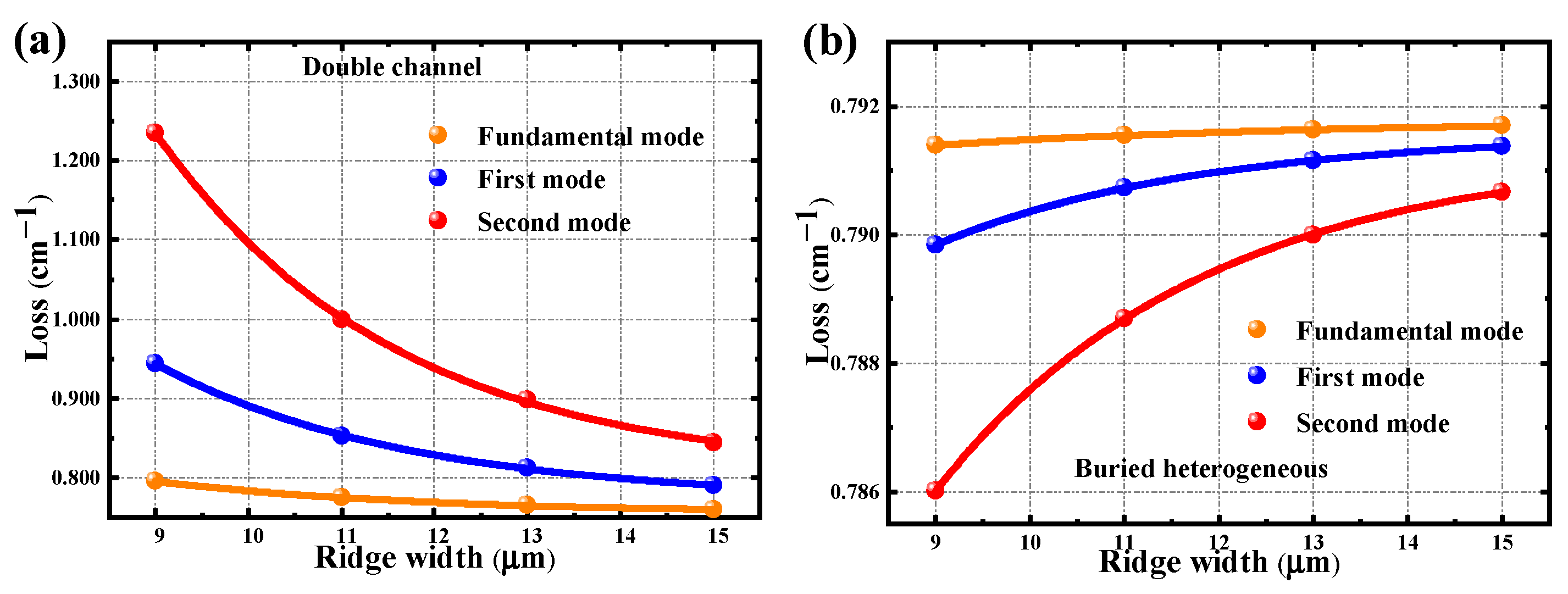
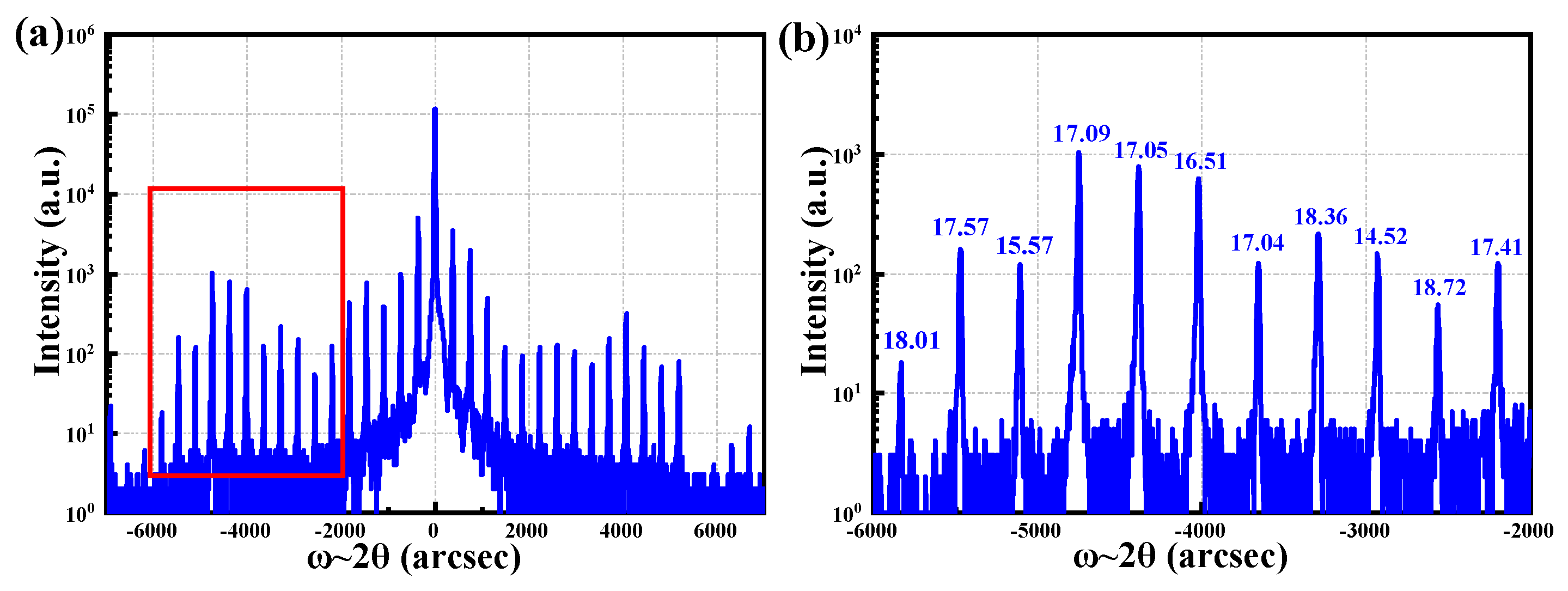
2.1. Structure Analysis

The adopted step taper active region structure (STA) is observed in ref. [23]; some optimized designs have also been carried out, mainly to optimize the composition of the material. The highly doped N-type InP substrate is used, and the active region is a strain-compensated InGaAs/InAlAs superlattice grown alternately by multiple components. Starting from the substrate, the epitaxial layers are sequentially grown as follows: a 3.5 μm InP lower cladding layer, a 0.1 μm InGaAs confinement layer, 40 periods of the InGaAs/InAlAs active region, the thickness of the active region is about 2 μm, a 0.1 μm InGaAs confinement layer, a 3 μm low-doped InP waveguide layer, and a 1 μm thick highly doped InP waveguide layer, as shown in Figure 1. After that, Si3N4 (300 nm) is grown by plasma-enhanced chemical vapor deposition (PECVD) as an electrical insulation layer. The surface is sputtered with a Ti/Pt/Au layer and annealed for ohmic contact. A thick gold layer of 4μm is electroplated to increase heat dissipation. The Ge/Au/Ni/Au (40 nm/250 nm/10 nm/250 nm) layer is steamed as the back electrode.
The step taper active region can not only suppress the leakage of high-energy carriers but also satisfy the rapid extraction of low-energy carriers so that the efficiency of population inversion is improved [29]. The calculated energy difference E54 can reach about 98 meV, which is much higher than the 50 meV of the traditional QCL. Therefore, the adopted STA can achieve higher internal quantum efficiency. On the other hand, the flow rate of the MOCVD source is linearly adjusted with a flow meter, making it easy to grow multiple components and combine them to form a more flexible active region structure, so the STA is suitable for MOCVD growth [30].
It is a challenge to achieve high outout power in QCL. One of the most direct ways is to increase the volume of the active region. There are primarily three methods to achieve this: increasing the number of active regions, increasing cavity length, and increasing ridge width. These methods aim to increase the optical confinement factor. In this study, the focus is to optimize and modify ridge width to improve its performance. For comparison, two different device structures are prepared in Figure 2: the double-channel ridge structure (DC) and the buried heterogeneous structure (BH). The mode loss of the two structures with different ridge widths are simulated, as shown in Figure 2a,b. The simulation result of BH structural mode loss is similar to ref. [31]. As shown in Figure 2a,b, the mode loss of the DC structure is higher than that of the BH structure. At the same time, the increase in the ridge width of the DC structure leads to the decrease in mode loss, and the loss of a high-order mode is much higher than that of a fundamental mode, whereas the situation for the BH structure is opposite. This is because additional waveguide losses are provided by the metal and insulation layers that cover the etched channels, better confining high-order modes. As a result, the double-channel structure may provide output with a wide ridge and good beam quality [25]. In summary, the DC structure is more effective at achieving high beam quility with broader emitter width compared to the BH structure.
By regrowing Fe:InP, the buried heterogeneous structure improves the device’s lateral heat dissipation capability, but the complex preparation procedure for this structure leads to a limited yield. The double-channel ridge structure does not require further growth, the preparation process is relatively simple, the yield is high, and industrial production is easier to achieve. However, due to the low thermal conductivity of the insulating layer material covered by the double channel ridge structure sidewalls, the device’s longitudinal heat dissipation capability has to be enhanced. The DC device structure is shown in Figure 3a; the injected power density of the device is 2 × 10¹⁴ W/m3. Figure 3b shows that as the ridge width increases, the core temperature of the AlN heat sink device increases from 436 K to 467 K. Therefore, the wider ridge device reaches the thermal rollover point first. Two different high-thermal-conductivity heat sinks, AlN and diamond, are used to enhance the longitudinal heat dissipation capability of the device, with thermal conductivity coefficients of approximately 230 W·m−1·K−1 and 1800 W·m−1·K−1, respectively [32]. Figure 3b shows the impacts of the two packages on the double-channel ridge structure’s temperature performance. It is found that the active region temperature reduces by 6–10 K when utilizing a diamond heat sink compared to an AlN heat sink. Despite the fact that the device’s heat accumulation worsens as ridge width increases, high power output is still achievable because the device’s mode loss is gradually reduced and a heat sink with a higher thermal conductivity is employed to enhance the longitudinal heat dissipation capability of the double channel structure.

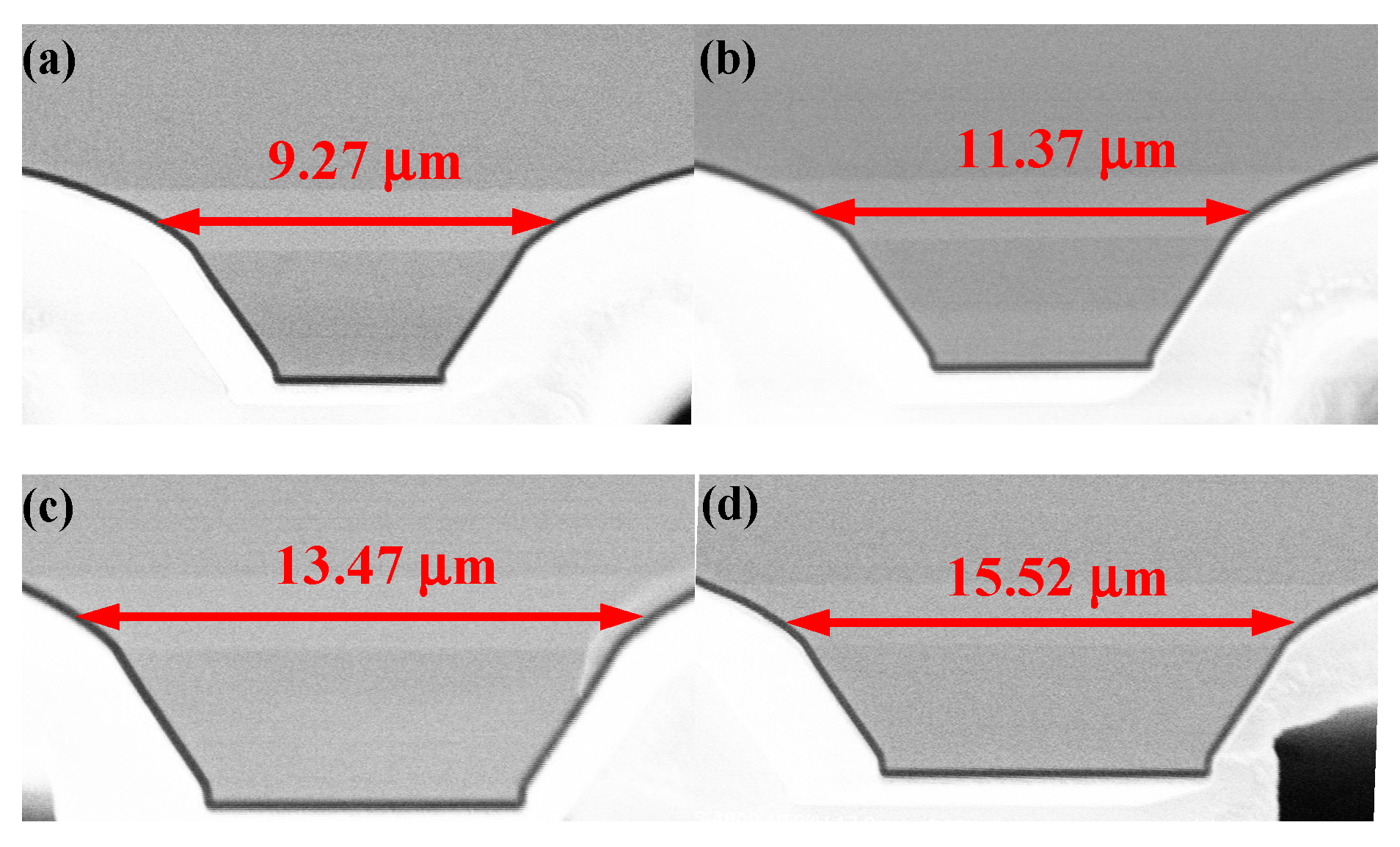
2.2. Device Fabrication

In the growth experiment, the entire epitaxial structure is grown by MOCVD (AIXTRON), and the reaction chamber adopts a close-coupled spray structure. After growth, the growth quality is characterized by the XRD. In Figure 4, it is observed from XRD images that the sample has a clear and sharp peak. The FWHM of the peaks of the sample is 14″~18″, indicating that the sample interface has a small roughness and good growth quality. The wafer is then processed into devices of different ridge widths. The ridge widths measured by SEM are 9.27 μm, 11.67 μm, 13.77 μm and 15.52 μm, respectively, as shown in Figure 5. The back cavity of the chips is coated with a high-reflectivity film. The chips are packed on AlN and make use of epilayer-down technology, which can improve the heat dissipation efficiency of active area.

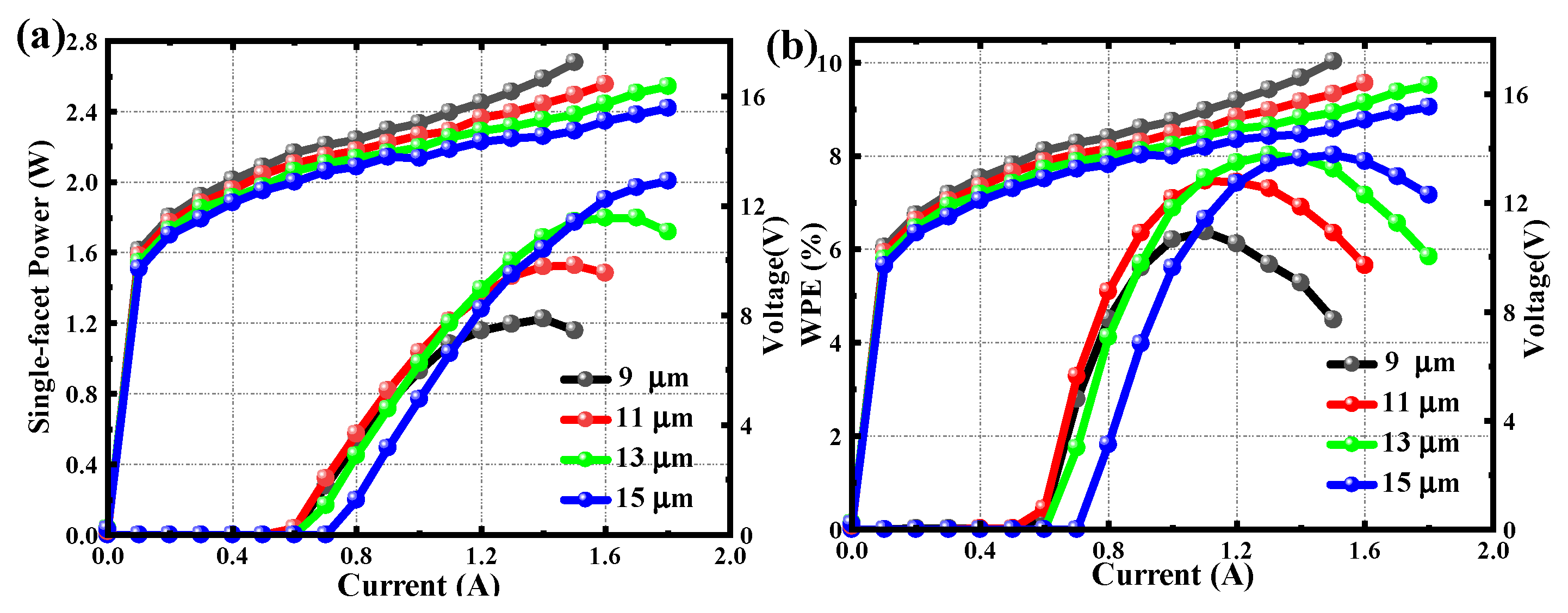
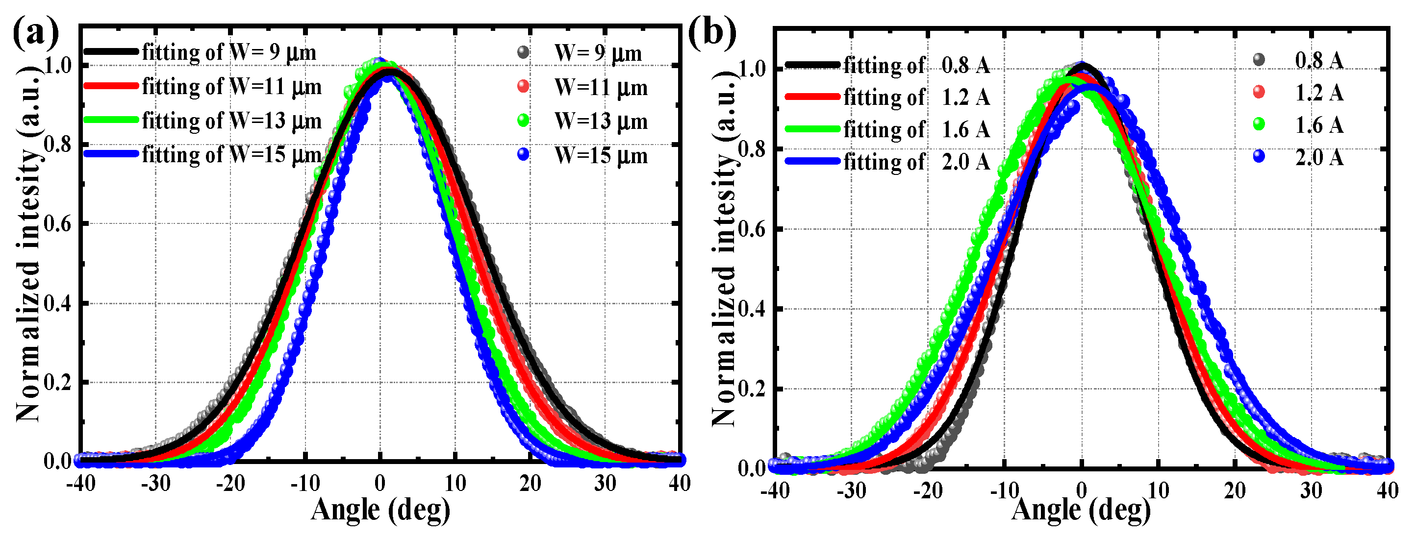
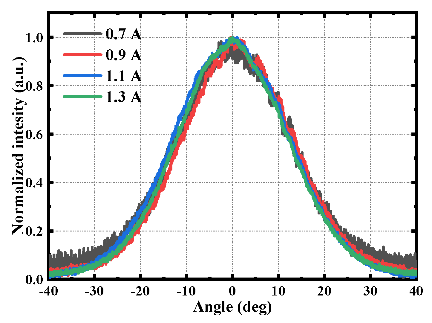
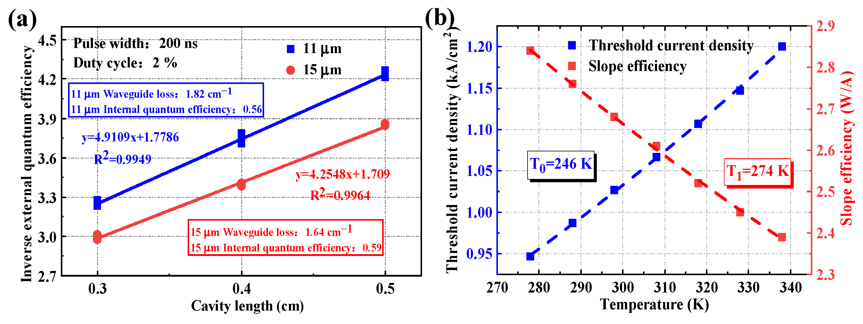
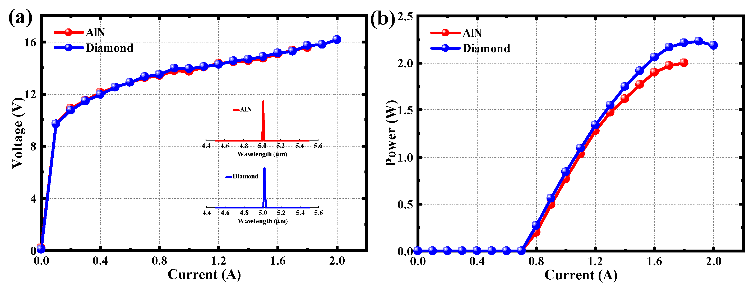
3. Device Performance and Testing

After packing, the tests are carried out at a temperature of 288 K under CW operation. The temperature is monitored by a thermistor and controlled by a thermoelectric cooler (TEC). Figure 6a,b are the L-I-V curve at different ridge widths and wall plug efficiency curves. The threshold current of the 9 μm device is 0.58 A. The slope efficiency is 2.29 W/A, the maximum output power is 1.23 W, and the maximum wall plug efficiency is 6.4%. The threshold current of the 11 μm device is 0.56 A. The slope efficiency is 2.53 W/A, the maximum output power is 1.52 W, and the maximum wall plug efficiency is 7.5%. The threshold current of the 13 μm device is 0.63 A. The slope efficiency is 2.60 W/A, the maximum output power is 1.80 W, and the maximum wall plug efficiency is 8.0%. The threshold current of the 15 μm device is 0.73 A. The slope efficiency is 2.70 W/A, the maximum output power is 2.00 W, and the maximum wall plug efficiency is 8.0%. In conclusion, the maximum output power and the maximum wall plug efficiency of the devices are both gradually increasing as the ridge width increases. This is caused by the increase in the volume of the active region. At the same time, the threshold current of the device gradually increases; this is due to the increase in the volume of the active region of the device that requires a higher level of current injection.
Figure 7 is the Power–Voltage–Current density curve. The threshold current densities of 9, 11, 13 and 15 μm devices are, respectively, 1.29 kA/cm2, 1.01 kA/cm2, 0.97 kA/cm2 and 0.97 kA/cm2. In Figure 8b, the rollover current density becomes smaller with a wider ridge width, because as the ridge width of the device increases, the heat accumulation of the device becomes more severe, so the thermal rollover point is be reached earlier.
Figure 8a shows the slow-axis far-field pictures of four devices measured at the same current density. The full width at half maxima (FWHMs) of the slow axes are 26.9°, 25.8°, 22.1°, and 18.7°, respectively. The beam quality of the four groups is kept great. Figure 6b shows the slow-axis far-field images measured by the 15 μm device at different currents. The FWHMs of the slow axis are 19.8°, 22.8°, 26.7°, and 27.2°, respectively. At the current of 2A, the slow-axis far-field divergence angle is only 27.2°, and the beam quality of the device remains good. It is found that as the current increases, the far field of the device gradually expands. This is attributed to the increase in the thermal effect caused by the increase in the current, the result of phase locking between the fundamental mode and the high-order mode, that is, the beam steering [33,34]. In summary, the simulation results are consistent with the experimental results.
Figure 9 shows the slow-axis far-field images measured by the 9 μm device at different currents. The FWHMs of the slow axis are 28.3°, 27.9°, 28.9° and 28.2°, respectively. The slow-axis divergence angle of the 9 μm device does not change significantly with different drive currents, which indicates that the mode of the 9 μm device is relatively stable and the beam steering is hardly observed. At this time, the mode loss of a high-order mode is much higher than that of the fundamental mode in the case of narrow ridge width, so the lasing of the high-order mode is relatively difficult.
The slow-axis far-field of BH structures at the same current density is measured. As the ridge width increases, the beam quality gradually deteriorates, leading to a significant high-order mode phenomenon, which is consistent with simulation. As a result, in order to ensure higher beam quality, thinner ridge widths for buried heterogeneous are required.
Figure 10a shows the relationship between the external quantum efficiency and the cavity length through the following calculation equations:
1 η e = 1 η i + 2 α i L η i ln 1 / R 1 R 2
It can be seen that the external quantum efficiency has a linear relationship with the cavity length, and the internal quantum efficiency and internal loss can be calculated by fitting the test results of the chips. The reflectance R1 of the uncoated cavity surface is 0.27, and the reflectance R2 of the highly reflective film is 0.99. The lasing wavelength of the device is 5 μm. The test conditions are a pulse width of 200 ns and a duty cycle of 2%. By testing and fitting data from multiple devices, internal quantum efficiency and internal loss data can be obtained. The internal quantum efficiency of the 11 μm ridge width device is 0.56, internal loss is 1.82 cm−1, and the internal quantum efficiency of the 15 μm ridge width device is 0.59 while internal loss is 1.64 cm−1. It is found that with the increase in the ridge width, the internal quantum efficiency of the device increases, and the internal loss decreases, so the performance of the device improves, which is consistent with the simulation. Figure 10b shows threshold current density and slope efficiency at different temperatures in pulse conditions at 200 ns, a 2% duty cycle. As the temperature increases, threshold current density increases and slope efficiency decreases. The experimental relationship is established according to the following equations:
J t h = J 0 exp T / T 0
η S = η 0 exp T / T 1
where T is the heat sink temperature. The characteristic temperatures, T0 and T1, in the pulsed operation are identified to be 246 K and 274 K, respectively. The higher T0 indicates that the leakage problem of carriers is significantly improved. The relatively low T1 is improved by reducing the overlap between the upper state E4 and the excited state E5 [35,36].
In addition, to achieve better performance, the chips are packaged on the diamond to improve its vertical heat dissipation capability. Figure 11 is a comparison between a diamond heat sink and an AlN heat sink device, and the insert figure shows the spectra of both. From the figure, it is found that the maximum output power of the device of the diamond heat sink is about 0.2 W higher than that of the device of the AlN heat sink, and the wavelength is around 5 μm. The subtle differences in spectra may be caused by uneven growth.

4. Conclusions

In summary, to achieve a larger ridge width QCL output with high beam quality, a double-channel ridge structure device is adopted and the packaging process is optimized. In the meantime, the relationship between the ridge width of different structures and the modes is studied. At the same time, the relationship between ridge width and device performance is discussed. Through simulation, it is found that as the ridge width increases, the active region temperature of the device increases and the waveguide loss decreases. In the experiment, the device achieves optimal performance under the ridge width of 15 µm; a room temperature CW power up to 2.2 W with a maximum WPE of 6.1% is obtained, and the device maintains good beam quality until the saturation current. This paper achieves larger ridge width QCL output with high beam quality. In addition, the device shows that the threshold current is insensitive to temperature changes.

Author Contributions

Conceptualization, J.W., D.Z. and Y.W.; methodology, Y.C., Z.W., J.W. and Y.W.; software, Y.Z. and Y.W.; investigation, Y.C., Z.W., J.W. and Y.W.; writing—original draft preparation, Y.C., Y.Z., J.W., W.Z. and Y.W.; writing—review and editing, Y.C., Y.Z., J.W., W.Z. and Y.W.; visualization, Y.Z. and Y.W.; supervision, J.W., D.Z. and Y.C. All authors have read and agreed to the published version of the manuscript.

Funding

This work was supported by the National Key R&D Programs of China under Grant No. 2018YFB1107301.

Data Availability Statement

The data presented in this study are available on reasonable request from the corresponding author.

Acknowledgments

The authors thank Zhimin Liang for their help in device testing.

Conflicts of Interest

Authors Yupei Wang, Yuhang Zhang, Jun Wang, Yang Cheng, Wu Zhao and Zhixiang Wei were employed by the company Suzhou Everbright Photonics Co., Ltd. The remaining authors declare that the research was conducted in the absence of any commercial or financial relationships that could be construed as a potential conflict of interest.

References

  1. Faist, J.; Capasso, F.; Sivco, D.L.; Sirtori, C.; Hutchinson, A.L.; Cho, A.Y. Quantum cascade laser. Science 1994, 264, 553–556. [Google Scholar] [CrossRef] [PubMed]
  2. Vitiello, M.S.; Scalari, G.; Williams, B.; De Natale, P. Quantum cascade lasers: 20 years of challenges. Opt. Express 2015, 23, 5167–5182. [Google Scholar] [CrossRef] [PubMed]
  3. Fathololoumi, S.; Dupont, E.; Chan, C.W.I.; Wasilewski, Z.R.; Laframboise, S.R.; Ban, D.; Mátyás, A.; Jirauschek, C.; Hu, Q.; Liu, H.C. Terahertz quantum cascade lasers operating up to ∼200 K with optimized oscillator strength and improved injection tunneling. Opt. Express 2012, 20, 3866–3876. [Google Scholar] [CrossRef] [PubMed]
  4. Li, L.; Chen, L.; Zhu, J.; Freeman, J.; Dean, P.; Valavanis, A.; Davies, A.G.; Linfield, E.H. Terahertz quantum cascade lasers with >1 W output powers. Electron. Lett. 2014, 50, 309–311. [Google Scholar] [CrossRef]
  5. Spitz, O.; Didier, P.; Durupt, L.; Diaz-Thomas, D.A.; Baranov, A.N.; Cerutti, L.; Grillot, F. Free-space communication with directly modulated mid-infrared quantum cascade devices. IEEE J. Sel. Top. Quantum Electron. 2021, 28, 1200109. [Google Scholar] [CrossRef]
  6. Dely, H.; Bonazzi, T.; Spitz, O.; Rodriguez, E.; Gacemi, D.; Todorov, Y.; Pantzas, K.; Beaudoin, G.; Sagnes, I.; Li, L.; et al. 10 Gbit s−1 free space data transmission at 9 µm wavelength with unipolar quantum optoelectronics. Laser Photonics Rev. 2022, 16, 2100414. [Google Scholar] [CrossRef]
  7. Cheng, F.; Zhang, J.; Guan, Y.; Yang, P.; Zhuo, N.; Zhai, S.; Liu, J.; Wang, L.; Liu, S.; Liu, F.; et al. Ultralow power consumption of a quantum cascade laser operating in continuous-wave mode at room temperature. Opt. Express 2020, 28, 36497–36504. [Google Scholar] [CrossRef]
  8. Wang, Z.; Kapsalidis, F.; Wang, R.; Beck, M.; Faist, J. Ultra-low threshold lasing through phase front engineering via a metallic circular aperture. Nat. Commun. 2022, 13, 230. [Google Scholar] [CrossRef]
  9. Cheng, F.; Zhang, J.; Sun, Y.; Zhuo, N.; Zhai, S.; Liu, J.; Wang, L.; Liu, S.; Liu, F. High performance distributed feedback quantum cascade laser emitting at λ∼6.12 um. Opt. Express 2022, 30, 5848–5854. [Google Scholar] [CrossRef]
  10. Fei, T.; Zhai, S.; Zhang, J.; Zhuo, N.; Liu, J.; Wang, L.; Liu, S.; Jia, Z.; Li, K.; Sun, Y.; et al. High power λ~ 8.5 μm quantum cascade laser grown by MOCVD operating continuous-wave up to 408 K. J. Semicond. 2021, 42, 112301. [Google Scholar] [CrossRef]
  11. Wang, H.; Zhang, J.; Cheng, F.; Zhuo, N.; Zhai, S.; Liu, J.; Wang, L.; Liu, S.; Liu, F.; Wang, Z. Watt-level, high wall plug efficiency, continuous-wave room temperature quantum cascade laser emitting at 7.7 µm. Opt. Express 2020, 28, 40155–40163. [Google Scholar] [CrossRef]
  12. Zhou, W.; Lu, Q.Y.; Wu, D.H.; Slivken, S.; Razeghi, M. High-power, continuous-wave, phase-locked quantum cascade laser arrays emitting at 8 µm. Opt. Express 2019, 27, 15776–15785. [Google Scholar] [CrossRef]
  13. Beck, M.; Hofstetter, D.; Aellen, T.; Faist, J.; Oesterle, U.; Ilegems, M.; Gini, E.; Melchior, H. Continuous wave operation of a mid-infrared semiconductor laser at room temperature. Science 2002, 295, 301–305. [Google Scholar] [CrossRef] [PubMed]
  14. Bai, Y.; Darvish, S.R.; Slivken, S.; Zhang, W.; Evans, A.; Nguyen, J.; Razeghi, M. Room temperature continuous wave operation of quantum cascade lasers with watt-level optical power. Appl. Phys. Lett. 2008, 92, 101105. [Google Scholar] [CrossRef]
  15. Lyakh, A.; Maulini, R.; Tsekoun, A.; Go, R.; Pflügl, C.; Diehl, L.; Wang, Q.J.; Capasso, F.; Patel, C.K.N. 3 W continuous-wave room temperature single-facet emission from quantum cascade lasers based on nonresonant extraction design approach. Appl. Phys. Lett. 2009, 95, 141113. [Google Scholar] [CrossRef]
  16. Wang, F.; Slivken, S.; Wu, D.H.; Lu, Q.Y.; Razeghi, M. Continuous wave quantum cascade lasers with 5.6 W output power at room temperature and 41% wall-plug efficiency in cryogenic operation. AIP Adv. 2020, 10, 055120. [Google Scholar] [CrossRef]
  17. Patel, C.K.N.; Troccoli, M.; Barron-Jimenez, R.; Titterton, D.H.; Grasso, R.J.; Richardson, M.A. Quantum cascade lasers: 25 years after the first demonstration. In Technologies for Optical Countermeasures XVI; SPIE: Bellingham, WA, USA, 2019. [Google Scholar]
  18. Diehl, L.; Bour, D.; Corzine, S.; Zhu, J.; Höfler, G.; Lončar, M.; Troccoli, M.; Capasso, F. High-temperature continuous wave operation of strain-balanced quantum cascade lasers grown by metal organic vapor-phase epitaxy. Appl. Phys. Lett. 2006, 89, 081101. [Google Scholar] [CrossRef]
  19. Diehl, L.; Bour, D.; Corzine, S.; Zhu, J.; Höfler, G.; Lončar, M.; Troccoli, M.; Capasso, F. High-power quantum cascade lasers grown by low-pressure metal organic vapor-phase epitaxy operating in continuous wave above 400 K. Appl. Phys. Lett. 2006, 88, 201115. [Google Scholar] [CrossRef]
  20. Troccoli, M.; Diehl, L.; Bour, D.P.; Corzine, S.W.; Yu, N.; Wang, C.Y.; Belkin, M.A.; Höfler, G.; Lewicki, R.; Wysocki, G.; et al. High-performance quantum cascade lasers grown by metal-organic vapor phase epitaxy and their applications to trace gas sensing. J. Light. Technol. 2008, 26, 3534–3555. [Google Scholar] [CrossRef]
  21. Wang, C.A.; Huang, R.K.; Sanchez-Rubio, A.; Goyal, A.; Donnelly, J.P.; Calawa, D.R.; Cann, S.G.; O’Donnell, F.; Plant, J.J.; Missaggia, L.J.; et al. OMVPE growth of highly strain-balanced GaInAs/AlInAs/InP for quantum cascade lasers. J. Cryst. Growth 2008, 310, 5191–5197. [Google Scholar] [CrossRef]
  22. Roberts, J.S.; Green, R.P.; Wilson, L.R.; Zibik, E.A.; Revin, D.G.; Cockburn, J.W.; Airey, R.J. Quantum cascade lasers grown by metalorganic vapor phase epitaxy. Appl. Phys. Lett. 2003, 82, 4221–4223. [Google Scholar] [CrossRef]
  23. Botez, D.; Kirch, J.D.; Boyle, C.; Oresick, K.M.; Sigler, C.; Kim, H.; Knipfer, B.B.; Ryu, J.H.; Lindberg, D.; Earles, T.; et al. High-efficiency, high-power mid-infrared quantum cascade lasers. Opt. Mater. Express 2018, 8, 1378–1398. [Google Scholar] [CrossRef]
  24. Fei, T.; Zhai, S.; Zhang, J.; Lu, Q.; Zhuo, N.; Liu, J.; Wang, L.; Liu, S.; Jia, Z.; Li, K.; et al. 3 W Continuous-Wave Room Temperature Quantum Cascade Laser Grown by Metal-Organic Chemical Vapor Deposition. Photonics 2023, 10, 47. [Google Scholar] [CrossRef]
  25. Bouzi, P.M. High Performance Quantum Cascade Lasers: Loss, Beam Stability, and Gain Engineering. Ph.D. Thesis, Princeton University, Princeton, NJ, USA, 2015; p. 142. [Google Scholar]
  26. Bouzi, P.M.; Liu, P.Q.; Aung, N.; Wang, X.; Fan, J.-Y.; Troccoli, M.; Gmachl, C.F. Suppression of pointing instability in quantum cascade lasers by transverse mode control. Appl. Phys. Lett. 2013, 102, 122105. [Google Scholar] [CrossRef]
  27. Lu, Q.Y.; Bai, Y.; Bandyopadhyay, N.; Slivken, S.; Razeghi, M. Room-temperature continuous wave operation of distributed feedback quantum cascade lasers with watt-level power output. Appl. Phys. Lett. 2010, 97, 231119. [Google Scholar] [CrossRef]
  28. Lu, Q.Y.; Bai, Y.; Bandyopadhyay, N.; Slivken, S.; Razeghi, M. 2.4 W room temperature continuous wave operation of distributed feedback quantum cascade. Appl. Phys. Lett. 2011, 98, 181106. [Google Scholar] [CrossRef]
  29. Bai, Y.; Bandyopadhyay, N.; Tsao, S.; Selcuk, E.; Slivken, S.; Razeghi, M. Highly temperature insensitive quantum cascade lasers. Appl. Phys. Lett. 2010, 97, 251104. [Google Scholar] [CrossRef]
  30. Lei, P.; Cheng, Y.; Zhao, W.; Tan, S.; Guo, Y.; Li, B.; Wang, J.; Zhou, D. Mid-infrared quantum cascade laser grown by MOCVD at 4.6 µm. Infrared Laser Eng. 2022, 51, 20210980. [Google Scholar]
  31. Ryu, J.H.; Kirch, J.D.; Knipfer, B.; Liu, Z.; Turville-Heitz, M.; Earles, T.; Marsland, R.A.; Strömberg, A.; Omanakuttan, G.; Sun, Y.-T.; et al. Beam stability of buried-heterostructure quantum cascade lasers employing HVPE regrowth. Opt. Express 2021, 29, 2819–2826. [Google Scholar] [CrossRef]
  32. Evans, A.J. GasMBE Growth and Characterization of Strained Layer Indium Phosphide-Gallium Indium Arsenide-Aluminum Indium Arsenide Quantum Cascade Lasers. Ph.D. Thesis, Northwestern University, Evanston, IL, USA, 2008; p. 326. [Google Scholar]
  33. Bewley, W.W.; Lindle, J.R.; Kim, C.S.; Vurgaftman, I.; Meyer, J.R.; Evans, A.J.; Yu, J.S.; Slivken, S.; Razeghi, M. Beam steering in high-power CW quantum-cascade lasers. IEEE J. Quantum Electron. 2005, 41, 833–841. [Google Scholar] [CrossRef]
  34. Bai, Y. High Wall Plug Efficiency Quantum Cascade Lasers. Ph.D. Thesis, Northwestern University, Evanston, IL, USA, 2011; p. 275. [Google Scholar]
  35. Lyakh, A.; Suttinger, M.; Go, R.; Figueiredo, P.; Todi, A. 5.6 μm quantum cascade lasers based on a two-material active region composition with a room temperature wall-plug efficiency exceeding 28%. Appl. Phys. Lett. 2016, 109, 121109. [Google Scholar] [CrossRef]
  36. Sun, Y.; Yin, R.; Zhang, J.; Liu, J.; Fei, T.; Li, K.; Guo, K.; Jia, Z.; Liu, S.; Lu, Q.; et al. High-performance quantum cascade lasers at λ∼9 µm grown by MOCVD. Opt. Express 2022, 30, 37272–37280. [Google Scholar] [CrossRef] [PubMed]
Figure 1. Layers sequence and doping.
Photonics 11 00214 g001
Figure 2. (a) Double channel mode loss with different ridge widths; (b) Buried heterogeneous structure mode loss with different ridge widths.
Photonics 11 00214 g002
Figure 3. (a) Device structure diagram; (b) Working temperature for different ridge widths and different heat sinks.
Photonics 11 00214 g003
Figure 4. (a) X-ray double crystal diffraction of sample ω~(2θ) test result; (b) X-ray double crystal diffraction of sample ω~(2θ). Enlarged view of test results (red box).
Photonics 11 00214 g004
Figure 5. The ridge width of the samples. (a) 9 μm device; (b) 11 μm device; (c) 13 μm device; (d) 15 μm device.
Photonics 11 00214 g005
Figure 6. (a) Power–Voltage–Current curve under different ridge widths; (b) the WPE curve under different ridge widths.
Photonics 11 00214 g006
Figure 7. Power–Voltage–Current density curve under different ridge widths.
Photonics 11 00214 g007
Figure 8. (a) Far–field of devices with different ridge widths at the same current density; (b) Far–field of devices with different currents at the 15 μm ridge width.
Photonics 11 00214 g008
Figure 9. Far–field of devices with different currents at the 9 μm ridge width.
Photonics 11 00214 g009
Figure 10. Relationship between external quantum efficiency and cavity length. (a) Internal quantum efficiency fitting; (b) Characteristic temperature fitting.
Photonics 11 00214 g010
Figure 11. (a) I-V of AlN heat sink devices and diamond heat sink device. The insert figure shows the spectra of both. (b) L-I of AlN heat sink devices and diamond heat sink device.
Photonics 11 00214 g011
Disclaimer/Publisher’s Note: The statements, opinions and data contained in all publications are solely those of the individual author(s) and contributor(s) and not of MDPI and/or the editor(s). MDPI and/or the editor(s) disclaim responsibility for any injury to people or property resulting from any ideas, methods, instructions or products referred to in the content.

