Saturated Gain-Induced Non-Reciprocal Transmission and Broadband On-Chip Optical Isolator

Abstract
:1. Introduction
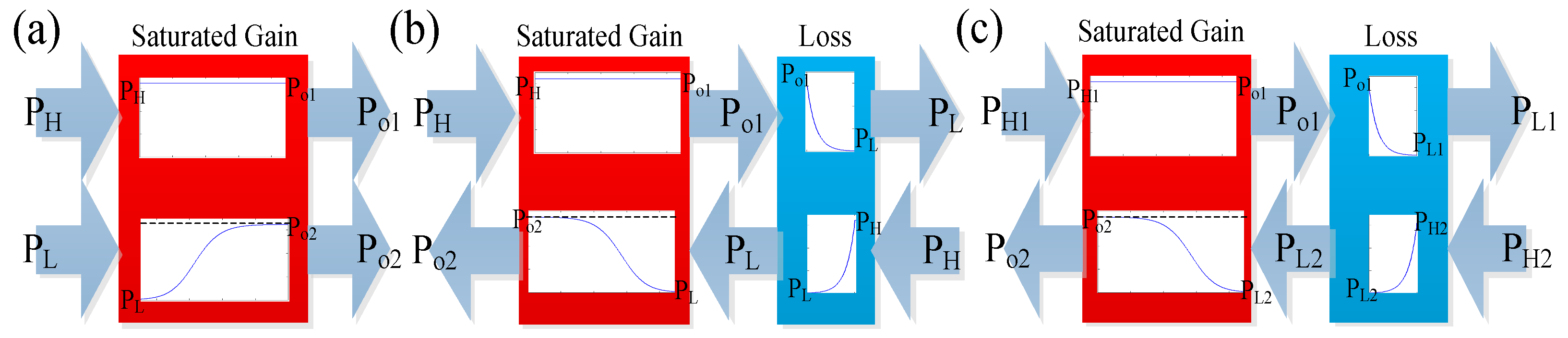
2. Non-Reciprocal Transmission in Saturated Gain Waveguide
3. Isolator Model
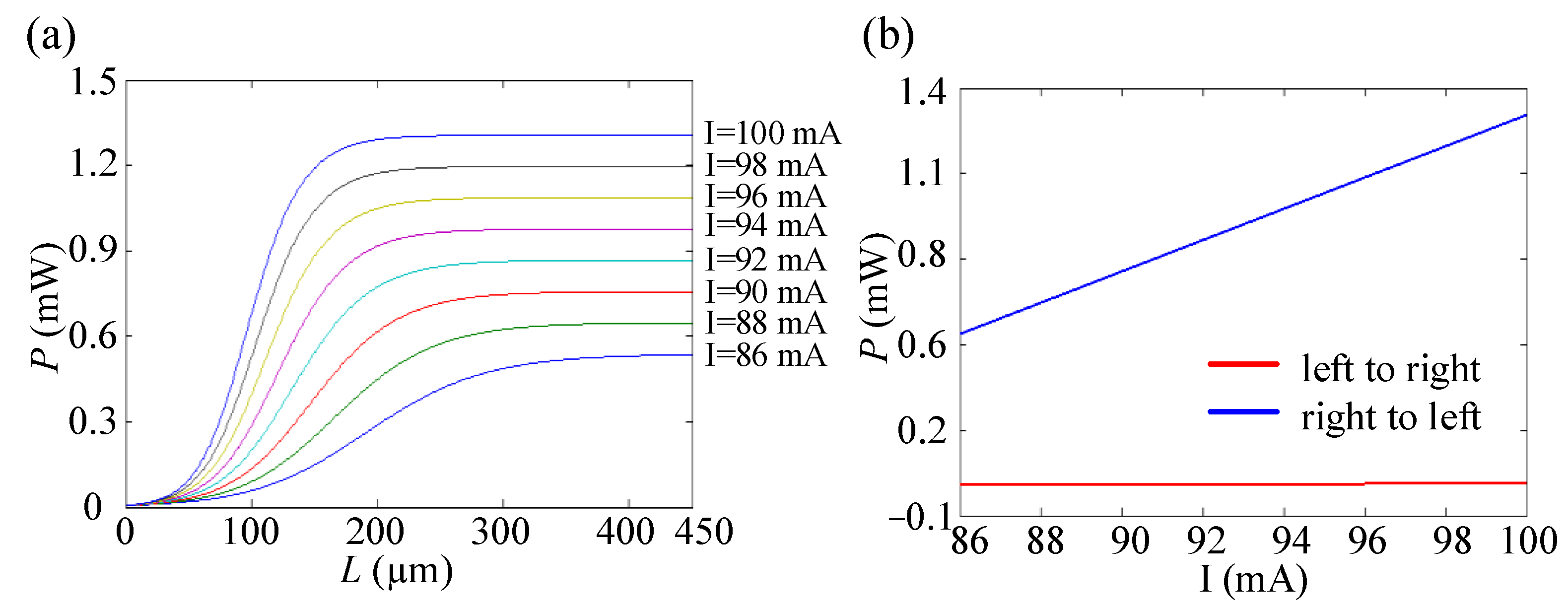
4. Device Designing
5. Conclusions
Author Contributions
Funding
Institutional Review Board Statement
Informed Consent Statement
Data Availability Statement
Conflicts of Interest
References
- Ma, H.; He, Z.; Hotate, K. Reduction of backscattering induced noise by carrier suppression in waveguide-type optical ring resonator. J. Light. Technol. 2011, 29, 85–90. [Google Scholar] [CrossRef]
- Zhang, Z.; Zhu, L. Nonreciprocal thermal photonics for energy conversion and radiative heat transfer. Phys. Rev. Appl. 2022, 18, 027001. [Google Scholar] [CrossRef]
- Shui, T.; Yang, W.X.; Cheng, M.T.; Lee, R.K. Optical nonreciprocity and nonreciprocal photonic devices with directional four-wave mixing effect. Opt. Express 2022, 30, 6284–6299. [Google Scholar] [CrossRef] [PubMed]
- Ehlers, P.; Silander, I.; Wang, J.; Foltynowicz, A.; Axner, O. Fiber-laser-based noise-immune cavity-enhanced optical heterodyne molecular spectrometry incorporating an optical circulator. Opt. Lett. 2014, 39, 279–282. [Google Scholar] [CrossRef]
- Wang, X.; Hao, R.; Fan, P.; Hu, L.; Ye, B.; Zou, Y.; Jin, S. Effective enhancement of the non-Hermitian corner skin effect in reciprocal photonic crystals. Opt. Lett. 2024, 49, 554–557. [Google Scholar] [CrossRef] [PubMed]
- He, H.; Zhang, S.; Qi, J.; Bo, F.; Li, H. Faraday rotation in nonreciprocal photonic time-crystals. Appl. Phys. Lett. 2023, 122, 051703. [Google Scholar] [CrossRef]
- Mimbs, J.W.; O’Donnell, M.; Miller, J.G.; Sobel, B.E. Detection of cardiomyopathic changes induced by doxorubicin based on quantitative analysis of ultrasonic backscatter. Am. J. Cardiol. 1981, 47, 1056–1060. [Google Scholar] [CrossRef]
- Dong, C.; Shen, Z.; Zou, C.; Zhang, Y.; Fu, W.; Guo, G. Non-reciprocal light storage in a silica microsphere. In Proceedings of the 2015 Conference on Lasers and Electro-Optics (CLEO), San Jose, CA, USA, 10–15 May 2015; pp. 1–2. [Google Scholar]
- Zheng, Y.; Yang, J.; Shen, Z.; Cao, J.; Chen, X.; Liang, X.; Wan, W. Optically induced transparency in a micro-cavity. Light Sci. Appl. 2016, 5, e16072. [Google Scholar] [CrossRef]
- Chang, L.; Jiang, X.; Hua, S.; Yang, C.; Wen, J.; Jiang, L.; Li, G.; Wang, G.; Xiao, M. Parity–time symmetry and variable optical isolation in active-passive-coupled microresonators. Nat. Photonics 2014, 8, 524–529. [Google Scholar] [CrossRef]
- Ahmed, W.; Farhat, M.; Staliunas, K.; Zhang, X.; Wu, Y. Machine learning for knowledge acquisition and accelerated inverse-design for non-Hermitian systems. Commun. Phys. 2023, 6, 2. [Google Scholar] [CrossRef]
- Peng, B.; Özdemir, Ş.; Lei, F.; Monifi, F.; Gianfreda, M.; Long, G.; Fan, S.; Nori, F.; Bender, C.; Yang, L. Parity–time-symmetric whispering-gallery microcavities. Nat. Phys. 2014, 10, 394–398. [Google Scholar] [CrossRef]
- Shen, Z.; Dong, C.; Chen, Y.; Xiao, Y.; Sun, F.; Guo, G. Compensation of the Kerr effect for transient optomechanically induced transparency in a silica microsphere. Opt. Lett. 2016, 41, 1249–1252. [Google Scholar] [CrossRef] [PubMed]
- Bi, L.; Hu, J.; Jiang, P.; Kim, D.; Dionne, G.; Kimerling, L.; Ross, C. On-chip optical isolation in monolithically integrated non-reciprocal optical resonators. Nat. Photonics 2011, 5, 758–762. [Google Scholar] [CrossRef]
- Tian, H.; Liu, J.; Siddharth, A.; Wang, R.; Blésin, T.; He, J.; Kippenberg, T.; Bhave, S. Magnetic-free silicon nitride integrated optical isolator. Nat. Photonics 2021, 15, 828–836. [Google Scholar] [CrossRef]
- Kittlaus, E.; Jones, W.; Rakich, P.; Otterstrom, N.; Muller, R.; Rais-Zadeh, M. Electrically driven acousto-optics and broadband non-reciprocity in silicon photonics. Nat. Photonics 2021, 15, 43–52. [Google Scholar] [CrossRef]
- Wang, C.; Fu, Z.; Mao, W.; Qie, J.; Stone, A.; Yang, L. Non-Hermitian optics and photonics: From classical to quantum. Adv. Opt. Photonics 2023, 15, 442–523. [Google Scholar] [CrossRef]
- Fujita, J.; Levy, M.; Osgood Jr, R.; Wilkens, L.; Dötsch, H. Waveguide optical isolator based on Mach–Zehnder interferometer. Appl. Phys. Lett. 2000, 76, 2158–2160. [Google Scholar] [CrossRef]
- Vanwolleghem, M.; Gogol, P.; Beauvillain, P.; Van Parys, W.; Baets, R. Design and optimization of a monolithically integratable InP-based optical waveguide isolator. JOSA B 2007, 24, 94–105. [Google Scholar] [CrossRef]
- Van Parys, W.; Moeyersoon, B.; Van Thourhout, D.; Baets, R.; Vanwolleghem, M.; Dagens, B.; Decobert, J.; Le Gouezigou, O.; Make, D.; Lagae, L. Transverse magnetic mode non reciprocal propagation in an amplifying AlGaInAs/InP optical waveguide isolator. Appl. Phys. Lett. 2006, 88, 071115. [Google Scholar] [CrossRef]
- Qin, J.; Deng, L.; Xie, J.; Tang, T.; Bi, L. Highly sensitive sensors based on magneto-optical surface plasmon resonance in Ag/CeYIG heterostructures. AIP Adv. 2015, 5, 017118. [Google Scholar] [CrossRef]
- Shui, K.; Nie, L.; Zhang, Y.; Peng, B.; Xie, J.; Deng, L.; Bi, L. Design of a compact waveguide optical isolator based on multimode interferometers using magneto-optical oxide thin films grown on silicon-on-insulator substrates. Opt. Express 2016, 24, 12856–12867. [Google Scholar] [CrossRef] [PubMed]
- Yu, Z.; Fan, S. Complete optical isolation created by indirect interband photonic transitions. Nat. Photonics 2009, 3, 91–94. [Google Scholar] [CrossRef]
- Shen, Z.; Zhang, Y.; Chen, Y.; Zou, C.; Xiao, Y.; Zou, X.; Sun, F.; Guo, G.; Dong, C. Experimental realization of optomechanically induced non-reciprocity. Nat. Photonics 2016, 10, 657–661. [Google Scholar] [CrossRef]
- Galiffi, E.; Tirole, R.; Yin, S.; Li, H.; Vezzoli, S.; Huidobro, P.; Silveirinha, M.; Sapienza, R.; Alù, A.; Pendry, J. Photonics of time-varying media. Adv. Photonics 2022, 4, 014002. [Google Scholar] [CrossRef]
- Shi, Y.; Yu, Z.; Fan, S. Limitations of nonlinear optical isolators due to dynamic reciprocity. Nat. Photonics 2015, 9, 388–392. [Google Scholar] [CrossRef]
- Palik, E.D. Handbook of Optical Constants of Solids; Academic Press: New York, NY, USA, 1998. [Google Scholar]
- Dutta, N.K.; Wang, Q. Semiconductor Optical Amplifiers; World Scientific Press: Singapore, 2013. [Google Scholar]
- Sugawara, M.; Mukai, K.; Nakata, Y.; Ishikawa, H.; Sakamoto, A. Effect of homogeneous broadening of optical gain on lasing spectra in self-assembled InxGa1-xAs/GaAs quantum dot lasers. Phys. Rev. B 2000, 61, 7595. [Google Scholar] [CrossRef]
- Durhuus, T.; Mikkelsen, B.; Stubkjaer, K. Detailed Dynamic Model for Semiconductor Optical Amplifiers and Their Crosstalk and Intermodulation Distortion. J. Light. Technol. 1992, 10, 1056–1065. [Google Scholar] [CrossRef]
- Connelly, M.J. Semiconductor Optical Amplifiers; Springer Science & Business Media: Berlin/Heidelberg, Germany, 2007. [Google Scholar]
- Sullivan, D.M. Electromagnetic Simulation Using the FDTD Method; John Wiley & Sons: Hoboken, NJ, USA, 2013. [Google Scholar]
- Available online: www.photond.com (accessed on 1 October 2020).


| Fabrication | Duplex Working | Operating Band | Size | |
|---|---|---|---|---|
| NLO | Easy | No | Narrow (~1 nm) | ~100 μm |
| MO micro-ring | Very Hard | Yes | Narrow (<1 nm) | ~100 μm |
| Normal MO | Easy | Yes | Wide (>50 nm) | >1 mm |
| TDO | Hard | Yes | Narrow (<10 nm) | ~100 μm |
| Saturated gain | Easy | Yes | Wide (>50 nm) | ~500 μm |
Disclaimer/Publisher’s Note: The statements, opinions and data contained in all publications are solely those of the individual author(s) and contributor(s) and not of MDPI and/or the editor(s). MDPI and/or the editor(s) disclaim responsibility for any injury to people or property resulting from any ideas, methods, instructions or products referred to in the content. |
© 2024 by the authors. Licensee MDPI, Basel, Switzerland. This article is an open access article distributed under the terms and conditions of the Creative Commons Attribution (CC BY) license (https://creativecommons.org/licenses/by/4.0/).
Share and Cite
Xue, M.; Tong, H.; Dong, H.; Wang, M. Saturated Gain-Induced Non-Reciprocal Transmission and Broadband On-Chip Optical Isolator. Photonics 2024, 11, 261. https://doi.org/10.3390/photonics11030261
Xue M, Tong H, Dong H, Wang M. Saturated Gain-Induced Non-Reciprocal Transmission and Broadband On-Chip Optical Isolator. Photonics. 2024; 11(3):261. https://doi.org/10.3390/photonics11030261
Chicago/Turabian StyleXue, Mingyuan, Haojiang Tong, Hao Dong, and Meijia Wang. 2024. "Saturated Gain-Induced Non-Reciprocal Transmission and Broadband On-Chip Optical Isolator" Photonics 11, no. 3: 261. https://doi.org/10.3390/photonics11030261