1. Introduction
In light of recent increases in data traffic spurred by digital transformation and the advent of 6G mobile communication networks, there is a growing demand for more advanced optical multiplexing technologies like wavelength division multiplexing (WDM) or coherent phase modulation techniques, particularly in datacenter applications [
1,
2,
3,
4,
5,
6,
7,
8,
9]. Silicon photonics stands out as a highly promising technological platform for the development of photonic integrated circuits (PICs) characterized by high bandwidth and low energy consumption. Considering silicon-based PICs [
8,
9,
10,
11,
12,
13,
14,
15], together with several photonic components such as laser diodes, optical modulators, and photodetectors, optical waveguide type demultiplexers (DeMUXs) such as microring resonators [
16,
17,
18,
19], delayed interferometers (DIs) [
20,
21,
22,
23,
24,
25,
26,
27,
28,
29,
30,
31,
32,
33,
34,
35,
36], or arrayed waveguide gratings (AWGs) [
37,
38,
39,
40,
41,
42,
43,
44,
45,
46,
47,
48] are normally needed to filter the WDM optical signals spatially out to each photodetector to be decoded.
Various WDM specifications, such as dense WDM (DWDM) and coarse WDM (CWDM), have emerged based on factors like channel count, channel spacing, and channel grid. Given that the DeMUX must cling to these specific requisites to function effectively as a spatial wavelength filter, its configuration needs optimization for each WDM specification. Additionally, concerning optical receivers, the polarization state of signals passing through standard single-mode fibers (SMFs) is not preserved upon coupling to each receiver end. Consequently, an optical DeMUX located on the receiver end becomes essential for handling arbitrarily polarized optical signals [
18,
30,
38,
40,
42,
49,
50,
51,
52]. Several approaches have been devised to address WDM signals at the receiver end, including depolarized [
28,
30,
40] or polarization diversity schemes [
35,
36,
47,
49].
This paper provides an overview of three silicon-nanowire-type DI-based optical DeMUXs tailored for datacenter applications: (1) a 100-GHz-spaced 16λ DWDM optical DeMUX [
49], (2) an 800-GHz-spaced 8λ long reach 8 (LR-8) optical DeMUX [
34], and (3) a 20-nm-spaced 4λ CWDM optical DeMUX [
35,
36]. We explore their functional advantages and identify technical aspects warranting further investigation compared to previous works.
Section 2 is devoted to describing the silicon-nanowire-based polarization splitter-rotator (PSR) responsible for handling arbitrary polarization input signals.
Section 3 presents the device scheme, operational principles, and experimental characterizations of the 100-GHz-spaced 16λ DWDM optical DeMUX.
Section 4 focuses on theoretical discussions regarding the 800-GHz-spaced 8λ LR-8 optical DeMUX.
Section 5 addresses the 20-nm-spaced 4λ CWDM optical DeMUX, particularly examining insertion loss (IL) and polarization crosstalk.
2. Silicon-Nanowire-Based PSR for Polarization Diversity
Typically, a silicon-nanowire waveguide exhibits a compressed core shape, resulting in significant structural birefringence [
35,
53,
54]. This relatively high birefringence enhances the efficiency of polarization diversity [
35,
36,
49] compared to alternative methods such as birefringence elimination [
28] or birefringence compensation [
30,
40]. Illustrated in
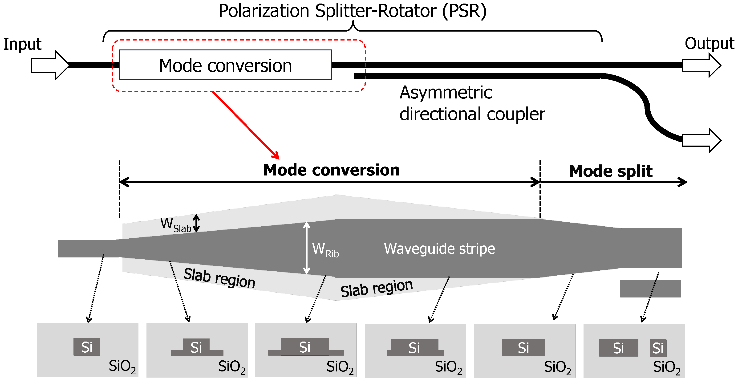
Figure 1 is a schematic depiction of the silicon-nanowire-based polarization splitter-rotator (PSR) for polarization diversity operation at the receiver end. The PSR comprises a hybrid mode conversion region utilizing rib-shaped silicon-nanowire waveguides [
35,
51,
52] and a mode split region employing a rectangle-shaped silicon-nanowire asymmetric directional coupler (ADC). It is established that the ADC enables randomly linear-polarization (i.e., the linear mixing of TE
00 and TM
00 modes) to separate into two outputs with TE
00 fundamental modes [
51,
52]. In Ref. [
51], normally, shallow-etched rib and normal channel waveguides are utilized for the PSR based on hybrid mode conversion. Such a waveguide shape can be readily fabricated using the currently available complementary metal–oxide–semiconductor (CMOS) foundry process [
55].
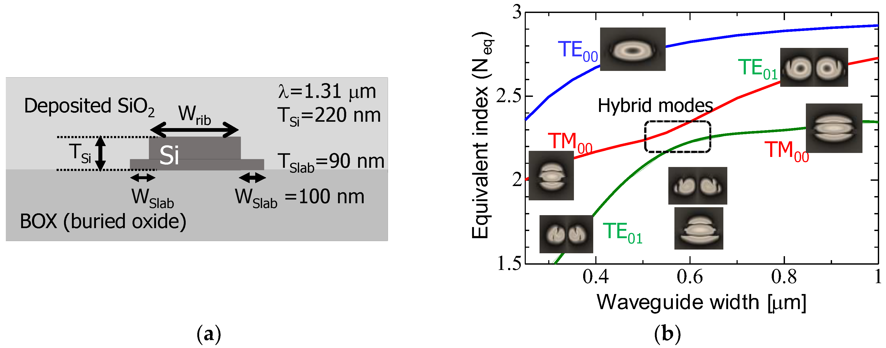
Figure 2 depicts the simulated propagation mode characteristics: (a) the cross-section view of the low etched silicon-nanowire waveguide and (b) the simulated equivalent refractive indices (N
eq) for typical propagation modes in the silicon-nanowire waveguide shown in (a) against the width of waveguide stripe (W
rib). Packaged software based on a finite element method (FemSIM
TM; Synopsys, CA, USA) was used for implementing the numerical simulation shown in
Figure 2b. For the simulation model illustrated in
Figure 2a, the silicon core thickness (T
Si), thin layer thickness (T
Slab), and thin layer width (W
Slab) were set to 220, 90, and 100 nm, respectively. As indicated in
Figure 2b, the mode profile continues to preserve as TE
00 mode irrespective of the value of W
rib, while the TM
00 mode undergoes hybrid mode states, exhibiting both polarizations from TM
00 mode to TE
01 higher mode at a certain W
rib of approximately 0.55 µm. That is, only the TM
00-mode state is coupled to the TE
01 mode by adiabatically changing the values of W
rib and W
Slab. We leverage this TM
00-to-TE
00-mode conversion to segregate the two input polarization modes into spatially distinct output channels. The number of modes displayed in
Figure 2b were restricted to three typical states. It should be noted that the contribution of other higher order modes can be neglected since the main two states of polarization are difficult to couple to any other higher order polarization states.
Meanwhile, as schematically shown in
Figure 1 and
Figure 2, the hybrid mode conversion within the PSR needs the shallow-etched rib waveguide structure whose slab width is properly defined. Compared with the channel waveguide scheme formed using a one-time lithography process, the shallow-etched rib waveguides require double-step lithography patterning, which can make the fabrication process somewhat complicated. However, as described in Ref. [
55], such double patterning structures are stably controlled by the commercially available silicon photonics foundry process based on ArF-dry lithography process technology. Moreover, considering more advanced ArF-immersion lithography technologies as explained in Ref. [
54], the double patterning structures would be no obstacle for densely integrated high-performance circuits.
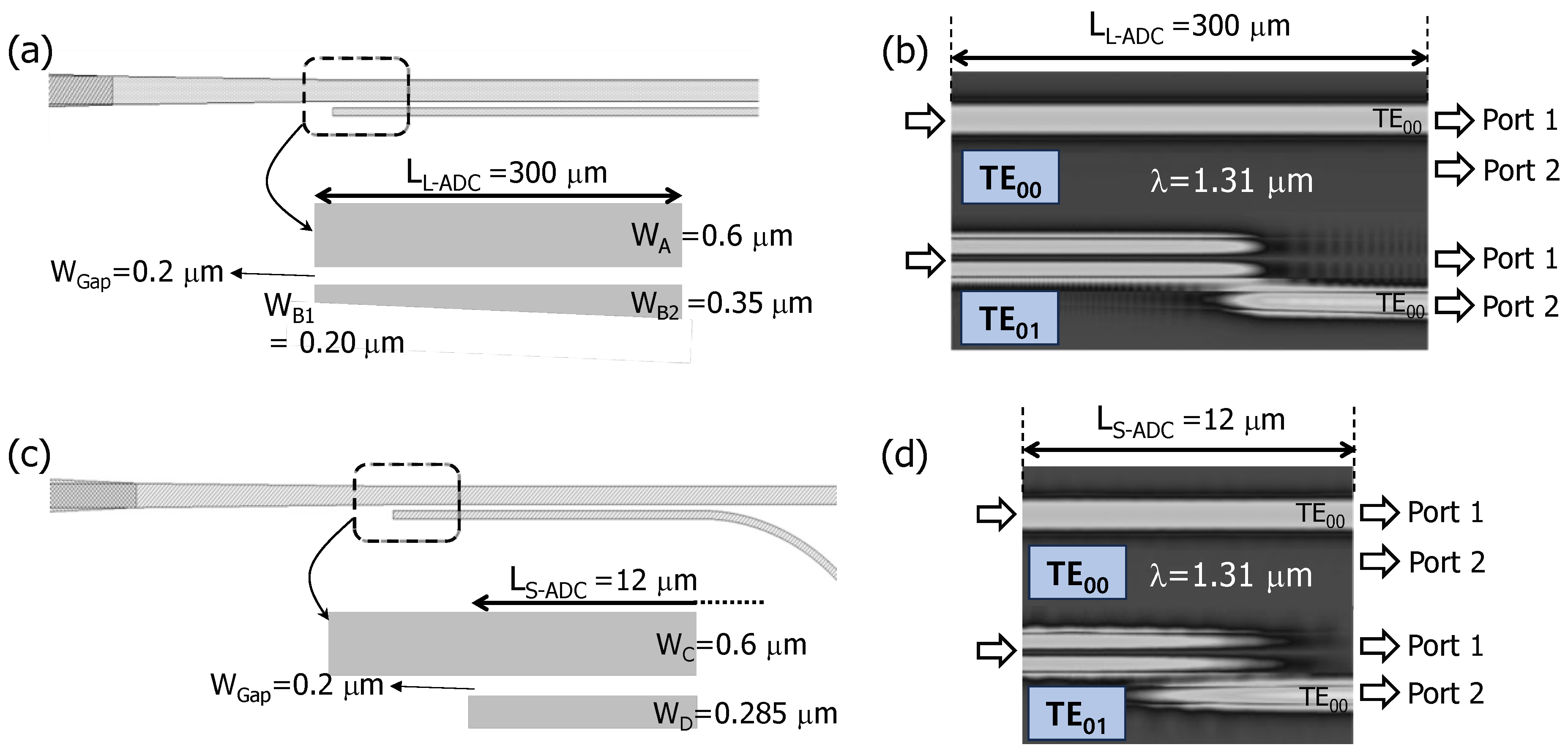
In this investigation, we devised, theoretically identified, and experimentally validated two varieties of ADC structures [
36].
Figure 3 shows the simulated propagation characteristics for the above-mentioned ADC-based mode split areas: (a) the long-length ADC (L-ADC)-based mode split area and the structure parameters for the taper-type L-ADC, (b) the propagating mode profile along the full L-ADC region (λ
in = 1.31 μm), (c) the short-length ADC (S-ADC)-based mode split area, and (d) the propagating mode profile along the full S-ADC region (λ
in = 1.31 μm). A packaged software based on a three-dimensional beam propagation method (3D-BPM, BeamPROP
TM; Synopsys, CA, USA) was utilized for the numerical analyses shown in
Figure 3b,d. For the L-ADC scenario, the W
Gap value was selected to make fabrication easier in the currently used foundry process, whereas the W
A, W
B1, and W
B2 values were adjusted to enable TE
01-mode transferring to neighboring waveguides. Conversely, for the S-ADC scenario, the W
C and W
D values were fine-tuned to ensure efficient perfect mode coupling for the specified W
Gap condition.
Achieving TE
00-mode coupling to an adjacent nanowire poses challenges because of the notable index mismatching between the two coupled nanowires in the ADC configuration. However, in two scenarios depicted in
Figure 3 (L-ADC and S-ADC), the optimization of the narrower waveguide width makes index matching easier between the TE
00-mode and TE
01-mode. This enables the TE
01-mode, converted from the TM
00-mode, to be interacted to the counterpart output channel as TE
00-mode. Consequently, arbitrarily polarized input signals can be transferred as TE
00-mode output port in the PSR (
Figure 3b,d).
The L-ADC depicted in
Figure 3b employs a linear tapering technique within a narrower nanowire side, which enables different wavelength components to achieve similar index matching by gradually widening the waveguide from W
B1 to W
B2 along the L
L-ADC, spanning 300 μm. As a result, the operational wavelength range of the PSR could be expanded. Put simply, the L-ADC scheme demonstrates greater resilience to variations in coupled waveguide parameters stemming from fabrication imperfections. As illustrated in
Figure 3b, when utilizing the parameters outlined in
Figure 3a, only TE
01-mode transfers to couple to the neighboring nanowire, while TE
00-mode traverses the ADC region without undergoing any interaction on mode coupling.
The S-ADC depicted in
Figure 3c adopts a structure without any tapering. By optimizing parameters such as the W
C, W
D, and W
Gap of the coupled waveguides for a particular wavelength (λ = 1.31 μm), the coupling length (L
S-ADC) can be decreased to 12 μm, which is shorter than that of the L-ADC by a factor of 25. One possible shortcoming of the S-ADC scheme, however, is its slightly lower allowance for fabrication errors. In this study, the ADC design was carefully selected based on the fabrication precision required for both the PSR and the optical DeMUXs (i.e., S-ADC in the PSR for the 100-GHz-spaced 16λ DWDM optical DeMUX, and L-ADC in the PSR for the 20-nm-spaced 4λ CWDM optical DeMUX).
Currently, mode split areas based on the L-ADC and the S-ADC have a trade-off relation between a small footprint and operating wavelength range. Meanwhile, recently, by adopting a metamaterial scheme engineered by means of structural anisotropy or a slot waveguide structure, an extremely small footprint and wide operating wavelength window for silicon-nanowire-based polarization-handling components, such as polarization beam splitters, have been actively reported [
56,
57,
58,
59]. Incorporating such anisotropic configuration into the mode conversion and mode split areas could further enhance the performance of the PSR from the viewpoint of device footprint, operating wavelength range, and fabrication tolerance.
3. 100-GHz-Spaced 16λ DWDM Optical DeMUX
Previous studies have noted that DI-based optical DeMUXs offer technical benefits, including a compact footprint, minimal IL, low spectral crosstalk, and a flat-topped spectral response [
20,
21,
22,
23,
24,
25,
26,
27,
28,
29,
30,
31,
32,
33,
34,
35,
36]. However, these advantages tend to diminish when the channel count exceeds 8 and the channel spacing narrows below 400 GHz, especially when the optical demultiplexing function is achieved passively rather than through external active control [
15].
In our earlier studies, several types of silicon-nanowire-based optical DeMUXs utilizing cascade-connected multiple DIs [
22,
23,
24] and arrayed waveguide gratings (AWGs) [
41,
42] were reported. To enhance the WDM transmission capability further, increasing the channel count (N
Ch) of DeMUX is necessary. Typically, augmenting N
Ch in AWGs is straightforward. However, as N
Ch increases, IL and filter spectral uniformity tend to degrade [
43,
44]. While enhancing the free-spectral range (FSR) of the AWG could be one of solutions to improve IL and spectral uniformity, it might significantly enlarge the footprint to maintain filter specifications such as bandwidth and spectral noises [
43].
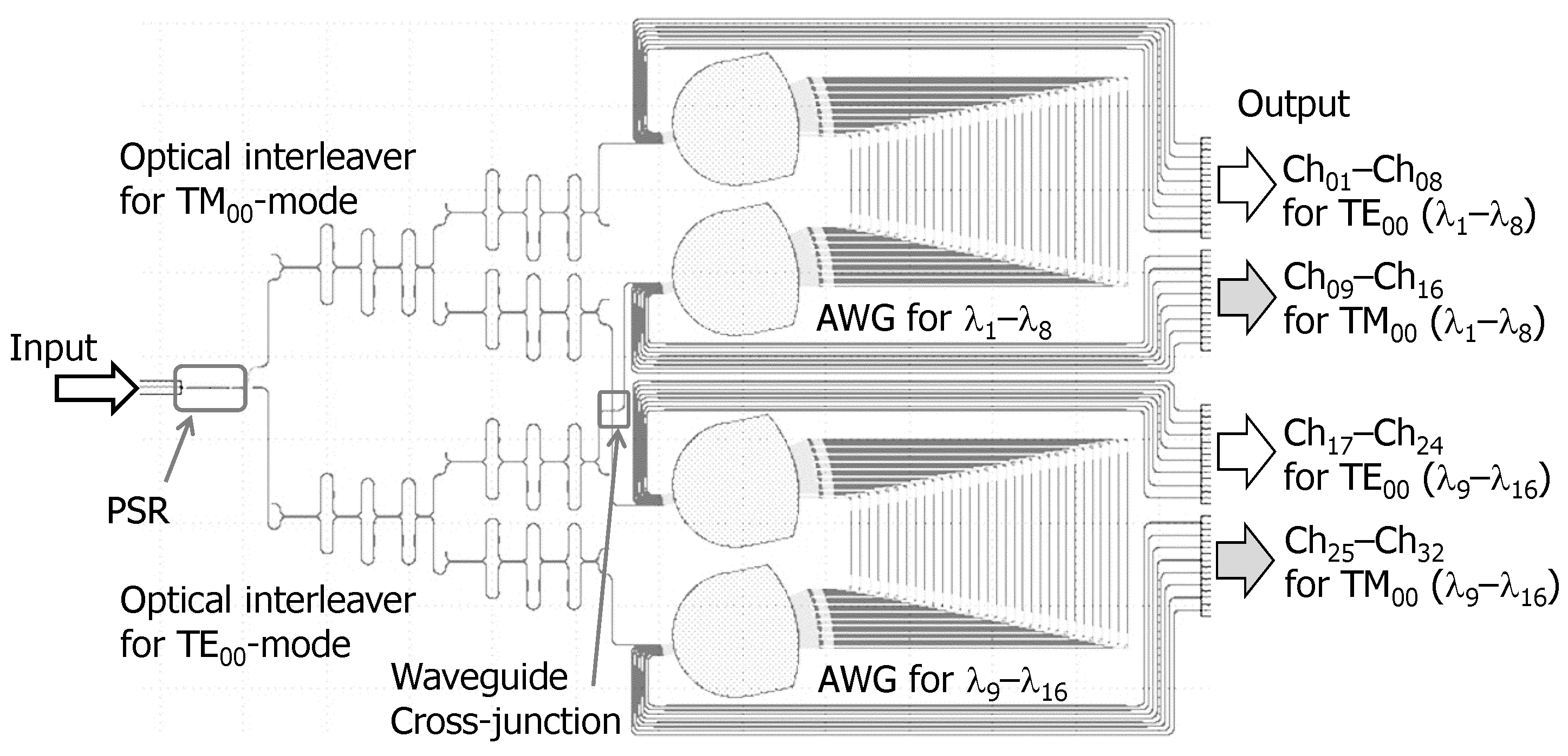
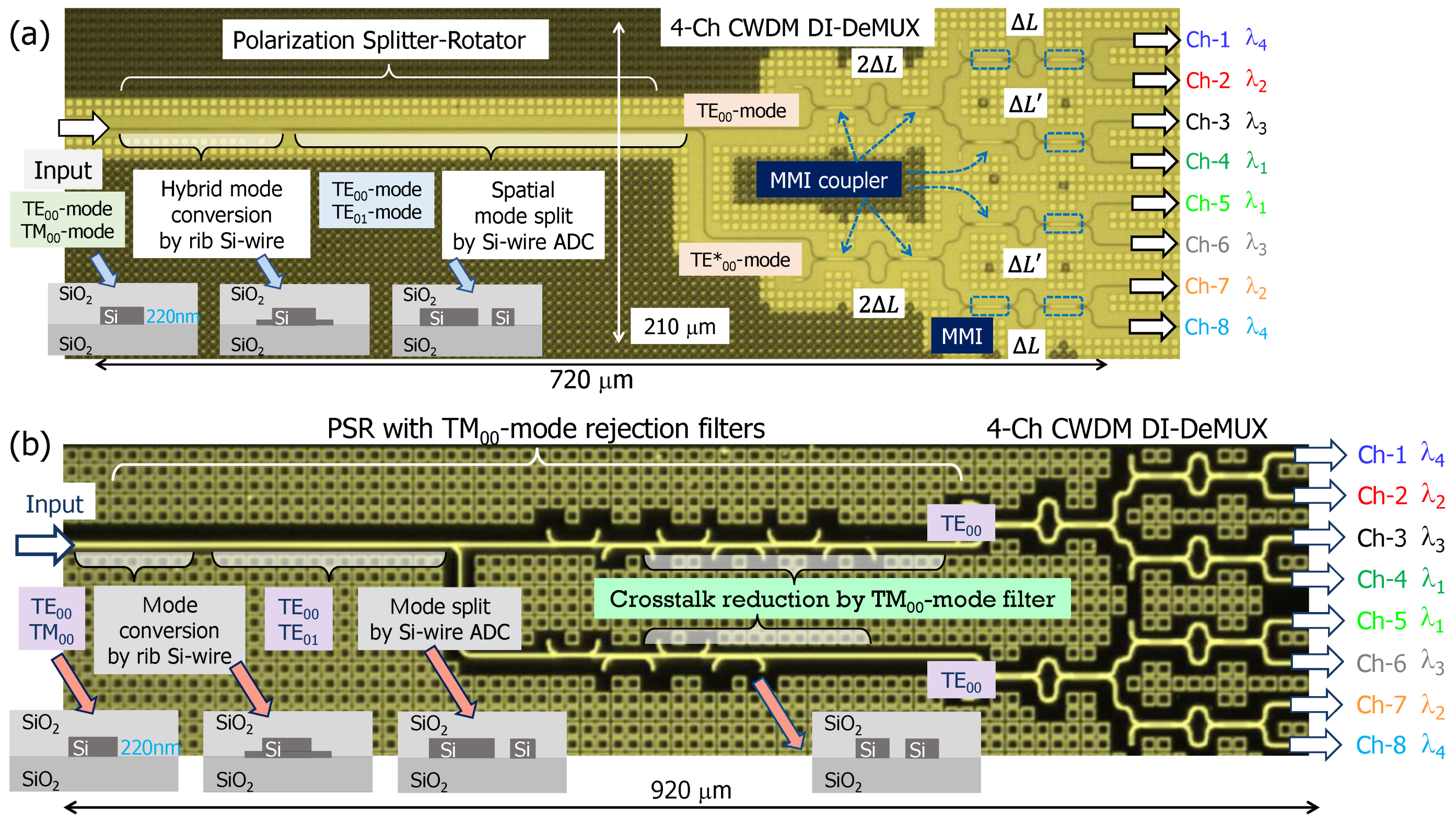
Introducing another way to address the aforementioned issue, we devised a novel DeMUX configuration comprising box-like spectral DI-type optical interleavers and pairs of AWGs. Through the incorporation of an 8λ-AWG and a flat-topped interleaver, we effectively discriminate between two 8λ spectral bands separated by the FSR of the AWG. This allows us to double the channel expandability of the optical DeMUX to 16λ without compromising on IL and channel uniformity. The schematic of the polarization-diversified 16λ optical DeMUX [
49] is shown in
Figure 4. For polarization diversity, the PSR discussed in
Section 2 was integrated into the optical DeMUXs. The configuration includes the identical DI-type flat-topped optical interleavers and the identical counter-propagating-type 8λ-AWGs, which gives a total output channel number of 32, as indicated in
Figure 4.
Randomly polarized signals are processed into the spatially separated ports with TE
00-mode. Subsequently, each TE
00-mode light undergoes processing using identical wavelength filters. In order to ensure the precise alignment of the filtering peaks between the two different polarization inputs, we devised both optical signals to be handled by the counter-propagating type 8λ-AWG whose light paths are the same, which guarantees minimal polarization-sensitive wavelength shift [
42]. Notably, the device inherently incorporates a cross-junction to enable a compact polarization-diversified configuration. The crossover shape was designed to minimize the size of crossover, excessive loss (<0.1 dB), and leakage at the crossover (<−30 dB) [
23].
Since the 16λ optical DeMUX requires phase accuracy caused by relatively long interaction lengths, as seen in
Figure 5, ArF-immersion lithography technology featuring CMOS 40 nm node was adopted to fabricate the devices on a 300 mm SOI (silicon-on-insulator) waferscale with a 200-nm-thick silicon core layer and a 2-μm-thick BOX (buried oxide) layer [
53,
54].
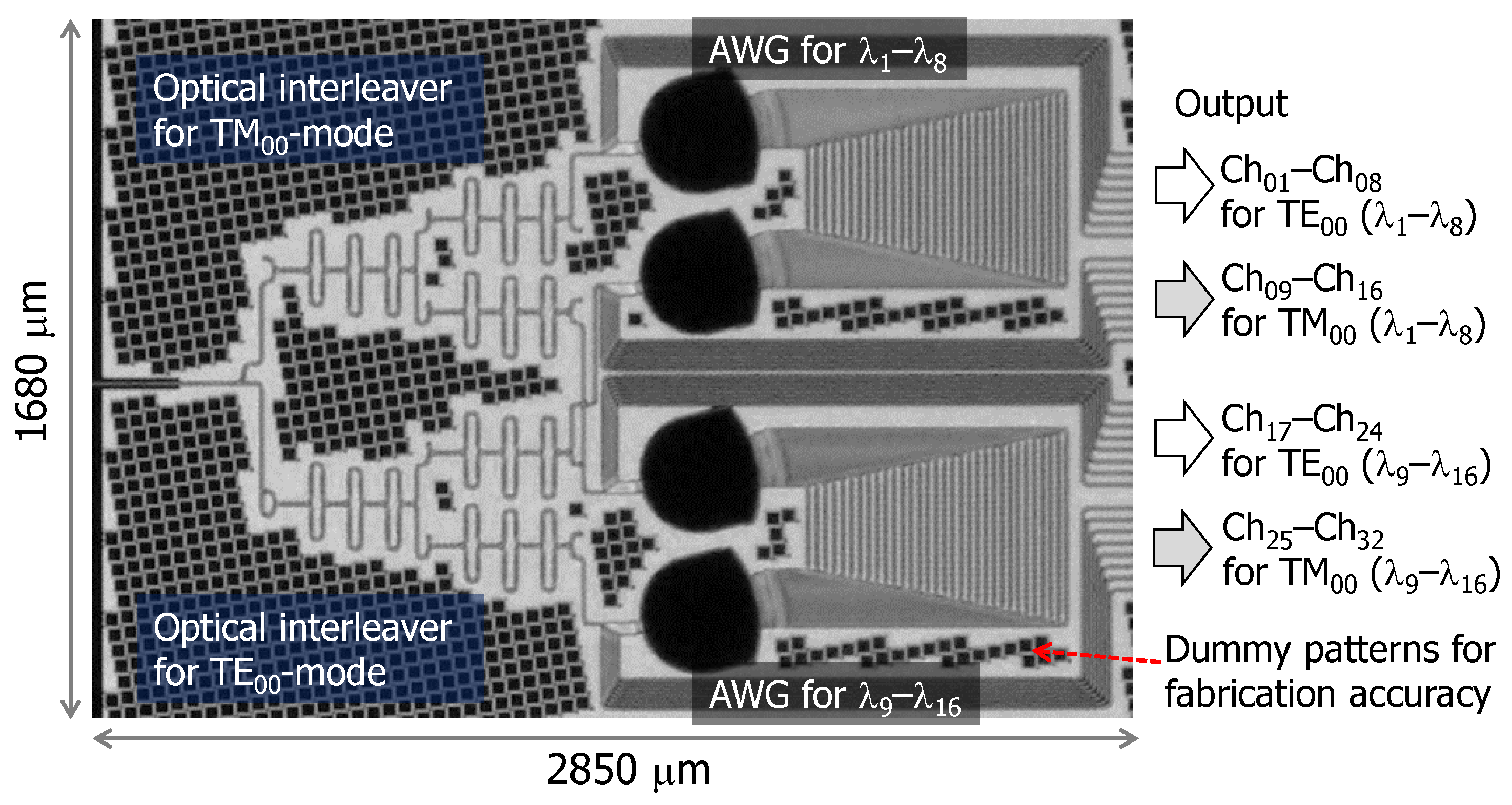
Figure 5 illustrates the fabricated polarization-diversified silicon-nanowire-based 16λ optical DeMUX, maintaining the entire structure shown in
Figure 4. The footprint was calibrated at 1.68 mm in width and 2.85 mm in length, encompassing the PSR, the two DI-type optical interleavers, and the 8λ-AWGs with a waveguide crossover. The S-ADC scheme was employed in the PSR for mode splitting, as the highly accurate ArF-immersion lithography process compensates for a relatively smaller fabrication tolerance for the S-ADC structure. Also, dummy tiles were used for fabrication accuracy.
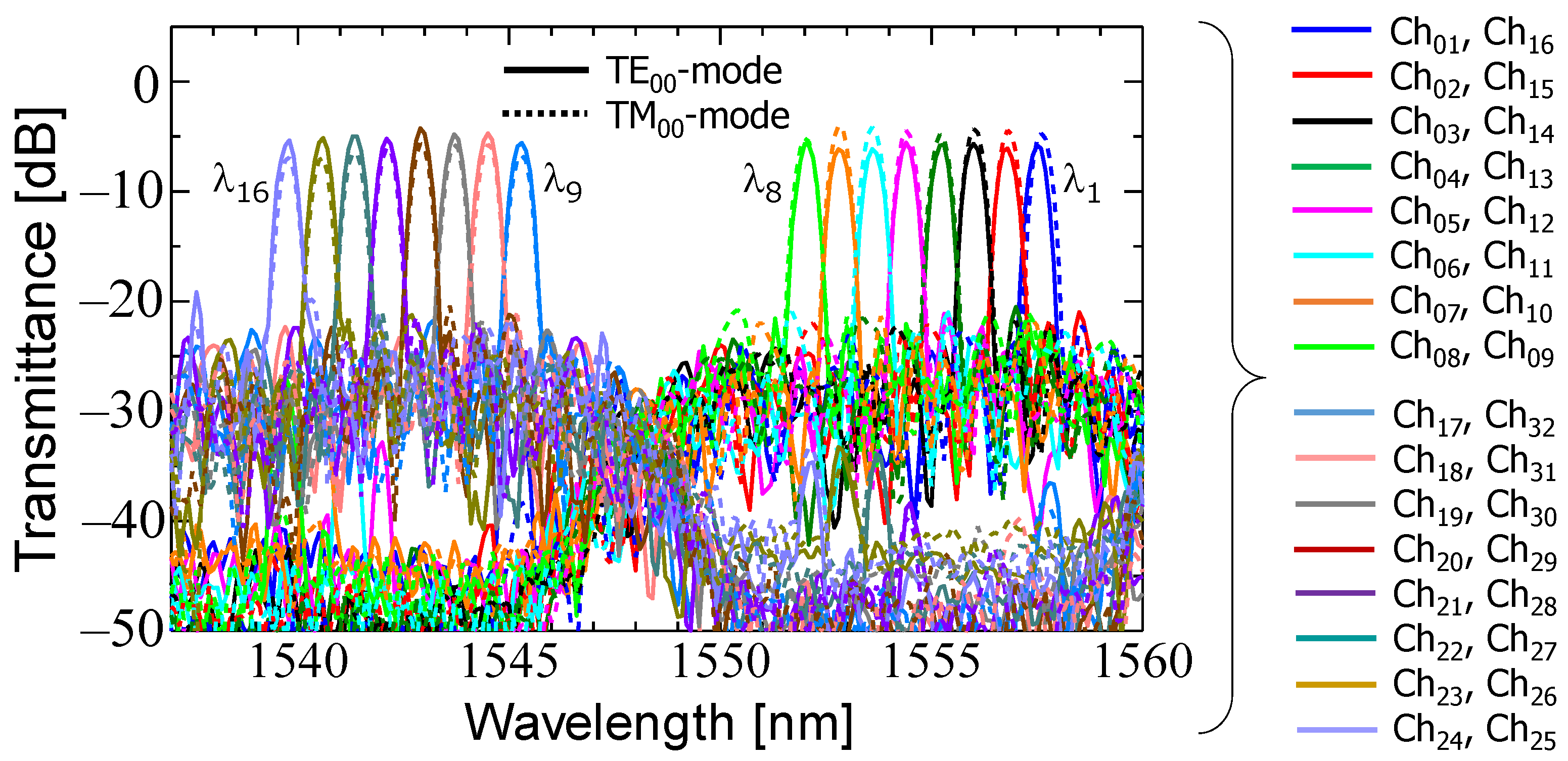
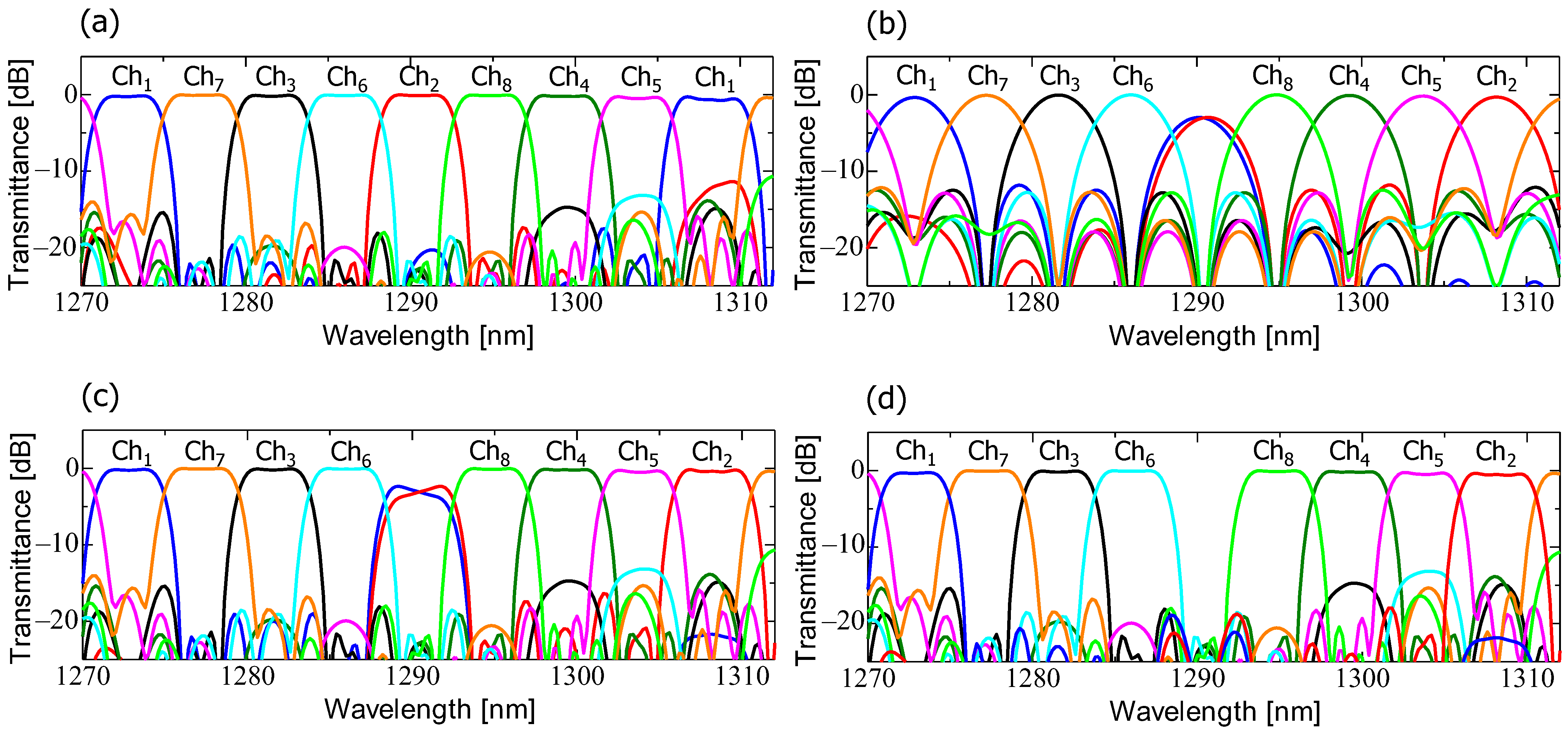
Figure 6 displays the spectral characteristics obtained from measurements, with solid and broken lines representing the transmittances for TE
00 and TM
00 mode input, respectively. It is worth noting that the transmittance depicted in
Figure 6 indicates the transmittivity subtracted by that of a bending-shaped single-mode waveguide for both polarization inputs. In other words, the transmittivity in
Figure 6 accounts for the excessive loss resulting from various filter architectures such as the PSR, the DI-based interleavers, and the AWGs. Given that the propagation loss of the waveguide is <0.5 dB/cm through the fabrication process [
54], the IL can be regarded as the excessive loss of the device.
For all output channels, the estimated peak transmittance ranged from −5 to −6 dB. It is noted that the transmittance shown in
Figure 5 was estimated by subtracting the coupling loss of 2.5 dB/facet between lensed single-mode fibers and the two narrow-tapered spot-size conversion areas of the fabricated device. Consistent with findings from our previous studies [
22,
54], we attribute the entire excess loss to 0.5 dB from the PSR, 0.5 dB from the DI-based interleaver, and 4.5 dB from the AWG. Notably, optimization efforts, as detailed in our prior work [
41], can potentially reduce the excess loss of the AWG to 1.2 dB. Experimental validation confirmed clear demultiplexing response for both linearly polarized lights. The measurement of 8λ spectra for both AWGs showed almost 0.8-nm-spaced (100-GHz). In
Figure 6, the interleaver effectively suppressed one of periodic 8λ spectral groups spaced by the FSR of the AWGs, by more than 25 dB.
This facilitated the distinction of all 16 wavelength signals, regardless of the input signal’s polarizations. However, a deviation of +5 nm from the simulation results was observed in the center wavelength (1555 nm) of the filter spectral group for λ
1–λ
8 (Ch
01–Ch
16) due to fabrication imperfections, necessitating adjustment through the optimization of fabrication processes or the control of design parameters. Notably, the filtering grids for each polarization were nearly the same of <0.1 nm owing to the shared lightwave paths facilitated by counter-propagation-type AWGs [
42]. Furthermore, the two separate AWGs demonstrated nearly the same 8λ spectral responses including the AWG’s FSR, reflecting the precision achievable with 300 mm waferscale ArF-immersion lithography [
54]. For all output channels, polarization-dependent loss (PDL) was evaluated to <0.5 dB.
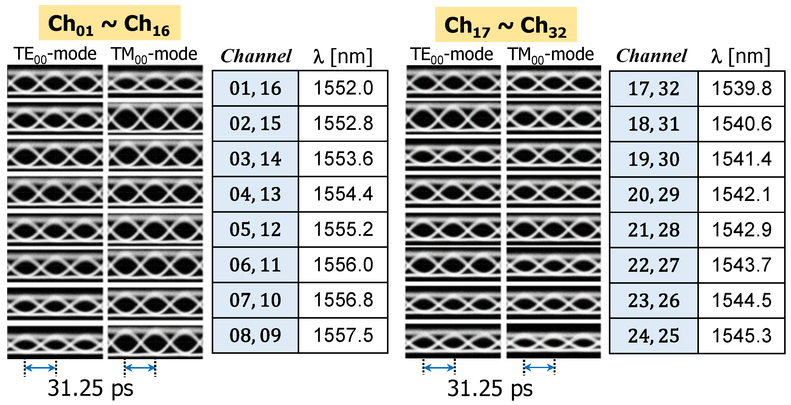
We also verified device functionality by implementing 32 Gbps NRZ (non-return to zero) WDM signal transmissions through the fabricated chip.
Figure 7 displays the calibrated eye patterns for the 32 Gbps NRZ signals (PRBS 2
31–1) with TE
00- and TM
00-mode inputs at all output channels. An optical source was provided by a tunable single-mode diode laser, and the NRZ modulated signal was generated using a commercial optical modulator. We controlled the input signal’s polarization properly. Subsequently, we launched each signal into the device through a polarization maintaining fiber. The output signal was detected using an optical oscilloscope.
As depicted in
Figure 7, we verified the functionality of the optical DeMUX by transmitting 32 Gbps NRZ modulated signals through it. We were able to confirm the clear opening of the eye diagrams at all output channels regardless of the input polarization states. It is important to note that the data rate was constrained solely by local experimental equipment. In the fabricated device, 3 dB filtering spectral widths for all outputs, as depicted in
Figure 6, were evaluated to be >0.42 nm, indicating the processing capability of the device up to >50 GHz of modulation bandwidth. In fact, we also observed clear eye openings for 50 Gbps NRZ modulated signals in similar transmission experiments.
As outlined in Ref. [
49], the 16λ optical DeMUX is a fully passive device, with its properties dictated by the phase relation of spatial light interferences across several optical paths within numerous DIs and AWGs. Consequently, the filter’s spectral response, including center wavelength and spectral crosstalk, is greatly affected by the fabrication technology. Given the high phase accuracy provided by the adopted 300 mm SOI waferscale ArF-immersion lithography process along the interaction lengths within DIs and AWGs, the static and dynamic spectral characteristics depicted in
Figure 6 and
Figure 7 remained consistent across the SOI wafer.
Meanwhile, the functionality of the 16λ optical DeMUX operation was not confined to the C-band spectral regime. Similar spectral characteristics were also experimentally verified in the O-band region. To adapt the device for O-band operation while maintaining single-mode conditions and considering chromatic dispersions between the DI-type interleaver and the AWG, adjustments were made only to the waveguide widths within each DI on the same SOI wafer used for the C-band option. Further details are available in Ref. [
49].
Table 1 provides a comparative analysis of various DWDM-like multi-channel optical DeMUXs. In contrast to single-filtering type devices documented in [
19,
44], the depicted device in
Figure 5 demonstrates reduced IL, increased channel count, and decreased spectral crosstalk. Furthermore, there was no report of polarization handling required in the receiver end for the combination-type devices [
45,
46], where an additional DI-based component interleaves AWG’s filtering spectra into even and odd wavelength parts. Only the proposed device scheme features polarization handling based on polarization diversity. When compared to silicon-nanowire-based devices, the proposed solution exhibits superior properties in terms of excess loss despite narrow channel spacing. Moreover, compared to a microring resonator-type device, the proposed scheme holds the possibility of additional channel count expansion. By adopting a 1×N (N: integer) type flatband DI-based interleaver [
21,
22] with a 1×M (M: integer) AWG, the total channel count could be scaled to N × M.
4. 800-GHz-Spaced 8λ LR-8 Optical DeMUX
Among the various data transmission specifications within short-reach interconnect datacenters, the 400GBASE-LR8 has emerged as a prominent standardization technology for 10 km reach employing SMFs, garnering active investigation [
33,
34,
38,
60,
61]. In the context of LR-8 targeted WDM interconnects, each operational grid is discretely delineated in the O-band region [
33,
38]. A silica-based flatband AWG-type optical filter has been reported as an optical DeMUX for LR-8 optical interconnect applications [
38]. In this setup, the discrete output channel relation was achieved by asymmetrically positioning the output waveguide arrays in the second half of the slab area. However, a number of challenges persisted. The AWG typically has a large device size and inherently large IL caused by the optical spill over at the slab areas. Additionally, achieving flatband spectral response necessitated the use of multimode access waveguides in the slab region. Consequently, it is extremely difficult to employ the device architecture on the transmitter side. Moreover, a silica-based material flatform is not appropriate for integrating with other silicon-based active components such as optical modulators and photodetectors.
Thus far, efforts have been made to address the aforementioned limitations by introducing a silicon-nanowire-based optical DeMUX employing cascade-connected DIs [
33]. Here, although the discrete LR-8 spectral relation was attained by controlling a certain optical path difference at the third-stage DI, the suppression rate of unwanted spectral components at around λ = 1291 nm was as high as −4 dB. In addition, the spectral response exhibited a Gaussian-function shape, which may not be suitable for practical applications.
To address lingering technical challenges, we introduced and theoretically validated a non-Gaussian box-like spectral-optical DeMUX scheme intended for LR-8 400GbE datacenter applications [
34].
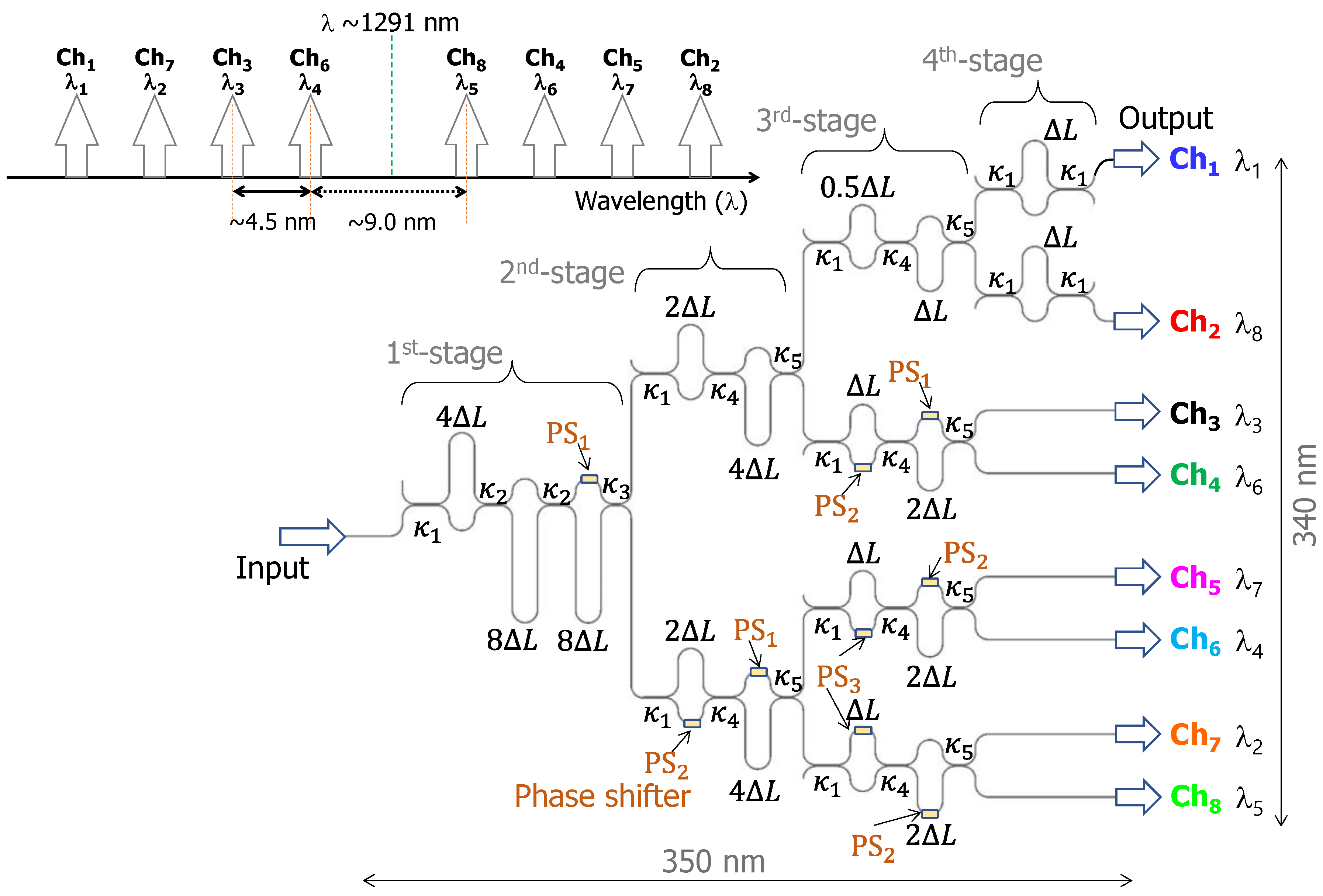
Figure 8 illustrates the schematic diagram of the LR-8 targeted optical DeMUX, along with the specified operating grids and the position of the required phase shift within each DI [PS
1 =1.0π (rad.), PS
2 =0.5π (rad.), PS
3 =0.25π (rad.)]. The device needs four-stage multiple DIs. While eight wavelengths can be spatially filtered out without the fourth-stage DI [
21], adherence to conventional design guidelines [
21,
22] did not align the operating wavelength grid with the LR-8 grid due to the cyclic spectral nature of multi-stage DIs. In contrast, in a prior study [
33], the deliberate adjustment of one of the optical path differences at the third-stage DI to half compared to others aimed at breaking the aforementioned cyclic spectral nature, thus allowing alignment with each LR-8 grid. However, despite clear spectral differences around λ = 1291 nm, the spectral noises remained unacceptably high at approximately −4 dB. This prompted the adoption of the fourth-stage DI in the optical DeMUX configuration.
In this case, the fourth-stage DI serves to cut out the unwanted spectral range at around λ = 1291 nm, thus reducing spectral crosstalk to less than −20 dB. To achieve this filtering operation, the optical path differences for the third and fourth DIs of Ch-1 and Ch-2 were appropriately optimized to completely out of phase at around λ = 1291 nm. Meanwhile, remaining device parameters in the proposed device were adjusted to achieve a flatband spectral response, as described in prior works [
21,
22]. The first delayed Mach–Zehnder interferometer with integer multiple values (=4ΔL, 2ΔL, ΔL) at all DI stages defines all central filtering peaks. In addition, cascade-connected multiple interferometers at all DI stages create a box-like spectral shape, accomplished by properly adjusting coupling ratios at each DI stage (κ
1 = 0.5; κ
2 = 0.2; κ
3 = 0.04; κ
4 = 0.33; and κ
5 = 0.08) and each optical path difference. As depicted in
Figure 1, the silicon-nanowire-based proposed scheme implies a total chip size of 350 μm in length and 340 μm in width.
The LR-8 optical DeMUX scheme’s spectral response was modeled using the scattering matrix method and coupled mode theory [
21,
22,
23,
24]. The wavelength-sensitive coupling ratios of silicon-nanowire directional couplers (DCs) were formulated, and their spectral validity was corroborated by the previous data [
24]. As the waveguide structure, we designed 350-nm-wide and 220-nm-thick silicon-nanowire channel waveguides operating in the O-band region. The separation gap of each DC was uniformly designed as 0.2 μm, adhering to standard conditions in the currently available CMOS-based foundry process. Following these design guidelines, various DC splitting ratios were numerically simulated using the 3D-BPM method (BeamPROP
TM; Synopsys, CA, USA). Subsequently, their outcomes were integrated into the main loop of the scattering matrix for the multiple DI-type optical DeMUX.
Figure 9 illustrates the computed spectral properties of LR-8 channels: (a) a conventional box-like spectral optical DeMUX based on multiple DIs [
21], (b) a Gaussian-shaped DI-based DEMUX achieved through local path difference control at the third-stage DI [
33], (c) the design combination described in Refs. [
21,
33], and (d) the proposed DI-based optical DeMUX incorporating extra band elimination filters [
34]. It is noted that the path differences for each DeMUX were commonly set to maintain an inter-channel gap of 800 GHz.
In
Figure 9a, achieving flatband involves cascade-connecting excessive interferometers at each DI stages. The operating window is inclined to show an equidistant spacing of 800 GHz, resulting in a difficulty in discriminating LR-8 optical signals. In
Figure 9b, the proper control of the path difference at the third-stage DI inhibits the unwanted band at approximately λ = 1291 nm [
33]. However, the extinction ratio (ER) is not small enough to maintain a sufficiently low WDM system penalty.
Figure 9c demonstrates that combining the design strategies from
Figure 9a,b provides spectral distinction with a box-like spectral response. Nevertheless, it is noted that an inadequate ER of <4 dB still remains.
Figure 9d shows that the proposed LR-8 DeMUX dramatically relaxes the drawback on ER to >20 dB without compromising the quality of the flatband spectral response. Further enhancements such as reducing the wavelength dependence of DC coupling efficiency or incorporating multimode interference (MMI) couplers would make the proposed LR-8 DeMUX more practical in applications.
Table 2 provides a comparative analysis of various LR-8 targeted optical DeMUXs. In contrast to previously reported devices documented in [
33,
38], the proposed device illustrated in
Figure 8 offers numerous advantages in terms of small footprint, low IL, spectral crosstalk at around λ = 1291 nm, spectral flatness, and other factors. Compared to silicon-nanowire-based devices, the proposed scheme exhibits superior spectral qualities, albeit requiring experimental verification. Needless to say, integration with the PSR alongside the LR-8 optical DeMUXs enables the detection of arbitrarily polarized LR-8 optical signals based on polarization diversity, as experimentally evidenced in
Figure 6 and
Figure 7.
5. 20-nm-Spaced 4λ CWDM Optical DeMUX
CWDM provides many advantages over DWDM due to its less strict prerequisites for the accurate control of diode laser oscillation frequency and broader available operating range in the wavelength domain. Additionally, CWDM devices must properly work within a wavelength range exceeding 60 nm, as the operating point is spaced by 20 nm [
5,
6,
7,
11]. Furthermore, the optical DeMUX at the receiver’s end must possess the capability to handle arbitrary polarization input signals [
28,
30,
35,
36,
40,
42,
47,
49]. To date, various methods have been investigated to manage randomly polarized CWDM signals for use in the optical receiver, which can be categorized into three groups: the zero-birefringence scheme [
28], the polarization compensation scheme [
30,
40], or the polarization diversity schemes [
35,
36,
47,
49], applied to silicon nitride (SiN) [
28,
40,
47] and silicon (Si) [
30,
35,
36,
49] materials.
The zero-birefringence scheme finds extensive application within SiN material systems [
28], employing square-like core shapes to eliminate wavelength sensitivities of the split/coupling response and achieve nearly identical equivalent index in optical waveguides. Despite experimental validations of the zero-birefringence in the SiN waveguides, there still remains nonnegligible spectral discrepancy between the TE
00 and TM
00 modes. SiN-based AWG based on polarization-compensation has also been deployed for use in CWDM systems [
40], enabling operation regardless of the input polarizations through lateral asymmetric-core-shaped polarization rotators within each arrayed waveguide of the AWG. Nonetheless, additional study is required to overcome drawbacks such as large device size, relatively small fabrication margin for polarization rotators, and the complexity of monolithic integration to silicon-nanowire-based components.
Additionally, a silicon-nanowire-type CWDM DeMUX was reported [
30], due mainly to its compactness and feasibility of monolithic integration. The polarization issue associated with silicon-nanowire waveguides has been addressed through the implementation of the polarization compensation scheme. In this scenario, lateral asymmetric waveguide-based polarization rotators were located in the middle of all single-stage DIs. These components rotate the polarization by 90 degrees whenever the signal traverses each DI, facilitating the depolarization of the spectral response for all input polarizations. Achieving this involves utilizing a 340 nm thick silicon core layer to depolarize the optical split and coupling behavior of the bending-type DC. However, a thick core (beyond the standard value of 220 nm) may lead to technical difficulty in making the nanowire’s propagation loss lower. Moreover, the polarization rotators necessitate extreme precision in the lithography process such as electron beam lithography, rendering them unattractive for good productivity.
Overall, as mentioned earlier, in terms of polarization-handling CWDM DeMUXs, SiN-based devices exhibited issues such as spectral non-uniformity [
28], substantial footprint exceeding millimeter-scale lengths, and intricate fabrication processes [
40], along with challenges in integrating monolithically with silicon-nanowire-based devices [
62]. On the other hand, concerns regarding higher excess loss for propagation and increased manufacture precision due to a thicker core were raised for silicon-nanowire-based devices [
30]. Consequently, there have been few publications on silicon-nanowire-based polarization-handling CWDM DeMUXs.
Figure 10 depicts the fabricated polarization-diversified CWDM optical DeMUXs: (a) lacking TM
00-mode rejection filters and (b) incorporating TM
00-mode rejection filters. These devices typically incorporate a PSR to introduce polarization diversity, along with two DI-type optical DeMUXs of identical design for CWDM optical signal filtering. The design principles and operational concept of the PSR mirror those shown in
Figure 1. In instances where a mode split area relies on a rectangle-shaped silicon-nanowire ADC, a relatively narrower waveguide is linearly tapered, as depicted in
Figure 3b. Consequently, incident WDM signals with varied linear polarization states, such as combinations of TE
00-mode and TM
00-mode, are divided into the TE
00-mode signals and directed to spatially separated output channels of the ADC [
35].
The DI-based optical DeMUX is composed of three optical delaylines, each with adjusted path differences to achieve constructive interference at each CWDM grid, along with two identical 50:50 MMI couplers. It is crucial to emphasize that the optical DeMUX must span a wavelength range exceeding 60 nm. Therefore, MMI couplers were chosen over DCs, which exhibit sinusoidal coupling behaviors, to serve as optical couplers in each DI. The width of the silicon-nanowire waveguide in each DI, excluding the MMI region, was designed to be WCH = 350 nm.
The fabrication of the CWDM optical DeMUXs involved utilizing the ArF-dry lithography process on a 200 mm SOI wafer featuring a 220-nm-thick silicon core layer and a 2-μm-thick BOX layer. The mode split region in the PSR employed the L-ADC, considering the possible phase accuracy from the foundry process and the limitations of the feasible photomask design. To assess the filter spectral response, a tunable laser served as the optical source. The transmittance of the manufactured devices was calibrated using an optical vector analyzer (OVA) (OVA 5013; LUNA Innovations, VA, USA. Analyzing the Jones matrix of the output transmitted signals enabled the examination of the transmittance response from arbitrarily linear-polarized inputs to each type of output via SMFs [
63,
64].
In the measurement of the single-mode fiber-based optical transmittance of the fabricated devices, the temperature of the device was controlled to 25 degrees Celsius. It has been well known that, compared with the case for silicon dioxide, the refractive index change for single-crystalline silicon is much more sensitive to external temperature variation by a factor of 10 [
65,
66,
67,
68]. Since silicon has a relatively large thermo-optic coefficient of 1.8 × 10
−4 [1/K] [
65], the filter spectral peak for various kinds of optical DeMUXs tends to shift to the longer wavelength side by up to 0.07 [nm/K] as the temperature increases. Since the 4λ 20-nm-spaced DeMUXs have a relatively wider operating wavelength range, the temperature variation of 50 degrees Celsius (plus or minus 25 degrees Celsius) can be tolerable without any significant spectral penalties in terms of IL and spectral crosstalk. Meanwhile, the temperature-sensitive nature of silicon stimulated extensive work on energy-efficient thermal tuning by forming micro heaters on the silicon-nanowire waveguides [
69,
70,
71].
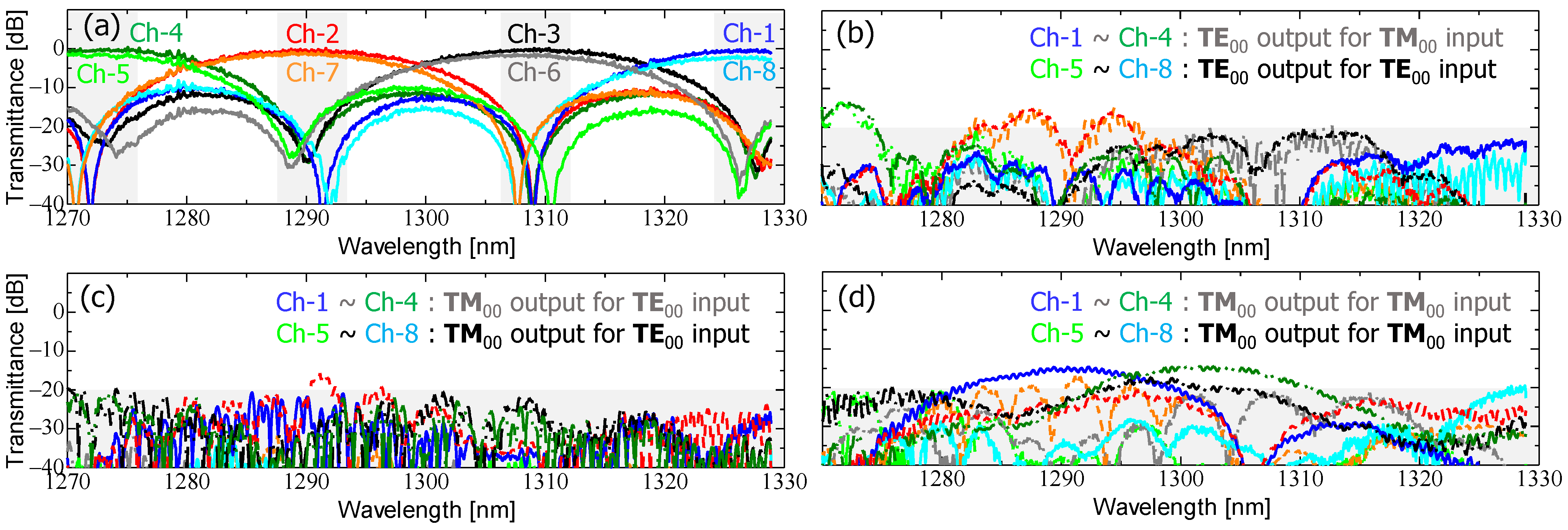
Initially, we assessed the transmission spectra of the fabricated device depicted in
Figure 10a. The spectra for all outputs spanning Ch-1 to Ch-8 are illustrated in
Figure 11. The following spectra shown in
Figure 11a–d were provided by the OVA: (a) main signals (TE
00-mode input to TE
00-mode output for Ch-1–Ch-4, TM
00-mode input to TE
00-mode output for Ch-5–Ch-8), (b) cross-coupled spectral noises (TM
00-mode input to TE
00-mode output for Ch-1–Ch-4, TE
00-mode input to TE
00-mode output for Ch-5–Ch-8), (c) TE
00-to-TM
00-mode polarization spectral noises (TE
00-mode input to TM
00-mode output for all outputs), and (d) TM
00-to-TM
00-mode polarization spectral noises (TM
00-mode input to TM
00-mode output for all outputs).
As seen in
Figure 11a, we were able to experimentally validate CWDM demultiplexing spectra whose output responses are nearly depolarized. All outputs displayed
sinc-function-shaped nearly ideal response, spaced by 20 nm, indicating the spatial separation of the TE
00-mode input from the upper output of the PSR without undergoing any hybrid mode change, and directed into the upper-sided DeMUX. Conversely, TM
00-mode inputs were confirmed at outputs from Ch-5 to Ch-8. In spite of the pronounced structural birefringence of the silicon-nanowire waveguide, we clearly observed closely resembling spectra, which specifies that only the TM
00-mode components experienced hybrid mode change to TE
01-mode, with its propagation mode then being split as the TE
00-mode in the L-ADC. As a result, random polarized signals were effectively discriminated within the 60-nm-wide spectral window, showcasing an excessive loss of <1.0 dB and a PDL of <1.0 dB. That is, excessive loss indicates the extra loss incurred compared to the propagation loss of bending-shaped nanowires with the same length, accounting for losses stemming from hybrid mode change, spatial mode split, and MMI interactions. Spectral noises coming from adjacent nanowires were evaluated at −20 dB for the peak transmittance of each four outputs.
The measured responses in
Figure 11b–d illustrate different forms of spectral noises. In a sense, these response levels should be thoroughly minimized because they are not necessary at all. Somewhat elevated residual polarization spectral noises observed in the PSR result from inadequate mode change in the shallow-edged waveguide region and an insufficient mode split efficiency in the L-ADC, especially concerning TM
00-to-TM
00-mode polarization spectral noises.
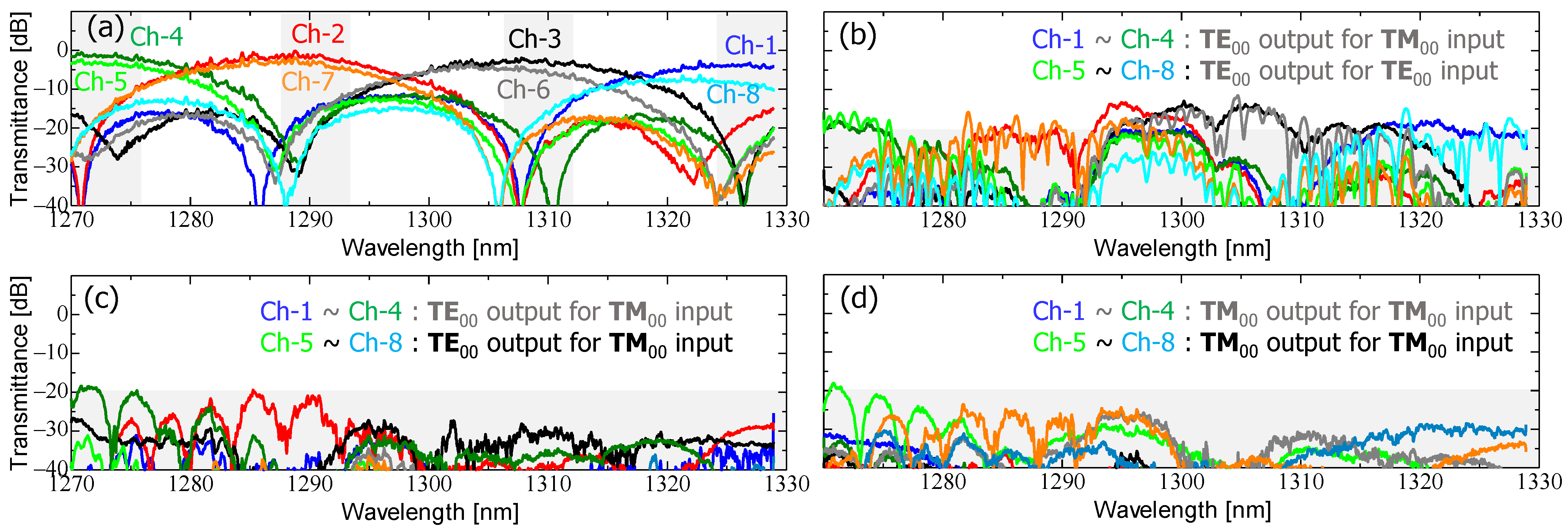
To make clear those concerns, TM
00-mode elimination cutters, utilizing a cascade-connection of symmetric DCs, were sequentially attached to the PSR. We tested the polarization-diversified optical DeMUX integrated with TM
00-mode elimination cutters (depicted in
Figure 10b). In
Figure 12a, it is evident that the primary signals were filtered out regardless of their polarizations. Moreover, the transmission of the cross-coupled spectral noises was blocked by <−20 dB across the entire O-band region, which is similar to the outcome seen in
Figure 11b. Additionally, measured spectra involving the integration of external filter arrays with the PSR (shown in
Figure 12c,d) exhibited a notable suppression of >20 dB in TM
00-mode-related polarization spectral noises compared to the data depicted in
Figure 12c,d.
It is noted that the spectral properties for the main signals and cross-coupled noises presented in
Figure 12a,b exhibit some degree of inferiority compared to those shown in
Figure 11a,b, particularly concerning excessive loss, spectral uniformity, and spectral noise level. This discrepancy is not attributable to the presence of TM
00-mode elimination cutters but rather stems from fabrication imperfections. These problems are most likely due to the shallow-etched nanowire structure, influenced by the double patterning process impacting hybrid mode change, and the channel waveguide shape, affected by dry etching processes impacting pattern width accuracy compared to the design and fabrication, as well as the magnitude of statistical random phase deviations at each DMZI, contingent upon line edge roughness. We believe that these fabrication imperfections are a temporary drawback. Once again, such double patterning structures can be managed by the commercially available silicon photonics foundry process [
55]. Considering more advanced lithography technologies as explained in Ref. [
54], we believe that the double patterning structures would be no obstacle for densely integrated high-performance circuits.
The devices depicted in
Figure 12a,b exhibited distinct spectra because they were manufactured on different SOI substrates at different points in time. As illustrated in
Figure 12a, the excess loss at each filtering wavelength slightly increased as the wavelength shifted towards the longer wavelength side. These phenomena could be attributed to fabrication errors, leading to the MMI width being narrower than intended in the photomask design. Consequently, a narrower MMI width caused the optimal split and coupling conditions to shift to the shorter wavelength side, occurring at approximately λ = 1.26 μm. On the other hand, the degraded spectral uniformity and relatively high PDL were associated with statistically increased random phase errors at each DI. We anticipate that the meticulous management of the fabrication procedure will resolve these shortcomings.
Lastly,
Table 3 provides a comparative analysis of various types of polarization-handling-based CWDM optical DeMUXs. Compared to previously reported studies [
28,
30,
40], the proposed optical DeMUX demonstrated spectral advantages regarding device footprint, IL, and polarization crosstalk. As mentioned earlier, it is worth noting that the reason for the inferior IL and PDL observed in the proposed device scheme integrated with TM
00-mode rejection filters was primarily due to fabrication imperfections rather than the integration of the TM
00-mode rejection filters. As indicated in
Table 3, a SiN-based optical DeMUX based on Echelle grating was also reported [
72]. Based on different propagation constants and diffraction conditions for TE
00-mode and TM
00-mode input signals in the Echelle grating region, the diffracted CWDM output signals were filtered out to spatially separated output channels. Among SiN-based optical DeMUXs, this one features a small footprint by utilizing the folded back interaction in the Echelle grating.
For satisfying the requirements of practical interconnect applications for integrated components, optical DeMUXs with a box-like response are highly desirable. This allows for simplified operation control for laser sources. In the case of the DI-based device scheme, achieving such a need involves connecting additional DIs with diverse coupling efficiencies and path differences to modify the scattering matrices of the DI-based interferometers [
21,
22,
28,
30].


