Abstract
In this study, a traveling wave Mach-Zehnder intensity modulator (TW-MZM) was designed and optimized for six different electro-optical (EO) crystals: lithium niobate (LNB), potassium niobate (KNB), lithium titanate (LTO), beta barium borate (BBO), cadmium telluride (CdTe), and indium phosphide (InP). The performance of each EO crystal, including optical and radio frequency (RF) loss, applied voltage, and modulation bandwidth, was estimated and compared. The results suggest that, in theory, KNB, LTO, BBO, and CdTe have the potential to outperform LNB. However, it should be noted that the loss associated with KNB and LTO is comparable to that of LNB. The findings demonstrated that BBO and CdTe exhibit a modulation bandwidth exceeding 100 GHz and demonstrate the lowest loss among the considered crystals based on the assumed geometry.
1. Introduction
A traveling wave Mach-Zehnder intensity modulator (TW-MZM) offers high-bandwidth modulation [1]. It operates based on the electro-optic (EO) effect, enabling light intensity modulation at the output by adjusting the applied voltage to control the imposed external electric field. This modulator consists of a Mach-Zehnder interferometer with two arms through which the light signal travels, and there is a modulator section integrated into one of the arms [2]. The modulator section is designed as a transmission line with periodically spaced electrodes, creating a radio frequency (RF) traveling wave electric field that interacts with an optical waveguide. The RF traveling wave electric field continuously interacts with the light signal along the transmission line, resulting in the efficient modulation of the light intensity. In contrast, other types of intensity modulators, such as the lumped-element Mach-Zehnder modulator (LE-MZM), have a limited interaction length, leading to lower modulation efficiency [3,4]. The distributed interaction with the optical waveguide yields a high bandwidth and enhances the frequency response of the device, making it suitable for ultra-high-speed optical communication systems [1]. The continuous interaction between the RF electric field and the light signal, along with the distributed nature of the modulation, minimizes nonlinear effects that can degrade signal quality. Therefore, this feature can benefit applications requiring high-fidelity transmission, such as coherent optical communication systems.
Bisht et al. (2010) [5] studied the anomalous spectral behavior of polychromatic light in a modified Mach–Zehnder (MMZ) Interferometer. They proposed two models using the MMZ interferometer for spectral switching-based information encoding and processing. Besten (2004) [6] investigated the integration of WDM-lasers based on an array of semiconductor optical amplifiers (SOAs), an arrayed waveguide grating (AWG), and RF modulators based on a TW-MZM.
The performance of a TW-MZM depends on the selected geometry, the EO medium, and other materials employed in other layers. This study aimed to investigate the effects of different EO materials on the performance of the TW-MZM after optimizing for velocity matching between the RF and optical waves in the case of using each of those six EO mediums. This approach to optimizing the TW-MZM and evaluating the achievable bandwidth and losses was first introduced by Pascher et al. in 2003 [7]. In that research, Pascher et al. (2003) [7] assumed a structure for a TW-MZM. They optimized that structure for using InP as the EO medium to match the phase velocity of the RF wave to the group velocity of the optical wave. They reported the loss and the potential modulation bandwidth of that TW-MZM using InP as the EO medium.
The type, structure, and materials should be considered when developing a model to design and simulate a light modulator. In other words, the modulator’s materials, type, and structure will be the model’s inputs. The model’s outputs will be the optimum geometry and operating parameters, such as the minimum applied voltage to modulate the light in a guiding mode, as well as the absorption, reflection, transmission, propagation constant, and the effective index associated with the fundamental mode. By analyzing the propagation modes of the RF wave, it is possible to adjust the silicon oxide thickness to match the velocity between the RF wave and optical wave and find the modulation bandwidth. That is because the thickness of SiO2 does not affect the propagation constant of the optical wave and can only control the velocity of the RF wave.
This study presents a comprehensive numerical model for designing and simulating a Mach-Zehnder intensity modulator with traveling wave electrodes. The model considers six different EO mediums: lithium niobate (LNB), potassium niobate (KNB), lithium titanate (LTO), beta barium borate (BBO), cadmium telluride (CdTe), and indium phosphide (InP). This investigation assumed and optimized a specific geometry for each EO crystal. The analysis involved estimating and comparing various parameters, including the required voltage, the optical and RF losses, the voltage length product, and the modulation bandwidth.
2. Materials and Methods
2.1. Selecting the Material and Geometry
Traditional nonlinear materials are generally classified into organic and inorganic categories. Inorganic nonlinear materials can be further categorized into dielectric materials, including LNB, BBO, and barium titanate (BTO), as well as Group III–V and Group II–VI semiconductors, such as InP, CdTe, and gallium arsenide (GaAs). Some of the traditional nonlinear materials and their main properties are listed in Table 1 [8].

Table 1.
The main properties of some traditional χ(2) materials.
In addition to traditional χ(2) materials, which typically exhibit relatively low nonlinearities, there are engineered quantum well heterostructures, such as JRD1 in polymethylmethacrylate, demonstrating nonlinearities that are 10–100 times greater than those of traditional χ(2) materials [9]. However, these specific, engineered, quantum well heterostructured materials were not considered in this study.
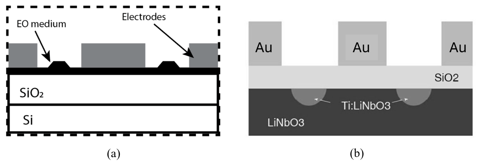
The optimum geometry of a MZM is varied by the selected material. For example, a model optimized for LNB is not optimized for other EO materials. No matter what geometry is selected, it must be optimized for the maximum transmission and minimum loss in the guiding mode. Figure 1 compares the geometry of a conventional MZM with that of the MZM used in the model developed in this study. Figure 2 shows the other geometries of the light modulators based on BTO, PZT, organic EO materials, and LNB, as presented by other researchers [9,10,11,12].
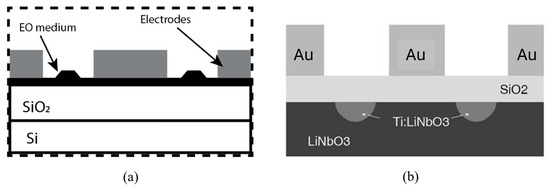
Figure 1.
The geometry of the MZM considered in this study (a) versus that of a conventional MZM (b).
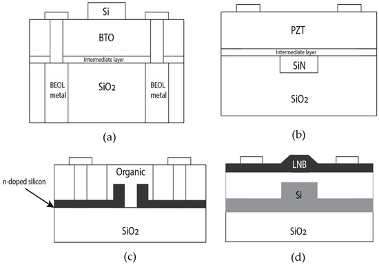
Figure 2.
The geometries of the light modulators based on (a) BTO, (b) PZT, (c) organic EO material, and (d) LNB.
2.2. Selecting the Type and Architecture of the Modulator
Generally, the traditional light modulator has a bandwidth of around 35 GHz. In contrast and in theory, integrated CMOS-compatible light modulators can have a bandwidth of greater than 100 GHz, and their voltage length parameter (V.l) is between 1 to 3 V·cm, depending on its type, geometry, material, and electrode type [13].
Optical modulators manipulate the output amplitude or phase of light waves as they pass through the device. Waveguide-based modulators are used in communication applications to reduce the size and required driving voltage. An EO effect, such as the Pockels effect, is utilized to control the refractive index of the waveguide with an external electric signal, where the crystal’s birefringence changes with the applied electric field. This change in the refractive index alters the phase of the wave passing through the crystal. An amplitude modulation can be achieved through interference by combining waves with different phases.
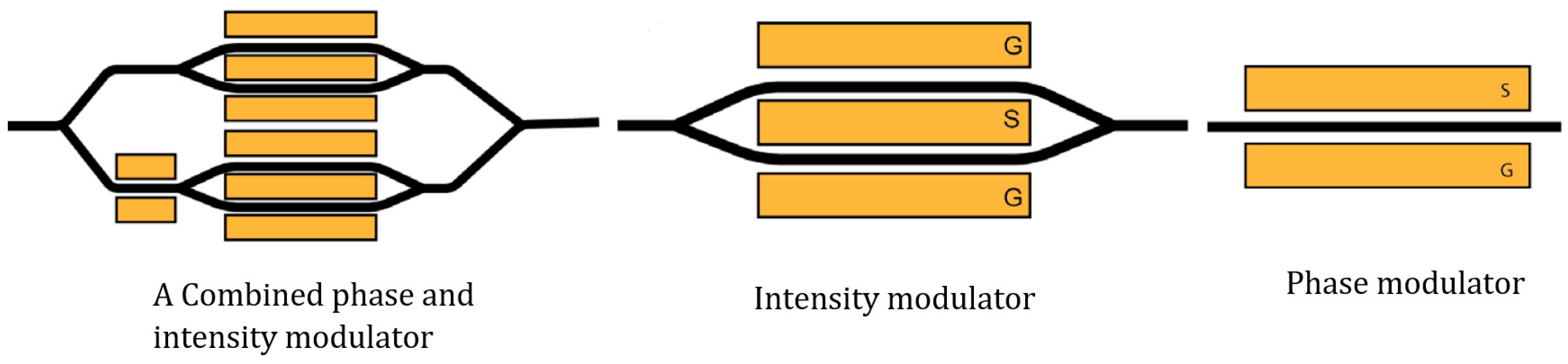
Figure 3 shows the architecture of a light phase modulator, an intensity modulator, and a combined phase and intensity modulator. The intensity modulator is more complicated because it consists of a phase modulator on one arm.

Figure 3.
The architecture of the phase, intensity, and combined phase and intensity modulator.
A CMOS-compatible Mach-Zehnder intensity modulator (MZM) was considered in this design and simulation model. Figure 4 illustrates the configuration of the MZM pursued in this study. Initially, the input optical wave is directed to a directional coupler, where its intensity is evenly split between the two output waveguides. These waveguides constitute the two arms of a Mach-Zehnder interferometer. One of the arms allows for the application of an electric field, enabling the modification of the refractive index in the material and consequently altering the wave’s phase propagating through that specific arm. The two waves are subsequently merged using another 50/50 directional coupler. By adjusting the applied voltage, precise control over the amount of light exiting from the two output waveguides can be achieved.
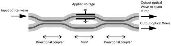
Figure 4.
The structure of the MZM pursued in this study.
As mentioned, six traditional χ(2) materials, including LNB, KNB, LTO, BBO, CdTe, and InP, were considered for this waveguide modulator. In the MZM, a confined mode propagates through one of those six types of EO crystal, and the cladding comprises a doped crystal with a lower index. The optical wavelength (λ) is considered to be 1.55 µm. In order to achieve a state where the field of confined modes exhibits zero magnitude at the exterior boundaries, it is imperative to employ a cladding radius of adequate size. As boundary conditions, it is vital to ensure a rapid decay of the electric field amplitude with respect to the cladding radius coupled with an absolute zero electric field outside the cladding region. These conditions have been implemented to maintain adherence to the prescribed theoretical framework and uphold the integrity of the system under analysis.
In a confined mode, there is no energy flow in the radial direction, making the wave evanescent in the radial direction within the cladding. This condition holds true only if the effective index () is greater than the index of the cladding (). Conversely, the wave cannot be radially evanescent in the core region. Therefore, the effective index must be between the index of the core and that of the cladding (). It is important to note that a higher effective index results in a more confined optical wave, with the fundamental mode having the highest effective index. The effective refractive index of a confined mode is calculated in Equation (1):
where is the vacuum wavenumber, and is the propagation constant. The is a function of the frequency. The normalized frequency of a waveguide or the V-number is calculated in Equation (2):
where a is the radius of the core. The mode analysis is conducted on a cross-sectional plane (xy-plane) of the fiber, specifically examining the behavior of the optical wave in the z-direction. The optical wave can be characterized by the following expression:
Within the provided context, w is defined as 2πν, representing the frequency of the optical wave denoted by ν. In order to determine the eigenvalues for the electric field, the Helmholtz equation (Equation (4)) is solved, yielding the eigenvalues of (−iβ).
In order to model the MZM, the interface for the optical waves’ beam envelopes is formulated by assuming that the electric field can be represented as the product of a slowly varying envelope function and a rapidly varying phase function, as per Equation (5).
In Equation (5), the envelope function, , represents the electric field, where k denotes the wave vector, and r represents the position. When the wave vector k is appropriately chosen for the specific problem, the envelope function, , exhibits spatial variation on a larger length scale compared to the wavelength. In this application, it is reasonable to assume that the wave can be accurately approximated in straight domains by utilizing the wave vector corresponding to the incident mode of β. However, in waveguide bends, assuming α is the bend angle from the x-axis and and are unit vectors in the x and y-directions, the wave vector can be expressed as . Therefore, the wave vector difference in the bent waveguide will be the following:
determines the phase variation for the envelope electric field. The splitting and recombining of light in a guiding mode inside the waveguide is the most complicated task in the model. Steering the incoming photonic intensity toward unusual directions, which is not predicted by Snell’s laws of reflection and refraction in various wavefront engineering applications, can be described with the integral equation formulation presented by Tsitsas and Valagiannopoulos (2020) [14].
The initial step in the model developed in this study is to optimize the waveguide’s bending ratio. This is based on the wavelength, the waveguide’s core, and a width that ensures a 50–50 light split in a guiding mode using a numerical model created in COMSOL multiphysics [15]. This COMSOL model calculates the phase modulation from the optical path difference (OPD) resulting from the change in the index (n) of the EO medium with an appropriate EO coefficient of due to the imposition of an external electric field and the length of propagation (l) through the EO medium under the voltage (V), as per Equation (7) [16].
where D is the distance between the electrodes surrounding the EO medium. The COMSOL model defines the intensity modulation after recombining the two arms if the transmission at the outlet port drops to zero.
The OPD required for modulation in the MZM is expressed as the voltage-length product (Vπ·L) [17]. This value was calculated for each EO material studied based on the assumed geometry. Note that both the choice of EO material and the geometry affect the half-wave voltage (Vπ), causing variations in the voltage-length product for the EO materials examined in this paper.
2.3. Selecting the Type of Electrodes
The lumped or traveling wave (TW) electrodes can be used in the MZM. Lumped MZMs have a smaller length than the wavelength of the modulation field due to the low modulation frequency (f). This results in a longer modulation period (1/f) than the transit time (, which is the duration for the optical wave to propagate through the MZM.
Generally, the 3 dB modulation bandwidth () of an MZM depends on both transit time () and the RC time constant (). Since the RC time is much longer than the transit time in a lumped MZM, the modulation bandwidth is defined by the RC time constant as
For a fixed resistance, the gets longer by increasing the length (l) of the electrodes due to increasing the capacitance by length (). Therefore, . On the other hand, the optical path delay (OPD) increases by length (l) for a given index change, as per Equation (7). Thus, the length of the electrode would be a trade-off between the modulation bandwidth, the required OPD for phase modulation, and the voltage to impose the index change in a lumped MZM; hence, the modulation bandwidth of a lumped MZM cannot be greater than a few gigahertz.
As seen, to achieve higher bandwidth modulation, the lumped modulator’s frequency response is limited by its RC characteristics at high modulation frequencies. In order to overcome this limitation, a traveling wave configuration is used for the MZM. This involves matching the phase velocity of the microwave modulation field or radio frequency (RF) wave with that of the optical wave in the MZM. The MZM with traveling wave-type electrodes is called TW-MZM [18]. This type of electrode was selected for the MZM in this study.
In order to enable effective interaction between the microwave field and optical wave in a TW-MZM, the high-frequency modulation signal is injected and propagates in the same direction as the optical wave, terminating at the end of the electrode transmission line [19].
The modulation bandwidth of a TW-MZM depends on the mismatch between the phase-velocity of the optical wave propagating in the waveguide and the RF wave propagating in the transmission line, as well as the loss of RF signal along the transmission line depending on the frequency of the RF wave. The velocity mismatch and the RF attenuation also depend on the materials and geometry of the waveguide and the transmission line [4]. Considering Z as the impedance of the transmission line (, L as inductance, C as capacitance per unit of length of transmission line, as the index for the RF wave, and as the effective index of the optical wave, the phase velocity of the RF () and the optical wave in the guided mode () can be calculated as
Considering the frequency-dependent absorption coefficient of α for the RF wave in the transmission line, the voltage attenuation coefficient will be 0.5 α, and therefore, the traveling voltage throughout the electrode as a function of time and space will be
where is the peak of the modulation voltage, and is the angular modulation frequency. That variation in voltage in time and space will impose a variable change in the propagation in time, space, and also frequency due to the dependence of the phase velocity of RF on frequency (). The would impose the maximum electric field to the EO medium and achieve the maximum index change () and, therefore, the maximum change in the propagation constant ().
The max change in the propagation constant results in the max phase shift ():
The optical wave entering the entrance port at the time of t will get to the point of z at , where the voltage at that point is Therefore, the change in the propagation constant will be
Therefore, the phase modulation will be
In order to estimate the maximum modulation bandwidth of TW-MZM, two limitation cases can be considered: having a velocity mismatch between the RF and optical waves () but a very low loss transmission line (α ≈ 0), as in Case 1, and having minimum velocity mismatch () but a lossy transmission line (), as in Case 2.
- i.
- Case 1: The phase modulation in this case is
After conducting a lengthy analytical calculation, one can demonstrate that the modulation bandwidth of the TW-MZM, in this case, is calculated as follows:
The equation above shows that achieving velocity matching between RF and optical waves in a TW-MZM using a low-loss transmission line can significantly increase modulation bandwidth. Employing low-loss RF transmission methods, such as radio-over-fiber (RoF) [20] techniques, in such systems further enhances this effect, leading to exceptionally high modulation bandwidth.
- ii.
- Case 2: The phase modulation in this case is
Therefore, in this case, the modulation bandwidth of the TW-MZM will be inversely proportional to the square of the length.
Therefore, if the phase velocity of the RF and optical waves in a TW-MZM are matched, the modulation bandwidth will be limited solely by the square of the length of the transmission line.
However, the transmission line cannot be too short due to the necessary OPD for phase modulation. In order to meet the OPD requirements while reducing the transmission line length, exhibiting a medium with a higher index change will be advantageous.
2.4. Velocity Matching between the RF and Optical Wave
As mentioned, the optical wave’s group velocity and the microwave’s phase velocity must be matched to increase the modulation bandwidth. The maximum bandwidth of the TW-MZM will be the frequency of the RF wave, which has a phase velocity matched to the group velocity of the optical wave [7].
The velocity of the optical wave is defined by the optical wave’s effective index in the waveguide, which is defined by wavelength(s), the propagation mode, the core size, and the refractive index of the core and cladding, which can be calculated independently of RF propagation. On the other hand, the RF phase velocity is a function of substrate thickness and the type and size of the electrodes, cladding sizes, and refractive indices, which can be modeled after calculating the optical wave propagation. Therefore, the materials and the thickness of the SiO2 can be controlled to get the velocity of the RF and optical waves matched together, as schematically shown in Figure 5.
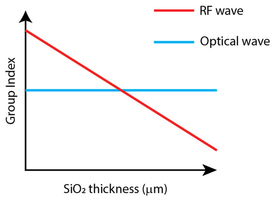
Figure 5.
Adjusting the SiO2 layer thickness enables velocity matching between the RF and optical waves.
The thickness of the SiO2 layer in a TW-MZM, as depicted in Figure 1a, does not impact the optical wave’s propagation constant. However, it does affect the phase velocity of the RF wave. Adjusting the SiO2 layer’s thickness makes it possible to achieve velocity matching between the optical and RF waves to optimize the modulation bandwidth.
As shown in Figure 1a, it is essential to note that the SiO2 layer in the TW-MZM considered in this study is not positioned on top of the nonlinear layer, unlike conventional MZMs. Therefore, altering the SiO2 thickness does not affect the propagation constant of the optical wave; instead, it solely controls the propagation constant of the RF wave (Figure 5).
Wang et al. (2018) and Pascher et al. (2003) [7,13] conducted similar studies, where they optimized the SiO2 layer thickness in a thin-film TW-MZM to attain velocity matching between the RF and optical waves to maximize the modulation bandwidth. Wang et al. (2018) [13] focused on a TW-MZM with an assumed geometry and LNB as the EO medium, while Pascher et al. (2003) [7] explored a different geometry using InP as the EO medium.
2.5. The Loss Estimation Method for the RF and Optical Waves in the TW-MZM
In the TW-MZM depicted in Figure 4, the input optical wave, characterized by a known intensity, is introduced through one of the inlet ports. The COMSOL model can compute the intensity of the outgoing light from both outlet ports. Consequently, the optical loss can be determined as the disparity between the input and output intensities. This variation can be visually presented by plotting the optical loss along the length of the directional coupler waveguide.
Although the calculation of optical loss, as described earlier, appears straightforward, determining the loss of the radio frequency (RF) wave is more complex and requires evaluating the RF propagation constant following velocity matching. Assuming the complex RF propagation constant is , the RF field will be
As the intensity of the radio frequency (RF) wave is directly proportional to the square of the field, the RF intensity follows an exponential decay as per the Beer–Lambert law.
Therefore, the RF absorption coefficient will be and is reported in terms of dB/mm.
In this model developed in COMSOL multiphysics, the loss associated with the RF wave is computed as described above for the six EO crystals under investigation. The calculations involve optimizing the shape and adjusting the thickness of the silicon dioxide layer (or the silicon layer in the case of CdTe) to achieve a velocity matching between the RF and optical waves, and the results will be compared.
2.6. Modeling in COMSOL Multiphysics
The model developed in COMSOL multiphysics [15] defines the fundamental mode of the optical wave propagating through the TW-MZM based on the geometry, structure, and EO medium used in the waveguide. Then, the cross-section of that TW-MZM with a variable SiO2 thickness is used to adjust the propagation constant and the phase velocity of the RF wave to match the optical wave group velocity. Since the propagation constant of the RF depends on its frequency and the size and structure of the TW-MZM designed in the previous section, only the SiO2 thickness, which does not affect the propagation constant of the optical wave, is optimized for each RF frequency in order to match the velocity of the RF and optical waves. The model can find an RF frequency with the same phase velocity as the optical wave to define the maximum bandwidth of modulation associated with the EO medium selected.
2.6.1. The Inputs of the Model
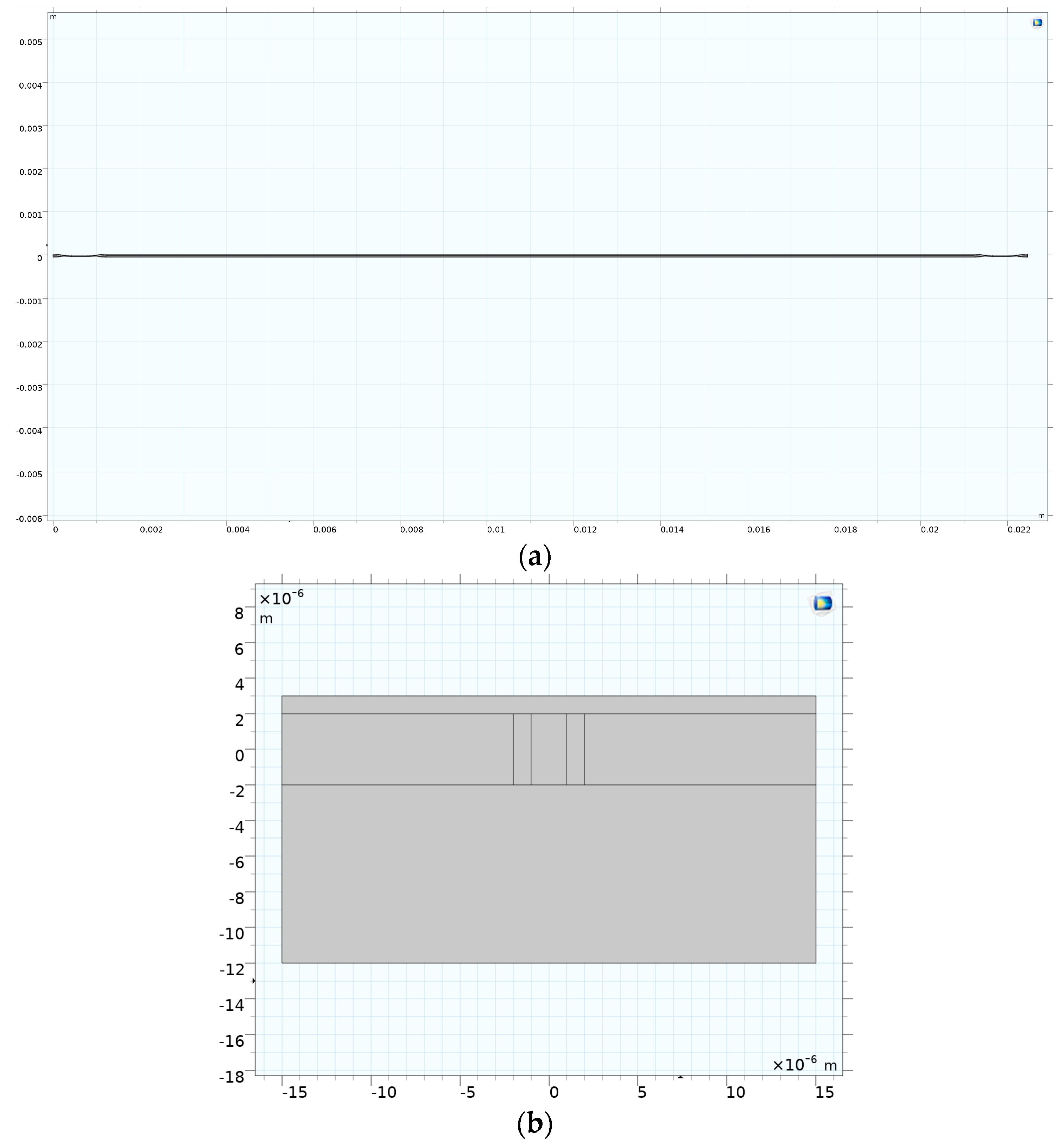
As mentioned, a TW-MZM with a specific geometry is considered in this model. Figure 6 shows the top view and the section view of the TW-MZM.
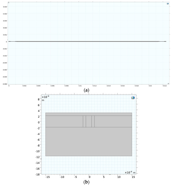
Figure 6.
The top view (a) and the section view (b) of the TW-MZM considered in this model.
As seen in the top view of the TW-MZM (Figure 6a), this TW-MZM has four ports. One port on the right side is the input, and the other is a dummy port for ease of modeling. On the left side, one port is the output, and the other is connected to a beam dump. As seen, the light enters the device from one port on the right side and is split into two arms while one arm is under an external electric field, and the medium is electro-optically activated for phase modulation. Then, the two arms get recombined. The intensity of the light in the output part is modulated by changing the voltage applied to the electrodes. Changing the applied voltage will alter the external electric field and the refractive index of the EO material on one arm, leading to a phase delay on one arm. Recombining the phased modulated light in one arm with the light propagating in the other will cause destructive or constructive interference between the lights, resulting in intensity modulation at the output port.
The light is propagated inside the core, and an evanescent field exists in the cladding. The RF wave, on the other hand, propagates beyond the core; therefore, the other layers and electrodes become essential to calculate the propagation constant of the RF wave. Figure 6b shows the cross-section of the TW-MZM modulating arm, which is used to calculate the propagation constant of the RF wave.
The top layer in Figure 6b is made of air; the electrodes are made of gold, and the substrate is SiO2 for the EO crystals investigated in this study, except CdTe. The core is made of an EO material, and the cladding has a slightly lower index.
The list of the inputs of the model is given in Table 2. The input data in Table 2 uses LNB as the EO medium, just as an example.
Table 2.
The list of inputs for the TW-MZM simulation and design model.
2.6.2. The Two Steps of the Model
The design and simulation of a TW-MZM are conducted in this model via the two following steps:
- i.
- Step 1–The optical wave side: In this step, the top view of the modulator is considered (Figure 6a), and the geometry is constructed according to the inputs (Table 2). The parameters calculated in this step are as follows:
- The propagation constant of the fundamental mode for the optical wave;
- The effective index of the fundamental mode for the optical wave;
- The voltage length product for each EO material based on the assumed geometry;
- The transmission, reflectance, and loss in all ports at the given range for the applied voltage;
- The optical guided field at all ports under different applied voltages.
Having the effective index or group velocity of the optical wave makes it possible to optimize the SiO2 layer (or Si layer in the case of CdTe) thickness of the TW-MZM to get the phase velocity of the RF wave equal to the group velocity of the optical wave. These calculations are performed in the second step as follows:
- ii.
- Step 2–The RF wave side: In this step, the section view of the modulator (Figure 6b) is considered, and the geometry is constructed according to the inputs. Then, the thickness of the SiO2 layer (or Si layer in the case of CdTe) is optimized for every single RF frequency in the given range to minimize the difference between the effective indices of the fundamental mode of the RF and optical waves propagating through the TW-MZM. The parameters calculated in this step are as follows:
- By optimizing the SiO2 layer (or the Si layer in the case of CdTe) thickness for every RF frequency, the propagation constant, the effective index, and the phase velocity of the RF wave at that frequency are calculated;
- The RF field at every frequency is evaluated by optimizing the SiO2 layer (or Si layer in the case of CdTe) thickness for every RF frequency;
- The effective index of the fundamental mode of the RF wave after optimizing the thickness of the SiO2 is plotted versus the frequency of the RF wave;
- The maximum bandwidth of the modulation, as the frequency of the RF wave with the fundamental mode effective index matching to the optical wave’s fundamental mode effective index, is estimated;
- The RF loss coefficient is calculated using the imaginary part of the RF propagation constant resulting from the velocity matching.
The performance of the TW-MZM and the maximum bandwidth both depend on the type of EO material used for modulation and the modulator’s geometry and structure. This model was run using six different EO materials, and the performance results, including the loss and maximum bandwidth of modulation associated with each EO material after optimization of the selected geometry for velocity matching, were evaluated.
3. Results and Discussions
3.1. The Results of the Model When Using Lithium Niobate (LNB) as the EO Medium
Lithium Niobate (LNB), a ferroelectric crystal with uniaxial birefringence, is commonly utilized for waveguide fabrication. The waveguide structures can be created through two methods: the indiffusion of titanium (Ti) into the core regions or annealed proton exchange. In the indiffusion process, titanium is diffused into specific areas of the crystal’s core. On the other hand, annealed proton exchange involves exchanging lithium ions with protons from an acid bath. Both approaches enable the formation of waveguides in lithium niobate.
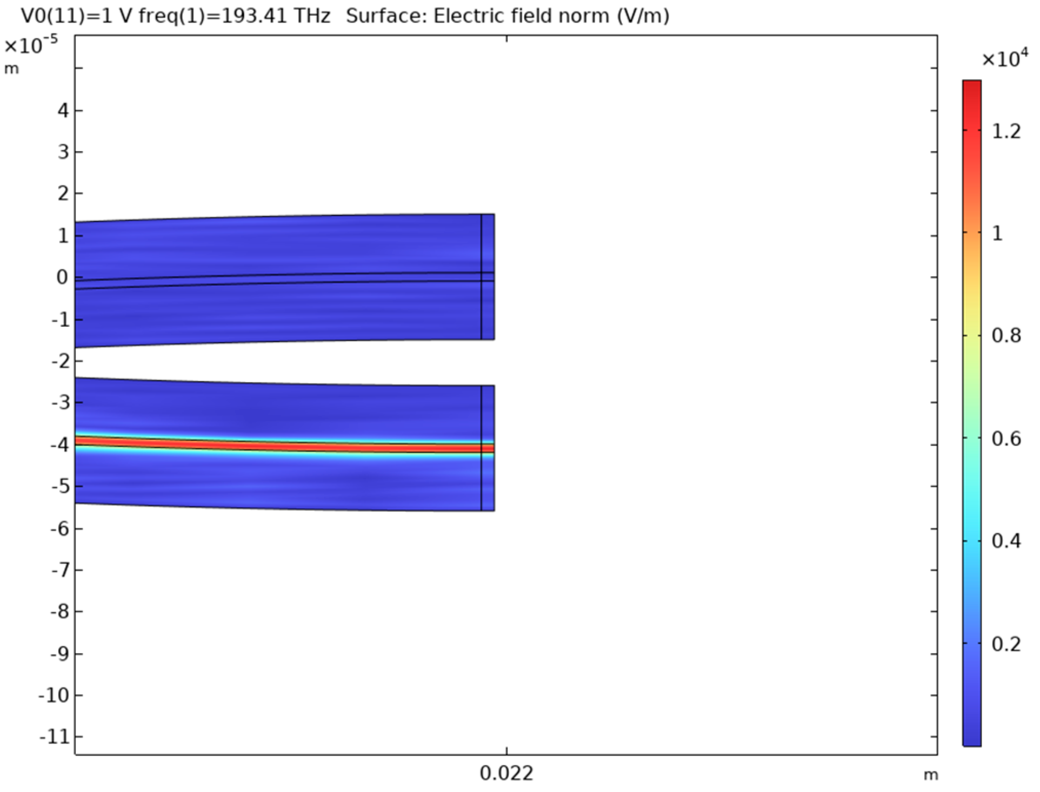
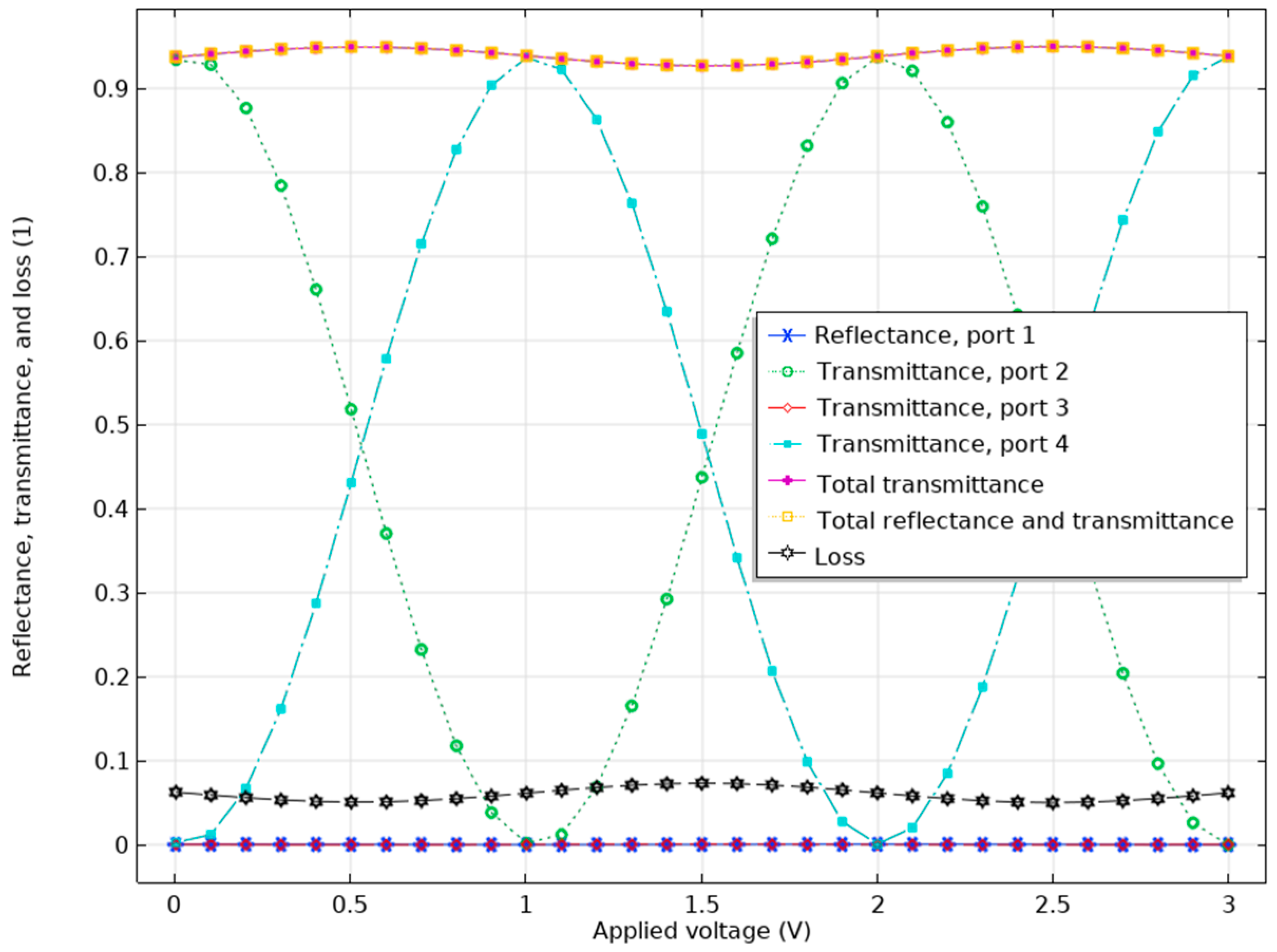
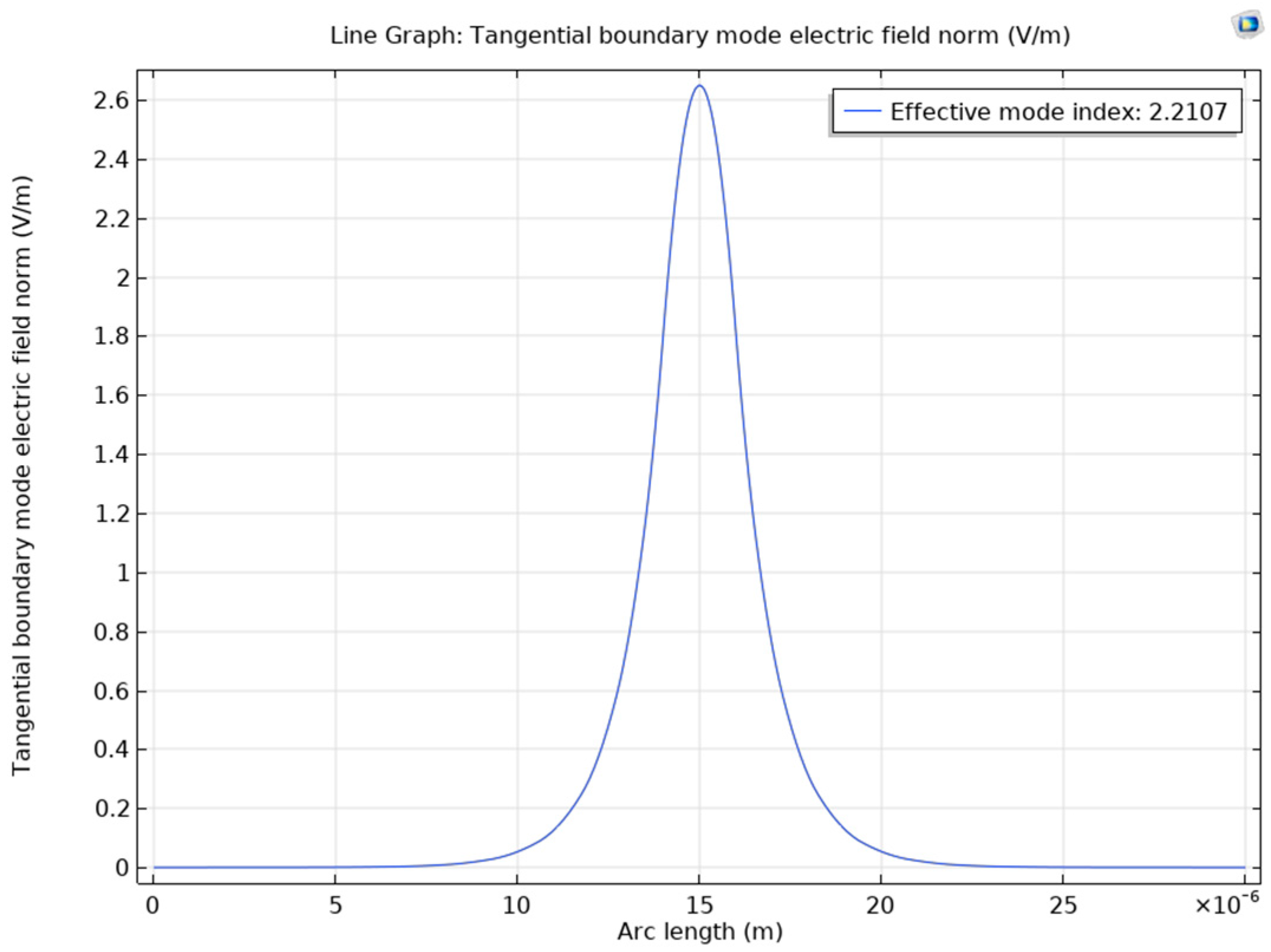
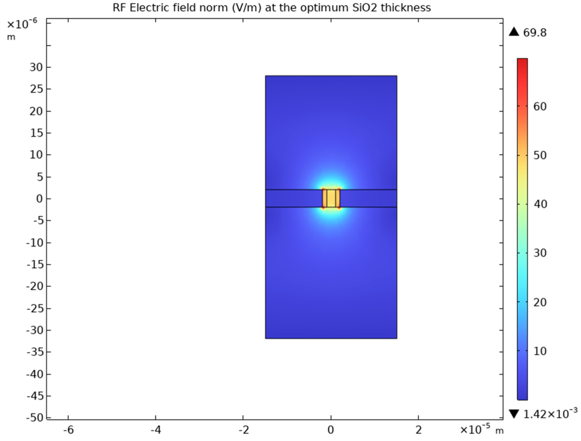
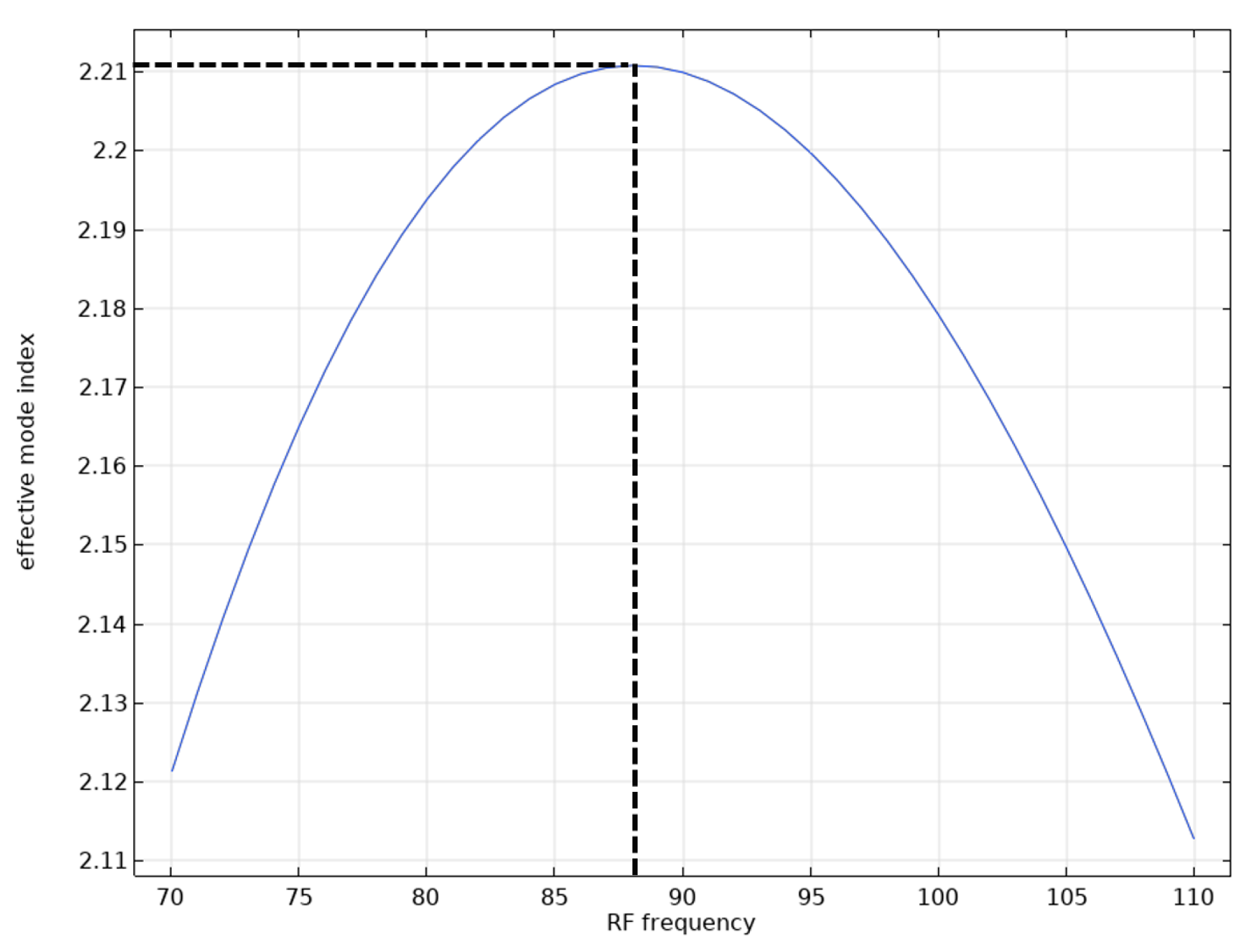
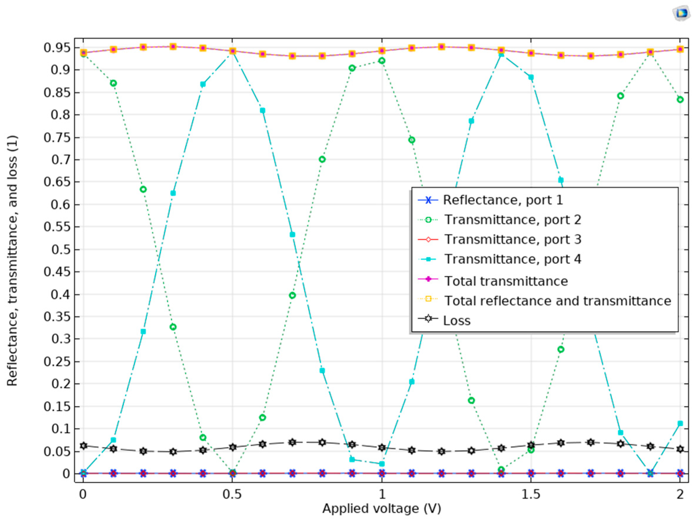
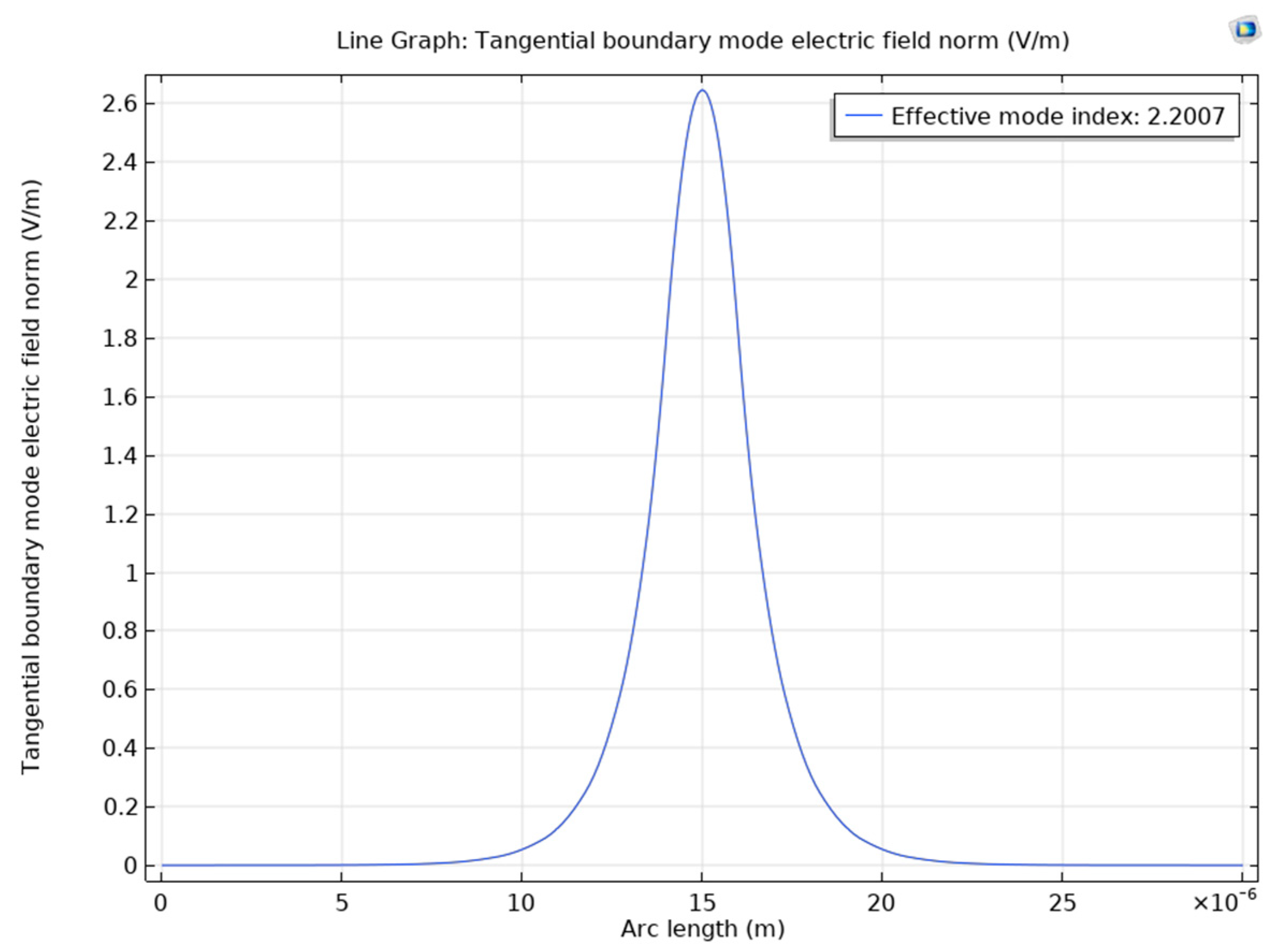
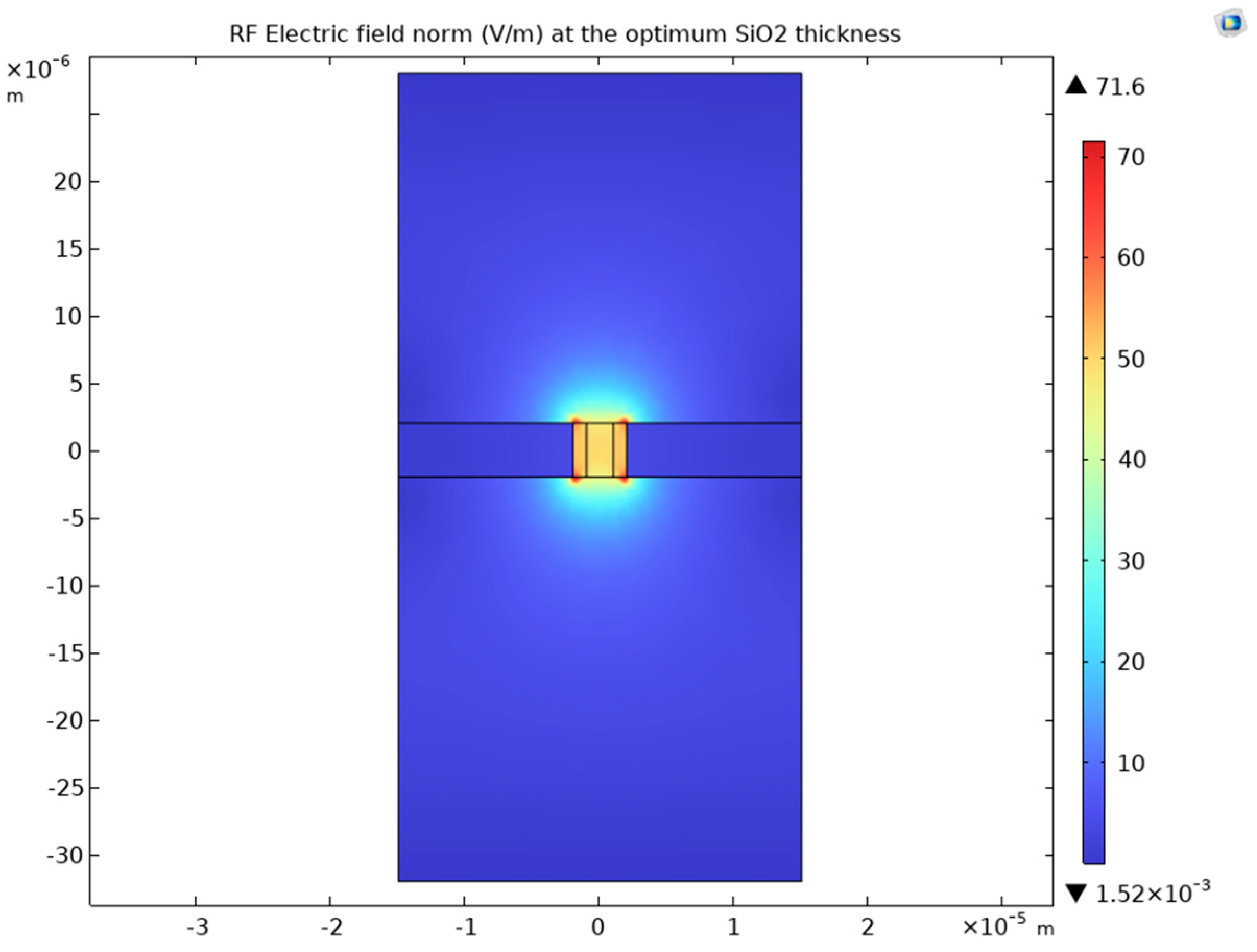
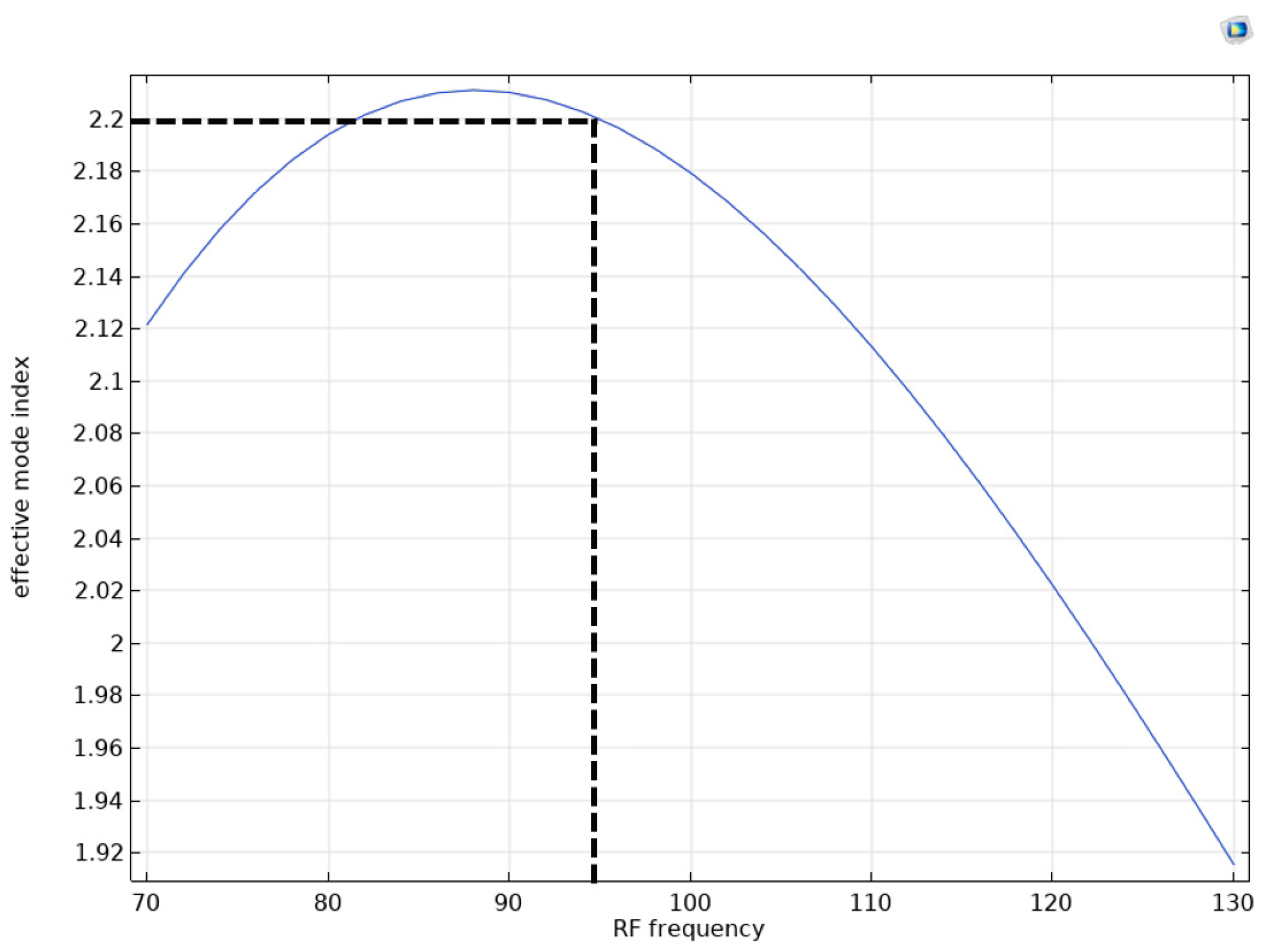
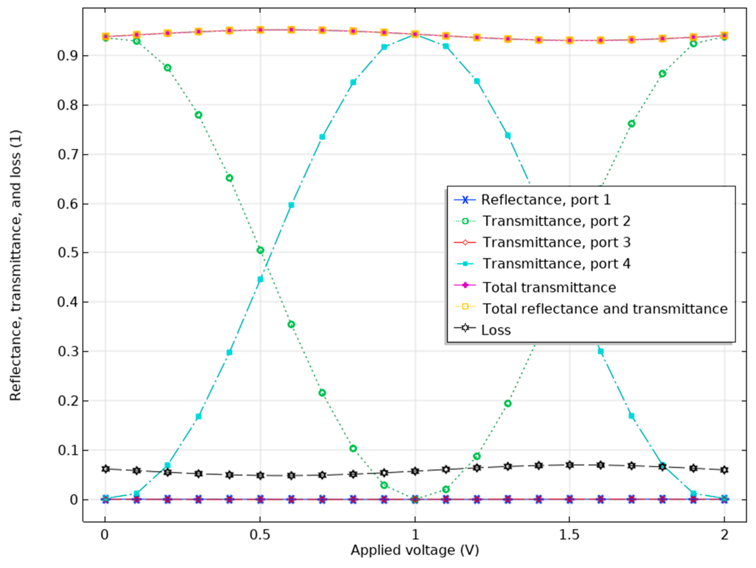
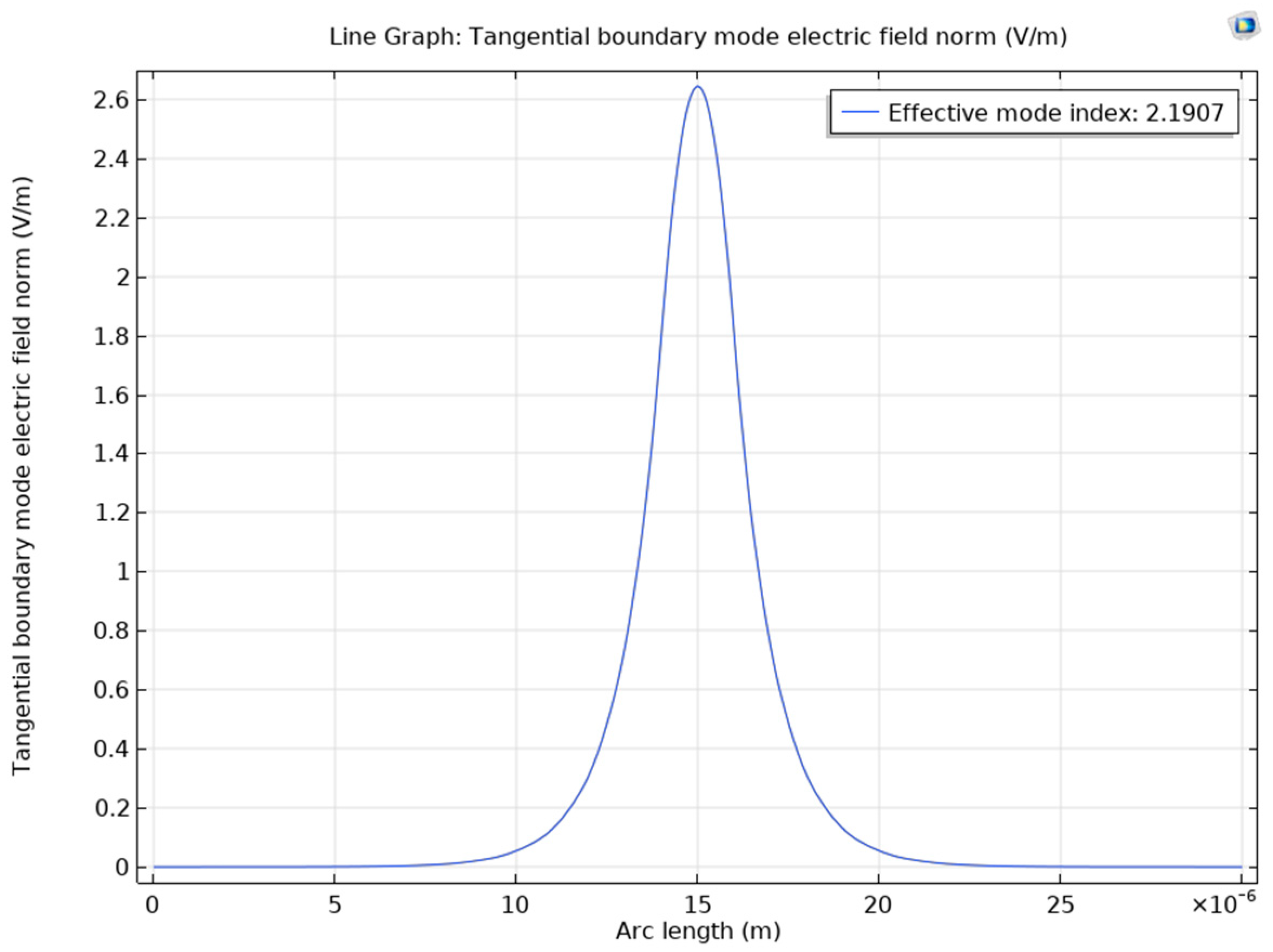
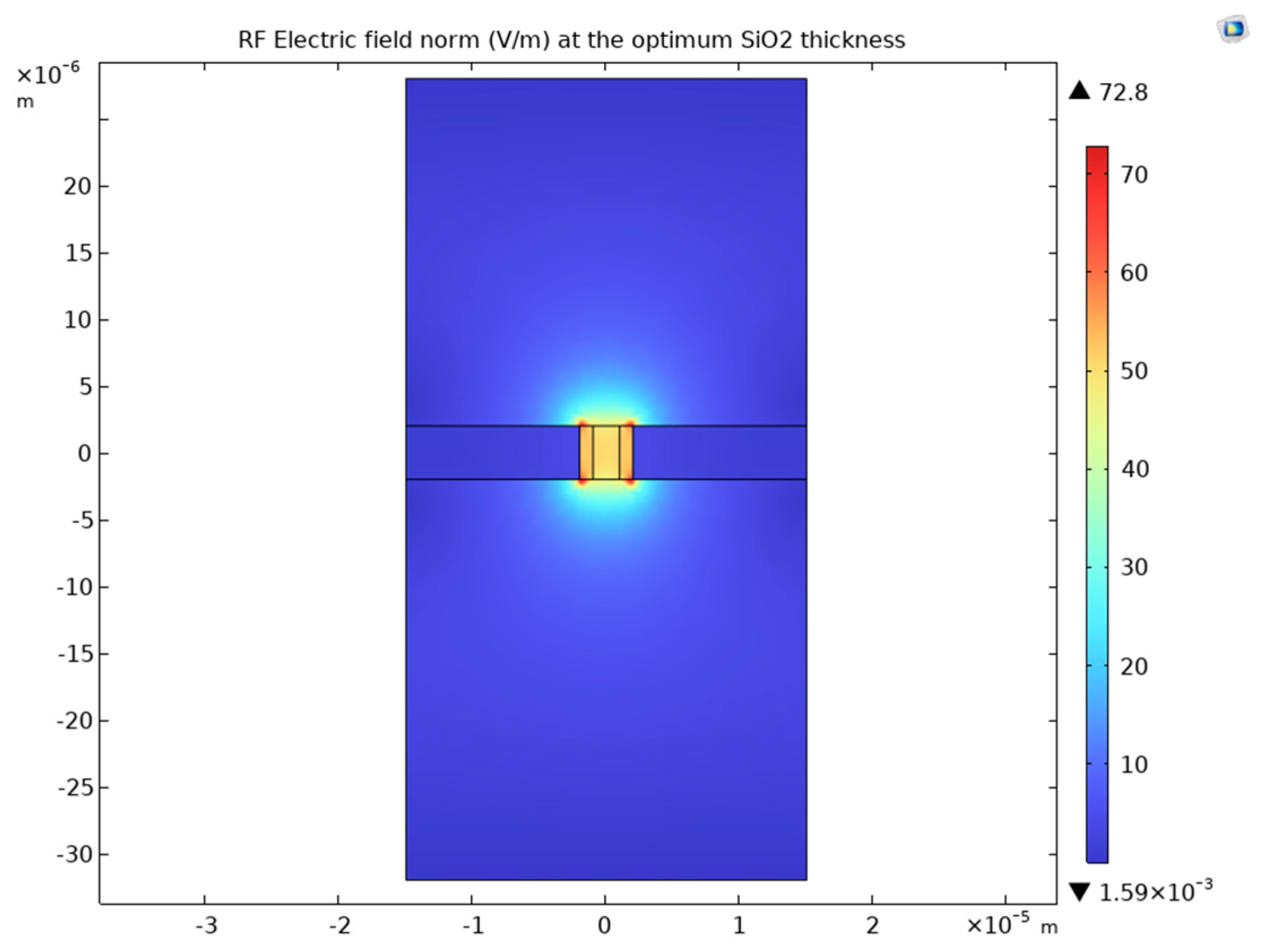
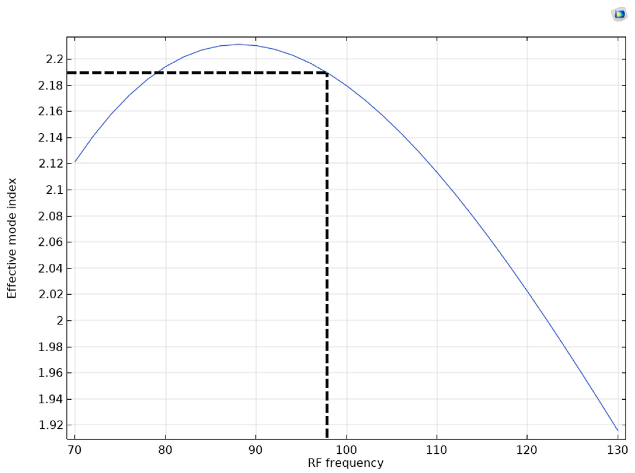
Table 3 shows the model output for using LNB as the EO material in the TW-MZM. The optical field at the output port under the voltage of 1 V is given in Figure 7. The transmission, reflection, and loss in all ports for all applied voltages within the voltage range are given in Figure 8. The fundamental mode of the optical wave and its effective index are shown in Figure 9. The RF field at the optimum frequency is given in Figure 10. The effective index of the fundamental mode of the RF wave versus the RF frequency is given in Figure 11.
Table 3.
The output of the model for LNB as the EO material in this TW-MZM.
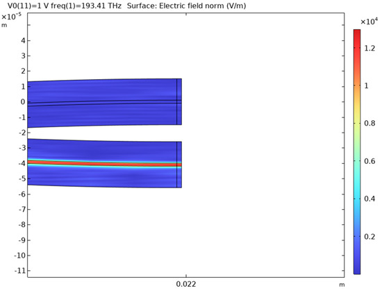
Figure 7.
The optical field at the output port under a voltage of 1 V for LNB.
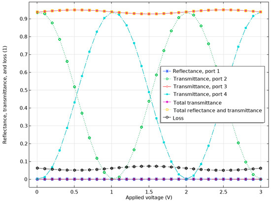
Figure 8.
The transmission, reflection, and loss in all ports for all applied voltages within the voltage range for LNB.
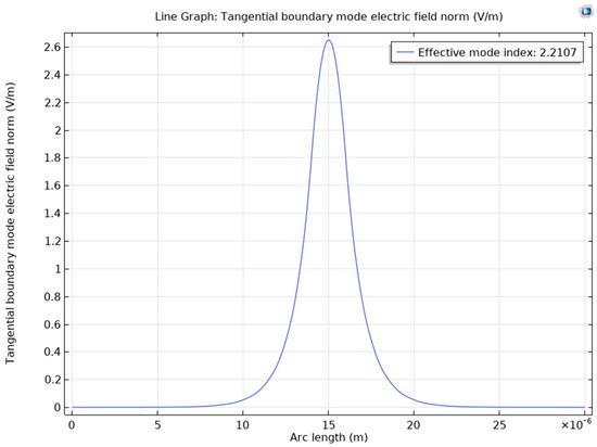
Figure 9.
The fundamental mode of the optical wave and its effective index for LNB.

Figure 10.
The RF field at the optimum frequency for LNB.
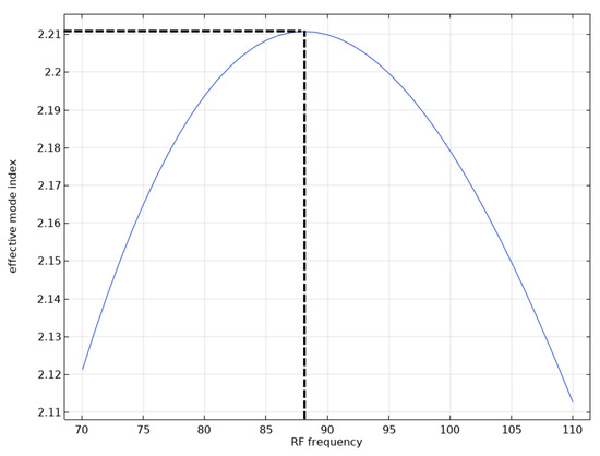
Figure 11.
The effective index of the fundamental mode of the RF wave versus the RF frequency for LNB.
As shown in Figure 11, the effective index of the RF wave with an 88GHz frequency is matched to the effective index of the optical wave. Therefore, the maximum modulation bandwidth for using LNB as the EO medium in this specific geometry after the optimization for velocity matching would be 88GHz.
3.2. The Results of the Model When Using BBO as the EO Medium
Table 4 shows the model output for using BBO as the EO material in the TW-MZM. The fundamental mode of the optical wave and its effective index are shown in Figure 12. The RF field at the optimum frequency is given in Figure 13. The effective index of the fundamental mode of the RF wave versus the RF frequency is given in Figure 14.
Table 4.
The output of the model for BBO as the EO material in this TW-MZM.
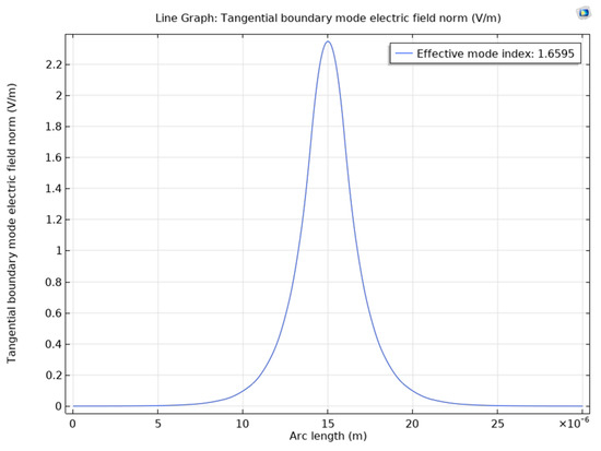
Figure 12.
The fundamental mode of the optical wave and its effective index for BBO.

Figure 13.
The RF field at the optimum frequency for BBO.
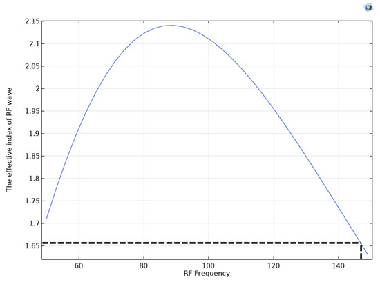
Figure 14.
The effective index of the fundamental mode of the RF wave versus the RF frequency for BBO.
As shown in Figure 14, the effective index of the RF wave with a 148 GHz frequency is matched to the effective index of the optical wave. Therefore, the maximum modulation bandwidth for using BBO as the EO medium in this geometry would be 148 GHz.
3.3. The Results of the Model When Using Potassium Niobate (KNB) as the EO Medium
Table 5 shows the model output when using KNB as the EO material in the TW-MZM. The transmission, reflection, and loss in all ports for all applied voltages within the voltage range are given in Figure 15. The fundamental mode of the optical wave and its effective index are shown in Figure 16. The RF field at the optimum frequency is given in Figure 17. The effective index of the fundamental mode of the RF wave versus the RF frequency is given in Figure 18.
Table 5.
The output of the model for KNB as the EO material in this TW-MZM.
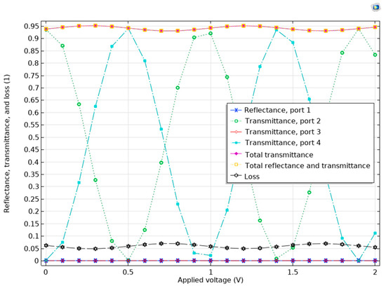
Figure 15.
The transmission, reflection, and loss in all ports for all applied voltages within the voltage range for KNB.
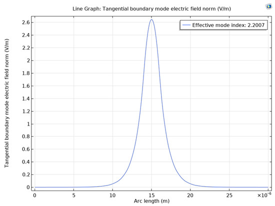
Figure 16.
The fundamental mode of the optical wave and its effective index for KNB.
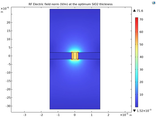
Figure 17.
The RF field at the optimum frequency for KNB.
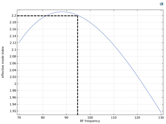
Figure 18.
The effective index of the fundamental mode of the RF wave versus the RF frequency for KNB.
As shown in Figure 18, the effective index of the RF wave with a 94 GHz frequency is matched to the effective index of the optical wave. Therefore, the maximum modulation bandwidth for using KNB as the EO medium in this geometry would be 94 GHz.
3.4. The Results of the Model When Using LiTiO3 as the EO Medium
Table 6 shows the model output for using LTO as the EO material in the TW-MZM. The transmission, reflection, and loss in all ports for all applied voltages within the voltage range are given in Figure 19. The fundamental mode of the optical wave and its effective index are shown in Figure 20. The RF field at the optimum frequency is given in Figure 21. The effective index of the fundamental mode of the RF wave versus the RF frequency is given in Figure 22.
Table 6.
The output of the model for LTO as the EO material in this TW-MZM.
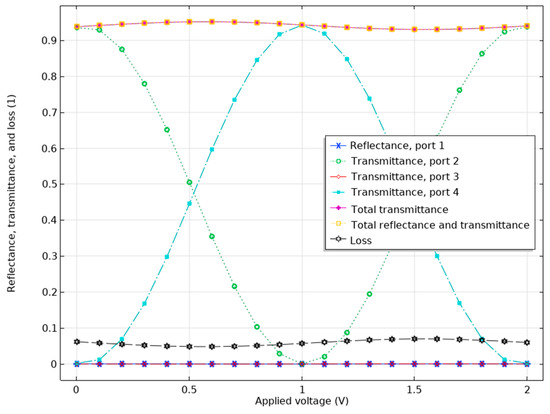
Figure 19.
The transmission, reflection, and loss in all ports for all applied voltages within the voltage range for LTO.

Figure 20.
The fundamental mode of the optical wave and its effective index for LTO.
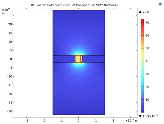
Figure 21.
The RF field at the optimum frequency for LTO.
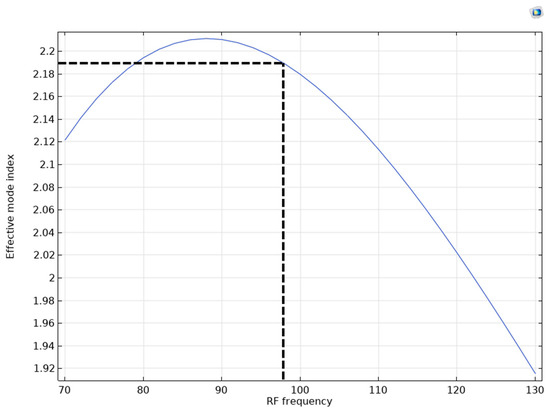
Figure 22.
The effective index of the fundamental mode of the RF wave versus the RF frequency for LTO.
As shown in Figure 22, the effective index of the RF wave with a 97 GHz frequency is matched to the effective index of the optical wave. Therefore, the maximum modulation bandwidth for using LTO as the EO medium in this geometry would be 97 GHz.
3.5. The Results of the Model When Using CdTe as the EO Medium
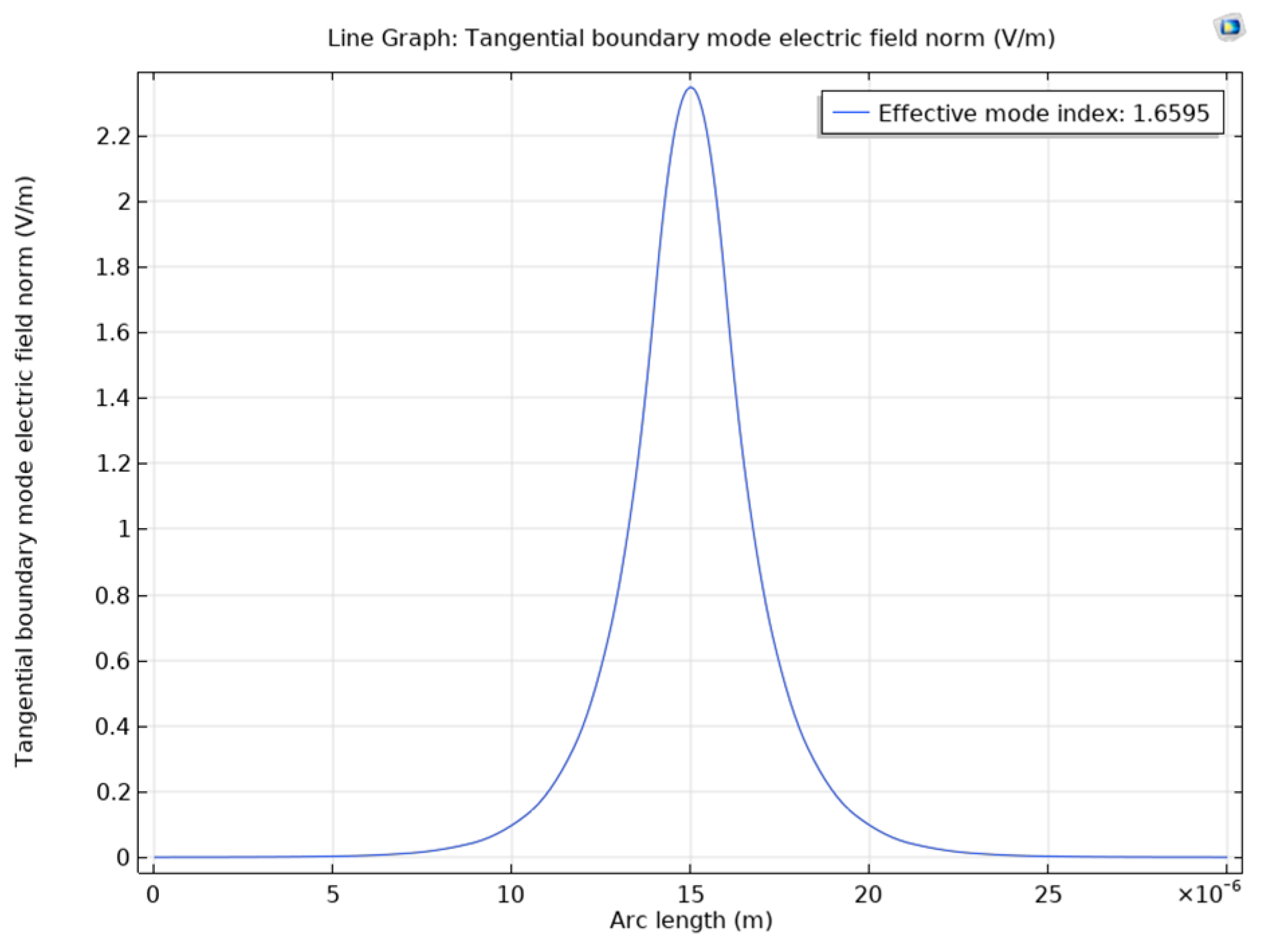
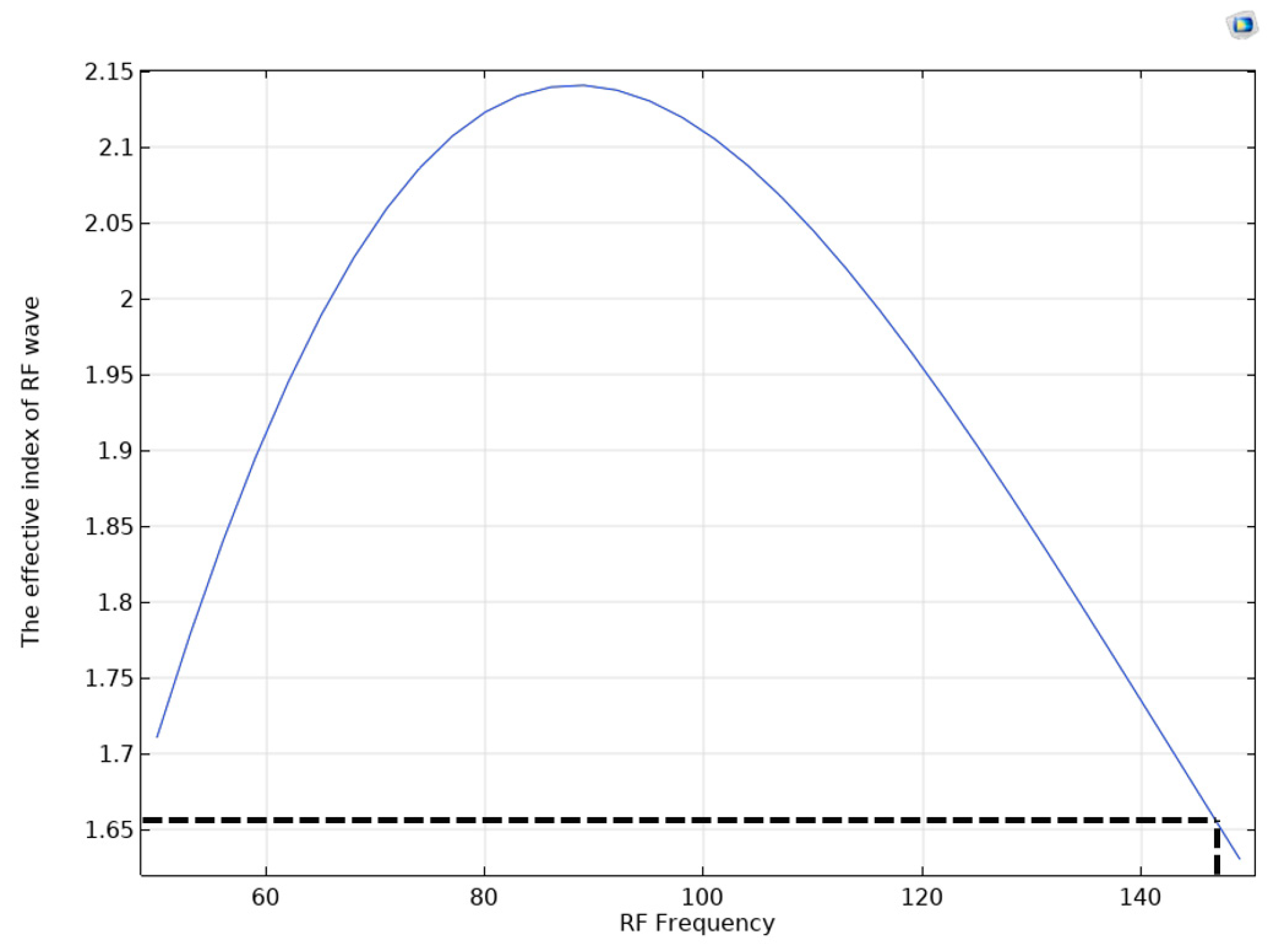
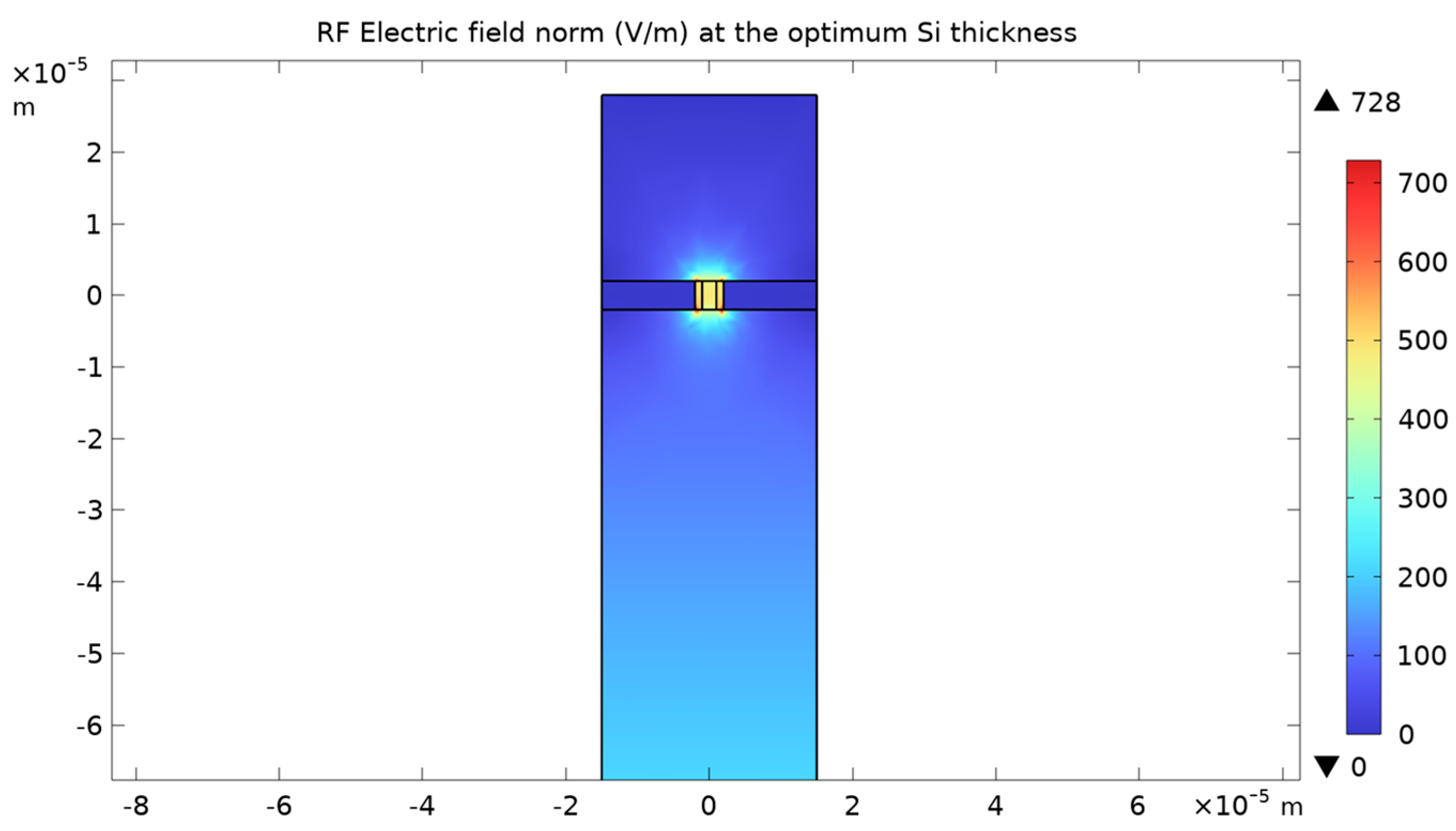
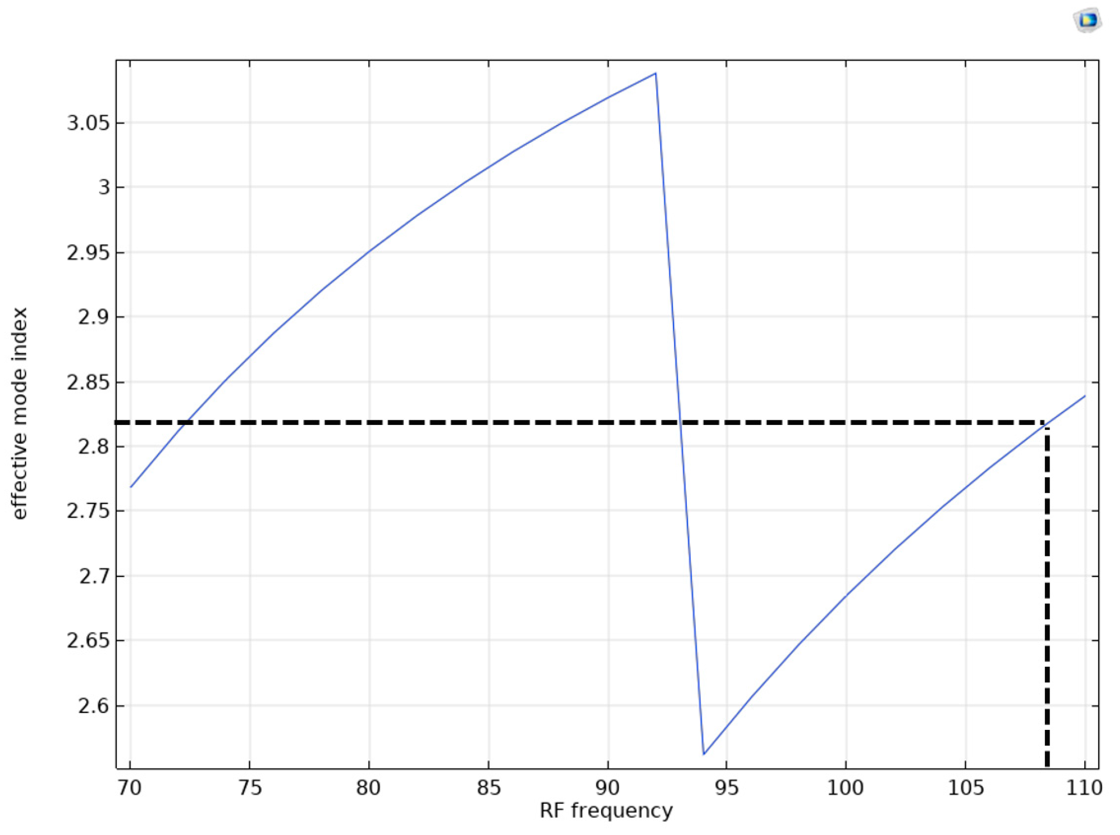
The assumed geometry in this model does not converge when employing CdTe as the EO medium. The reason for that is the CdTe is a high index semiconductor, and adjusting the thickness of the SiO2 layer will not make the phase velocity of the RF wave low enough to match the group velocity of the optical wave. Therefore, to examine the performance of CdTe as the EO material in this TW-MZM, we needed to replace the SiO2 layer with a Si layer and try to optimize the thickness of the Si layer to get a velocity match between the RF and optical wave to estimate the maximum modulation bandwidth of the TW-MZM in the case of using CdTe as the EO medium and Si as the substrate. The fundamental mode of the optical wave and its effective index are shown in Figure 23. The RF field at the optimum frequency after the optimization of the thickness of the Si layer is given in Figure 24. The effective index of the fundamental mode of the RF wave versus the RF frequency is given in Figure 25.
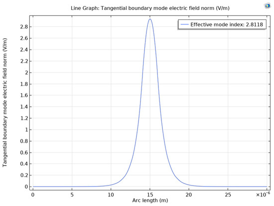
Figure 23.
The fundamental mode of the optical wave and its effective index for CdTe.
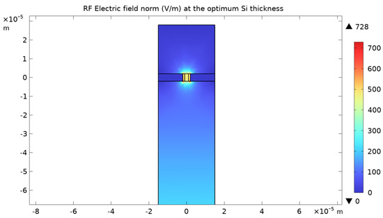
Figure 24.
The RF field at the optimum frequency after the optimization of the thickness of the Si layer for CdTe.

Figure 25.
The effective index of the fundamental mode of the RF wave after the optimization of the thickness of the Si layer for each frequency versus the RF frequency for CdTe.
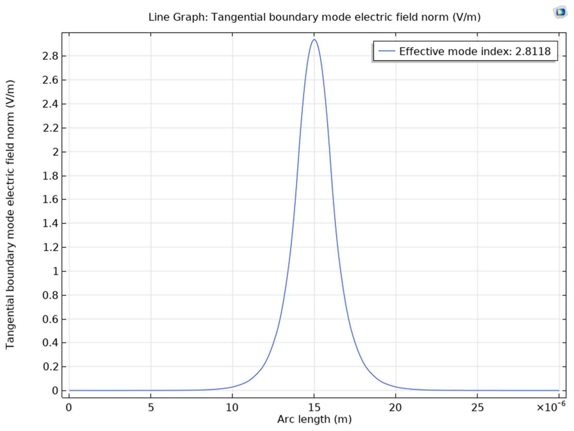
As mentioned, using CdTe as the EO material in the geometry assumed for the TW-MZM presented challenges, and the optimization model failed to converge. That is because adjusting the SiO2 layer thickness did not sufficiently lower the RF wave’s phase velocity to match the optical wave’s group velocity. Consequently, we replaced the SiO2 layer with a Si layer and adjusted its thickness accordingly. Figure 25 illustrates the matching of the effective index of the RF wave at a frequency of 108 GHz with that of the optical wave. Hence, the maximum modulation bandwidth achievable using CdTe as the EO medium in this setup is 108 GHz.
3.6. The Results for Using InP as the EO Medium Calculated by Pascher et al. [7]
The assumed geometry in this model (Figure 6) did not converge when utilizing indium phosphide (InP) as the EO medium. Consequently, to investigate the possibility of employing InP as the EO material in a TW-MZM and evaluate its performance, the results published by Pascher et al. (2003) [7] were referred to in this study.
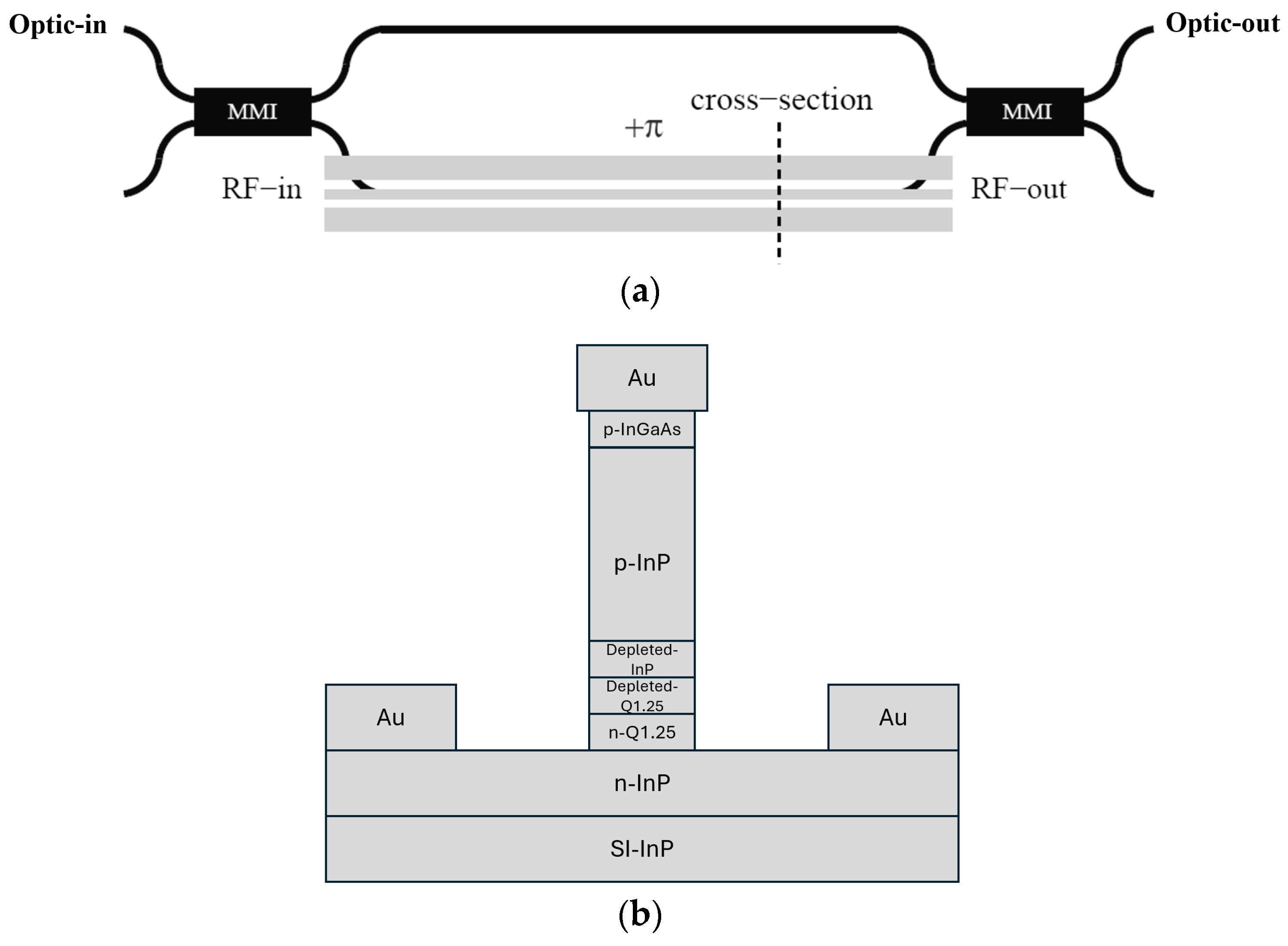
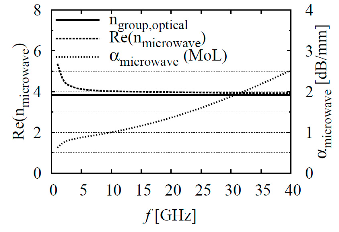
Figure 26 presents the top and sectional views of the TW-MZM, as examined in the study conducted by Pascher et al. (2003) [7]. Figure 27 shows the RF attenuation (α) and the real part of the RF index for the TW-MZM optimized for InP by Pascher et al. (2003) [7].
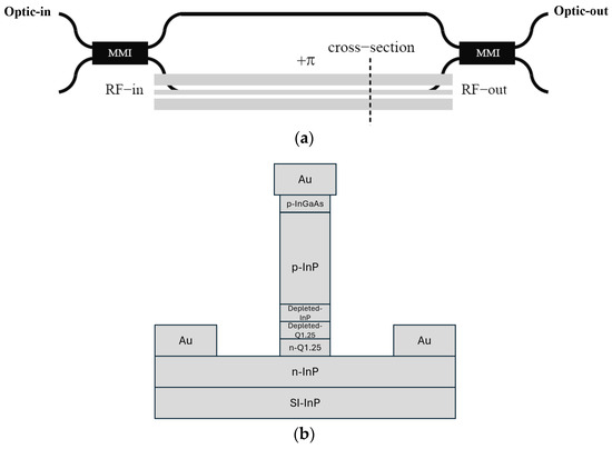
Figure 26.
The top view (a) and the section view (b) of the TW-MZM that was considered by Pascher et al. (2003) [7].
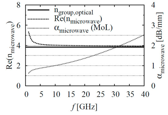
Figure 27.
The RF attenuation (α) and the real part of the RF index for the TW-MZM optimized for InP by Pascher et al. (2003) [7].
As seen in Figure 27, which was presented by Pascher et al. (2003) [7], the real part of the effective index of the RF wave, at an approximate frequency of 40 GHz, aligns with the effective index of the fundamental mode of the optical wave. Accordingly, within the optimized geometry proposed by Pascher et al. (2003), the potential maximum modulation bandwidth achievable when employing InP as the EO medium would be 40 GHz [7].
3.7. Comparing the Bandwidth, Optical Loss, and RF Loss of the TW-MZM Optimized for Each of the Six EO Crystals
This study investigated the suitability of six different EO materials, including LNB, BBO, KNB, LTO, CdTe, and InP, to be used as an EO medium in a traveling wave Mach-Zehnder intensity modulator. Considering an optical wavelength of 1.55 μm and utilizing the specific structure described in this report after optimization for velocity matching, we present the key performance results for each of the six EO materials in Table 7.
Table 7.
Performance comparison of six EO materials in the TW-MZM after optimization for velocity matching.
4. Conclusions
In addition to the type of electro-optical (EO) crystal, the performance of a traveling wave Mach-Zehnder intensity modulator (TW-MZM) is also greatly influenced by the selected geometry and materials employed in other layers. This study aimed to evaluate the effects of different EO materials on the performance of the TW-MZM, with specific optimizations carried out for each of the six EO materials. In the case of CdTe utilization, the SiO2 layer was substituted with a Si layer, and the thickness of the Si layer was optimized instead of the SiO2 layer thickness. The assumed geometry in this model did not converge for InP; therefore, the results calculated by Pascher et al. (2003) [7] were presented and compared to the other five EO materials.
The results indicated that KNB, LTO, BBO, and CdTe have the potential to surpass LNB in terms of a higher modulation bandwidth. However, it should be noted that KNB and LTO demonstrate a comparable level of loss compared to LNB. The findings demonstrate that BBO and, specifically, CdTe exhibit modulation bandwidths exceeding 100 GHz while exhibiting the lowest loss among the considered crystals based on the adopted geometry. The results of Pascher et al. showed that although InP exhibits the lowest RF loss, the associated modulation bandwidth is much lower than what can be achieved with the other five crystals.
Future studies will explore alternative geometries and different materials for other layers, aiming to define an optimal configuration that maximizes modulation bandwidth and minimizes optical and RF loss.
Author Contributions
Conceptualization, A.A. and P.M.; methodology, A.A. and P.M.; software, A.A. and A.S.; validation, A.A., P.M. and A.S.; formal analysis, A.A.; investigation, A.A.; resources, P.M. and A.S.; data curation, A.A.; writing—original draft preparation, A.A.; writing—review and editing, P.M. and A.S.; visualization, A.A.; supervision, P.M. and A.S.; project administration, P.M. and A.S.; funding acquisition, A.S. All authors have read and agreed to the published version of the manuscript.
Funding
This research was supported by the Ohio Federal Research Network (OFRN).
Institutional Review Board Statement
Not applicable.
Informed Consent Statement
Not applicable.
Data Availability Statement
No new data were generated in this study. The work is based on a simulation model developed in COMSOL Multiphysics. Further details about the model parameters are available within the manuscript and upon request. No separate data can be archived due to the theoretical nature of this research.
Acknowledgments
This research was supported by the Ohio Federal Research Network (OFRN). We extend our heartfelt thanks to Wilfrid Pascher of Universität der Bundeswehr München, Xaveer Leijtens of the Eindhoven University of Technology, and their team for their invaluable consultation and for graciously permitting the inclusion of their research findings on InP, along with a figure.
Conflicts of Interest
The authors declare no conflicts of interest.
References
- Cong, G.; Ohno, M.; Maegami, Y.; Okano, M.; Yamada, K. Silicon traveling-wave Mach–Zehnder modulator under distributed-bias driving. Opt. Lett. 2018, 43, 403–406. [Google Scholar] [CrossRef] [PubMed]
- Ackermann, M.; Moscoso-Mártir, A.; Shen, B.; Merget, F.; Witzens, J. Resonantly enhanced lumped-element O-band Mach–Zehnder modulator with an ultra-wide operating wavelength range. Opt. Lett. 2023, 48, 5623–5626. [Google Scholar] [CrossRef] [PubMed]
- Sharif Azadeh, S.; Nojić, J.; Moscoso-Mártir, A.; Merget, F.; Witzens, J. Power-efficient lumped-element meandered silicon Mach-Zehnder modulators. In Proceedings of the SPIE OPTO, San Francisco, CA, USA, 1–6 February 2020; SPIE: Bellingham, WA, USA, 2020; Volume 11285. [Google Scholar]
- Xu, H.; Li, X.; Xiao, X.; Li, Z.; Yu, Y.; Yu, J. Demonstration and Characterization of High-Speed Silicon Depletion-Mode Mach–Zehnder Modulators. IEEE J. Sel. Top. Quantum Electron. 2014, 20, 23–32. [Google Scholar] [CrossRef]
- Bisht, N.S.; Yadav, B.K.; Kanseri, B.; Kandpal, H.C.; Sharma, E.K. Numerical calculation based study of spectral anomalies and their applications in modified Mach–Zehnder interferometer. Optik 2010, 121, 581–587. [Google Scholar] [CrossRef]
- Den Besten, J.H. Integration of Multiwavelength Lasers with Fast Electro-Optical Modulators. Ph.D. Dissertation, Technische Universiteit Eindhoven, Eindhoven, The Netherlands, 2004. [Google Scholar]
- Pascher, W.; Besten, J.H.d.; Caprioli, D.; van Dijk, R.; Leijtens, X.J.M.; Smit, M.K. Modeling and Design of a Velocity-Matched Traveling-Wave Electro-Optic Modulator on InP. In Proceedings of the Integrated Photonics Research, Washington, DC, USA, 15–20 June 2003. paper ITuF2. [Google Scholar]
- Ataei, A.; McManamon, P.; Bradley, C.; Wagner, M.; Ruff, E. Determining the Quadratic Electro-Optic Coefficients for Polycrystalline Pb(Mg1/3Nb2/3)O3-PbTiO3 (PMN-PT) Using a Polarization-Independent Electro-Optical Laser Beam Steerer. Appl. Sci. 2021, 11, 3313. [Google Scholar] [CrossRef]
- Benea-Chelmus, I.-C.; Meretska, M.L.; Elder, D.L.; Tamagnone, M.; Dalton, L.R.; Capasso, F. Electro-optic spatial light modulator from an engineered organic layer. Nat. Commun. 2021, 12, 5928. [Google Scholar] [CrossRef] [PubMed]
- Steglich, P.; Mai, C.; Villringer, C.; Dietzel, B.; Bondarenko, S.; Ksianzou, V.; Villasmunta, F.; Zesch, C.; Pulwer, S.; Burger, M.; et al. Silicon-organic hybrid photonics: An overview of recent advances, electro-optical effects and CMOS integration concepts. J. Phys. Photonics 2021, 3, 022009. [Google Scholar] [CrossRef]
- Rahim, A.; Hermans, A.; Wohlfeil, B.; Petousi, D.; Kuyken, B.; Van Thourhout, D.; Baets, R. Taking silicon photonics modulators to a higher performance level: State-of-the-art and a review of new technologies. Adv. Photonics 2021, 3, 024003. [Google Scholar] [CrossRef]
- Zhang, M.; Wang, C.; Kharel, P.; Zhu, D.; Lončar, M. Integrated lithium niobate electro-optic modulators: When performance meets scalability. Optica 2021, 8, 652–667. [Google Scholar] [CrossRef]
- Wang, C.; Zhang, M.; Chen, X.; Bertrand, M.; Shams-Ansari, A.; Chandrasekhar, S.; Winzer, P.; Lončar, M. Integrated lithium niobate electro-optic modulators operating at CMOS-compatible voltages. Nature 2018, 562, 101–104. [Google Scholar] [CrossRef] [PubMed]
- Tsitsas, N.L.; Valagiannopoulos, C. Anomalous refraction into free space with all-dielectric binary metagratings. Phys. Rev. Res. 2020, 2, 033526. [Google Scholar] [CrossRef]
- COMSOL Multiphysics®, v.6.2. COMSOL AB, Stockholm, Sweden. Available online: www.comsol.com (accessed on 2 March 2023).
- Ataei, A.; McManamon, P.; Bradley, C.; Neurgaonkar, R. An electro-optic continuous laser beam steering device based on an SBN75 crystal. Ferroelectrics 2023, 603, 34–51. [Google Scholar] [CrossRef]
- Li, Y.; Lan, T.; Yang, D.; Bao, J.; Xiang, M.; Yang, F.; Wang, Z. High-Performance Mach-Zehnder Modulator Based on Thin-Film Lithium Niobate with Low Voltage-Length Product. ACS Omega 2023, 8, 9644–9651. [Google Scholar] [CrossRef] [PubMed]
- Baehr-Jones, T.; Ding, R.; Liu, Y.; Ayazi, A.; Pinguet, T.; Harris, N.C.; Streshinsky, M.; Lee, P.; Zhang, Y.; Lim, A.E.-J.; et al. Ultralow drive voltage silicon traveling-wave modulator. Opt. Express 2012, 20, 12014–12020. [Google Scholar] [CrossRef] [PubMed]
- Qi, N.; Xiao, X.; Hu, S.; Li, X.; Li, H.; Liu, L.; Li, Z.; Wu, N.; Chiang, P.Y. Co-Design and Demonstration of a 25-Gb/s Silicon-Photonic Mach–Zehnder Modulator With a CMOS-Based High-Swing Driver. IEEE J. Sel. Top. Quantum Electron. 2016, 22, 131–140. [Google Scholar] [CrossRef]
- Horvath, P.; Frigyes, I. Effects of the nonlinearity of a Mach-Zehnder modulator on OFDM radio-over-fiber transmission. IEEE Commun. Lett. 2005, 9, 921–923. [Google Scholar] [CrossRef]


Disclaimer/Publisher’s Note: The statements, opinions and data contained in all publications are solely those of the individual author(s) and contributor(s) and not of MDPI and/or the editor(s). MDPI and/or the editor(s) disclaim responsibility for any injury to people or property resulting from any ideas, methods, instructions or products referred to in the content. |
© 2024 by the authors. Licensee MDPI, Basel, Switzerland. This article is an open access article distributed under the terms and conditions of the Creative Commons Attribution (CC BY) license (https://creativecommons.org/licenses/by/4.0/).