Article

Compact On-Chip Metalens-Assisted Optical Switch Enabling Efficient and Scalable Beam Switching

Department of Electronic Engineering, Kwangwoon University, Seoul 01897, Republic of Korea
*
Author to whom correspondence should be addressed.
Photonics 2024, 11(7), 611; https://doi.org/10.3390/photonics11070611
Submission received: 5 June 2024 / Revised: 21 June 2024 / Accepted: 26 June 2024 / Published: 27 June 2024
(This article belongs to the Section Optoelectronics and Optical Materials)

Abstract

:
We propose and demonstrate an integrated optical switch that leverages an optical phased array (OPA) and an on-chip metalens, highlighting its potential for efficient and scalable beam switching across multiple ports within a compact footprint. The device consists of an input multimode interference (MMI) coupler, a phase modulator (PM) array, a beam-transformation region featuring an on-chip metalens layer, and a tapered waveguide array serving as the output ports. The PM array, engineered to effectively manipulate multiple phases for a waveguide array using a single voltage, utilizes metal strips of varying lengths to streamline operation. The on-chip metalens, characterized by varying slot lengths, facilitates the wavefront manipulation of the fast Fourier transform, resulting in beam deflection with a focusing length of 20 µm. The simulated validation of the proposed compact optical switch demonstrated efficient beam deflection, yielding a 1 × 8 beam switching at a wavelength of 1550 nm. Combinations of diverse OPAs and metalens configurations resulted in potential scalability, allowing for the realization of optical switches with pathway numbers ranging from 4 to 16. This development of a metalens-assisted optical switch on a compact chip presents significant practical implications for enhancing data transmission efficiency and scalability in photonic integrated circuits.

1. Introduction

Over the past decade, silicon-on-insulator (SOI) technology has emerged as a promising platform for developing ultra-compact and high-performance optical components within photonic integrated circuits (PICs). It boasts impressive properties such as high-density compatibility and integrability with complementary metal oxide semiconductors (CMOSs). Various photonic devices have been developed for cutting-edge applications including analog optical computing, beam routing, switching, and polarization splitting [1,2,3,4]. Optical communications, essential for leveraging high-speed parallel processing and low latency, depend heavily on integrated on-chip optical switches to facilitate data exchanges across spatial channels in optical networks. As a pivotal component in optical communication and sensing systems, integrated optical switches play a crucial role in enabling the efficient switching and routing of optical signals, thus facilitating the construction of flexible and high-performance optical network architectures. Furthermore, on-chip optical switches adeptly mitigate the optical insertion loss and optimize the transmission quality of optical signals through wavefront shaping and precise phase control. In contemporary optoelectronic technology, on-chip optical switches not only enhance data transmission rates and bandwidth capacities in communication systems but also propel technological advancements in fields including optical imaging, sensing, and quantum information processing. Consequently, there is a critical imperative to develop a compact optical switch that features multichannel capability, scalability, low insertion loss, and rapid response time. Various photonic devices, including multimode interference (MMI) couplers, Mach–Zehnder interferometers (MZIs), micro-ring resonators, and directional couplers, have been extensively investigated [5,6,7]. However, scaling these designs to large-scale photonic chips presents challenges, including the increased footprint caused by cascaded 1 × 2 beam splitter structures, stringent fabrication accuracy requirements, and complex circuit operation structures [8,9,10]. MMI couplers offer advantages stemming from their compact design, wide manufacturing tolerances, and impressive modal extinction ratios. Nevertheless, the limited scalability in size for multichannel applications hampers the applicability of MMI couplers in large-scale PIC circuits. Furthermore, for an MMI coupler-based 1 × N optical switch, the phase of each channel must be controlled independently [2,5]. Implementing electro-optic or thermo-optic phase modulators for individual phase control introduces significant complexity to both the manufacturing process and operational management.
Optical phased arrays (OPAs) play a crucial role in beam steering by dynamically controlling the phase of propagating waves across an emitter array [11,12,13,14,15,16]. Compared to traditional mechanical steering methods, electronic control offers faster response times and enhanced reliability [17,18,19,20,21]. Consequently, on-chip OPA structures possess the potential to function as optical switches, facilitating beam switching across multiple paths by steering beams at diverse angles. Furthermore, metasurfaces have garnered considerable attention for their ability to manipulate electromagnetic field properties such as phase, amplitude, and polarization, leading to innovative applications, including metalenses, holograms, and color filters [22,23,24,25]. Metasurfaces, characterized by their capability of arbitrary light field manipulation and compact form factor, emerge as promising candidates for diverse photonic devices. On-chip metalenses, distinguished from conventional free-space metasurfaces, enable precise multilayer alignment and seamless integration with on-chip photonic circuits [26,27,28,29,30]. Metasurface-assisted on-chip photonic devices offer an appealing strategy, integrating diverse functionalities within a compact footprint [31,32]. Methods developed for manipulating wavefronts with on-chip metalenses open new avenues for research in photonics, particularly in the development of ultra-compact photonic devices for digital communications and computational optics [33,34,35,36].
In this study, we introduce and implement an integrated optical switch featuring on-chip metalens, designed to facilitate scalable beam switching among multiple ports within a compact design at a wavelength of 1550 nm. The on-chip metalens was meticulously designed and validated to perform fast Fourier transforms, enabling far-field beam generation and analog Fraunhofer diffraction within the transformation region. Furthermore, a phase modulator array utilizing the thermo-optic effect was engineered to manage multiple phases with a single applied voltage. The thermo-optic effect refers to the change in the refractive index of a medium with temperature, quantified by the thermo-optic coefficient n / T . The thermo-optic effect arises from the expansion or contraction of the medium due to temperature changes, leading to alterations in density, or from changes in the electronic structure and polarizability of the medium. This effect is pivotal in photonics, facilitating the dynamic control of optical properties through temperature modulation [3,8]. The heater design features a gradually increasing length to simplify the operation. The designed optical switch, incorporating an on-chip metalens, demonstrates efficient 1 × 8 beam switching with increasing applied power. The anticipated improvements in the beam’s focusing accuracy promise scalable beam-switching capabilities, advancing its utility in intricate on-chip optical networks. To the best of our knowledge, the proposed device represents a pioneering demonstration of a metalens-assisted 1 × N optical switch, facilitating efficient and scalable beam switching across multiple output ports.

2. Design of the Proposed Optical Switch Incorporating an On-Chip Metalens

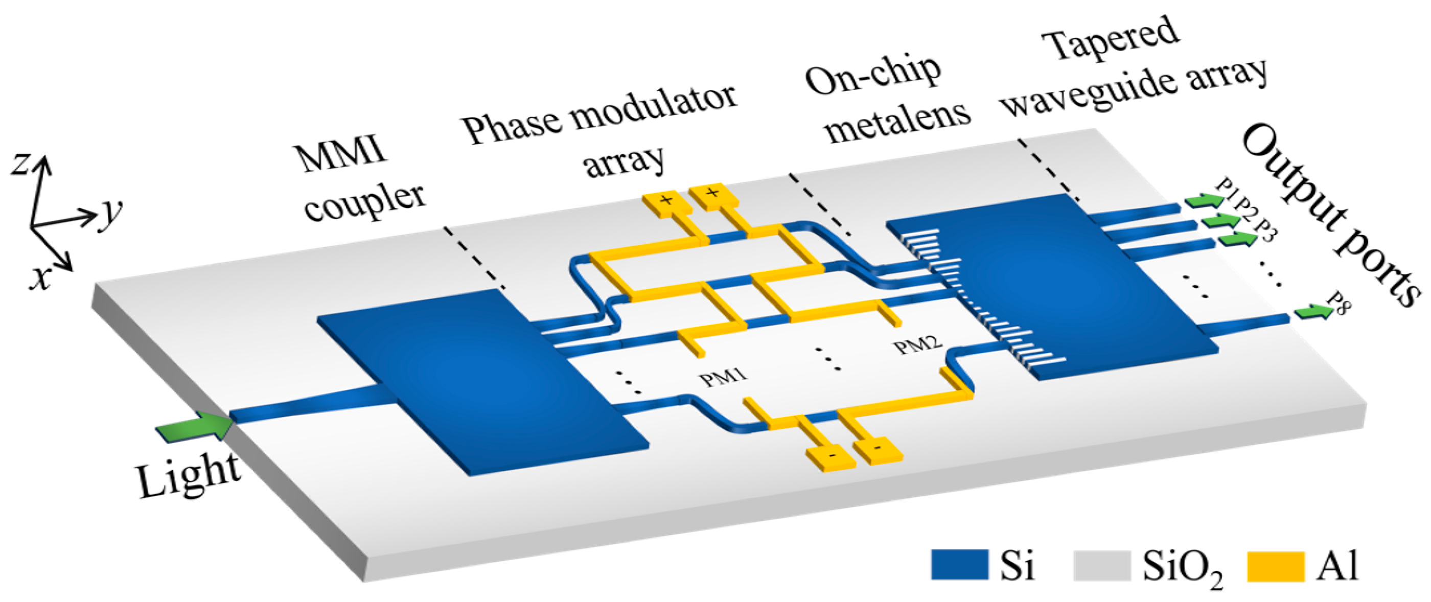
2.1. Configuration of the Proposed Optical Switch

Figure 1 delineates the configuration of the proposed integrated optical switch, comprising a spot size converter (SSC), an input MMI coupler, a phase modulator (PM) array, a beam-transformation region with an on-chip metalens layer, and a tapered waveguide array serving as the output ports. Incident light from a tunable laser is injected into the chip through the SSC and subsequently evenly divided into multiple channels via a 1 × N MMI coupler. The phases of the propagating modes among the multiple channels are meticulously managed utilizing the PM, which is activated by a strategically positioned heater above the waveguides. A single applied voltage facilitates the phase modulation across distinct waveguides, featuring metal strips with a length difference ΔL on each waveguide. Within the PM array, two centrosymmetric metal strips, PM1 and PM2, are configured with identical parameters, enabling control over beam deflection in both negative and positive directions. Subsequently, the guided mode, characterized by a specific phase difference (Δφ) between adjacent waveguide channels, couples to the beam-transformation region. Here, the on-chip metalens layer, comprising an array of slots with varying widths and lengths, manipulates the wavefront and performs a fast Fourier transform, thereby facilitating beam deflection at varying power levels. The output-tapered waveguide array, designed with a tilt angle aligned with each deflected beam, captures output beams with minimal optical loss. Ultimately, this configuration effectively accomplishes beam switching between multiple output ports as the applied power is gradually increased, supported by the metalens. The suggested optical switch is implemented on a silicon-on-insulator (SOI) platform [11,12,13,14,15]. The silicon (Si) waveguide features a core thickness of 220 nm, encapsulated by a 3 µm thick silica (SiO2) buried oxide (BOX) layer and a 2 µm thick SiO2 upper cladding layer. An aluminum (Al) alloy heater, positioned atop the waveguide, facilitates waveguide heating.

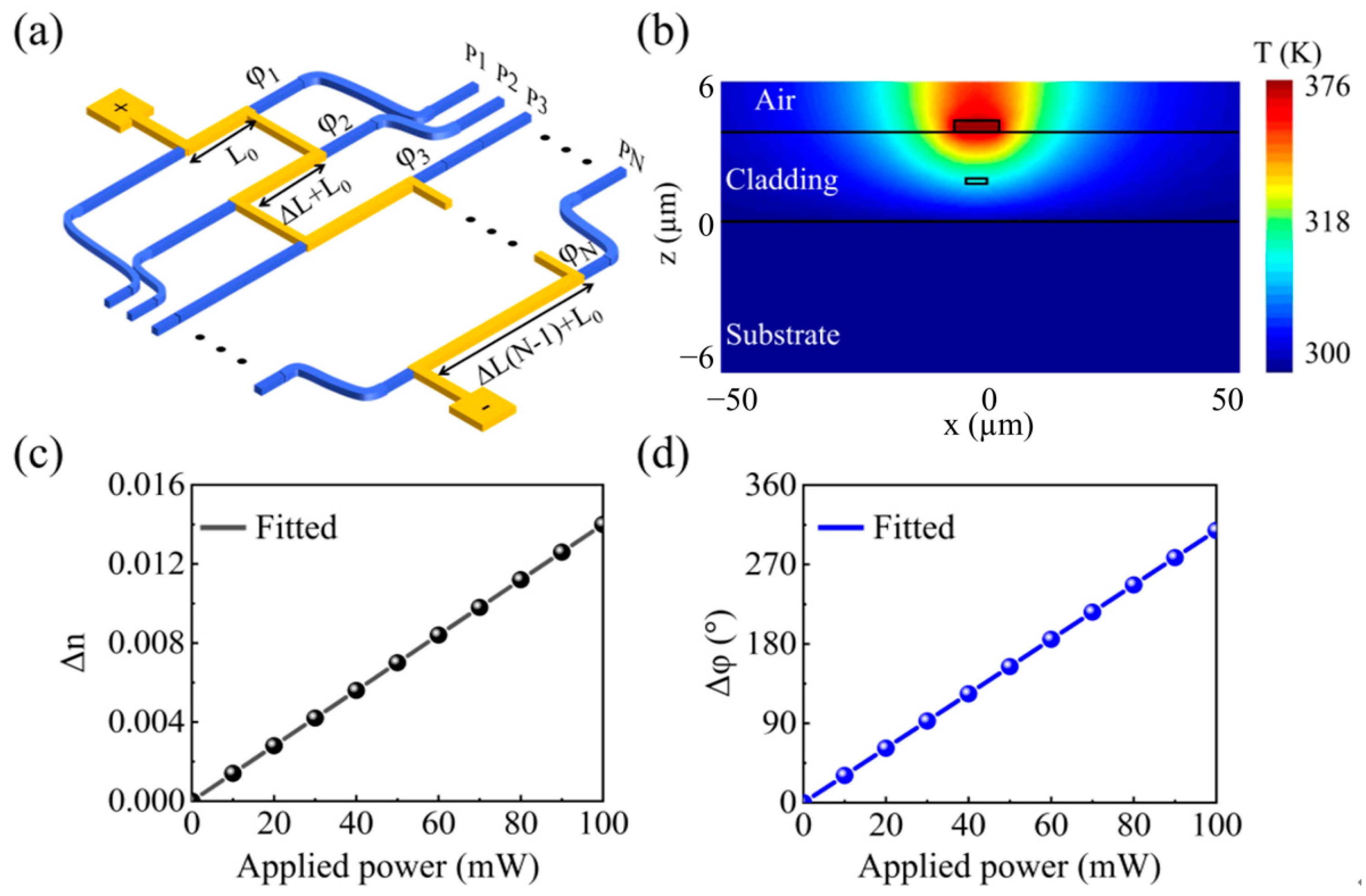
2.2. Design of the Phase Modulator Array

To examine the switching response of the proposed optical switch incorporating an on-chip metalens, the design and modulation characteristics of a PM array were first inspected. The incident beam is evenly split into 16 channels firstly by a designed input MMI coupler, with the phases of the propagating modes controlled by the PM array. Detailed parameters and beam-splitting performance are addressed in Appendix A. The configuration of the PM array is illustrated in Figure 2a, which shows that the heater is strategically positioned above the waveguides to induce the requisite phase shifts. A single applied voltage controls the phase of distinct waveguides, each featuring metal strips with a 60 µm length difference (ΔL). The effective refractive index difference (Δn) in the Si waveguide cross-section increases progressively with escalating voltage, calculated as Δ n = Δ T · n / T , where ∂n/∂T represents the thermal coefficient of Si (1.84 × 10⁻⁴/K) and ΔT represents the temperature change in the Si core [7]. Thermal simulations of the phase modulator were conducted using a commercial software program, Ansys/Lumerical 2023 R2. Initially, the cross-sectional structure of the device and the material properties, including the thermal and electrical conductivity, were defined within the HEAT solver. Simulation sweeps were subsequently performed by applying specified power values in incremental steps to obtain cross-sectional temperature distributions, which were saved for each parameter set. To derive the relationship between the effective refractive index change and temperature variation, the finite difference eigenmode (FDE) solver provided by Ansys/Lumerical was employed. The saved temperature map data were imported via the temperature grid property, enabling the FDE solver to compute the effective refractive index of the silicon waveguide across varying temperature profiles. This analysis facilitated the determination of phase modulation in response to the applied electrical power. Figure 2b displays the temperature distribution for the thermo-optic modulator at an applied electrical power of 100 mW, showcasing a substantial thermal effect on the Si waveguide. The temperature of the Si core escalates with rising applied power, leading to a modification in the effective refractive index. Variations in the applied power correspond directly to alterations in the temperature distribution. The temperature map corresponding to the applied electrical power of 100 mW is presented as a representative example to demonstrate the influence of the thermo-optic effect. A minimum heater length (L0) of 80 μm is determined to be necessary for achieving a π-phase shift with a temperature change ΔT. The relationship between the simulated Δn and the driving power is depicted in Figure 2c. The results show that Δn increases linearly correlating with an increase in applied power, resulting in a slope of 0.00014. The relationship between Δφ and the applied power of the multiple channels was checked, as shown in Figure 2d. The Δφ between adjacent waveguide channels, determined by the heater length difference, is expressed as Δ φ   = 2 π n eff Δ L / λ , where neff, ΔL, and λ stand for the effective refractive index of the guided mode of the waveguide, the length difference of the heaters, and the wavelength of interest, respectively [12]. It is indicated that neff increases linearly with the applied electrical power, as depicted in Figure 2c, implying that Δφ increases linearly with the applied power. Overall, the phases of propagating modes among the multiple channels can be precisely controlled utilizing a single PM, which is induced by a strategically positioned heater above the waveguides, thereby enabling efficient phase control and beam deflection. To estimate the response time of the optical switch, a finite element method (FEM) heat transfer simulation was conducted to examine the transient thermal response. The rise and fall times of the temperature change in the core of the waveguide were found to be approximately 143 μs, equivalent to the response speed of the optical switch.

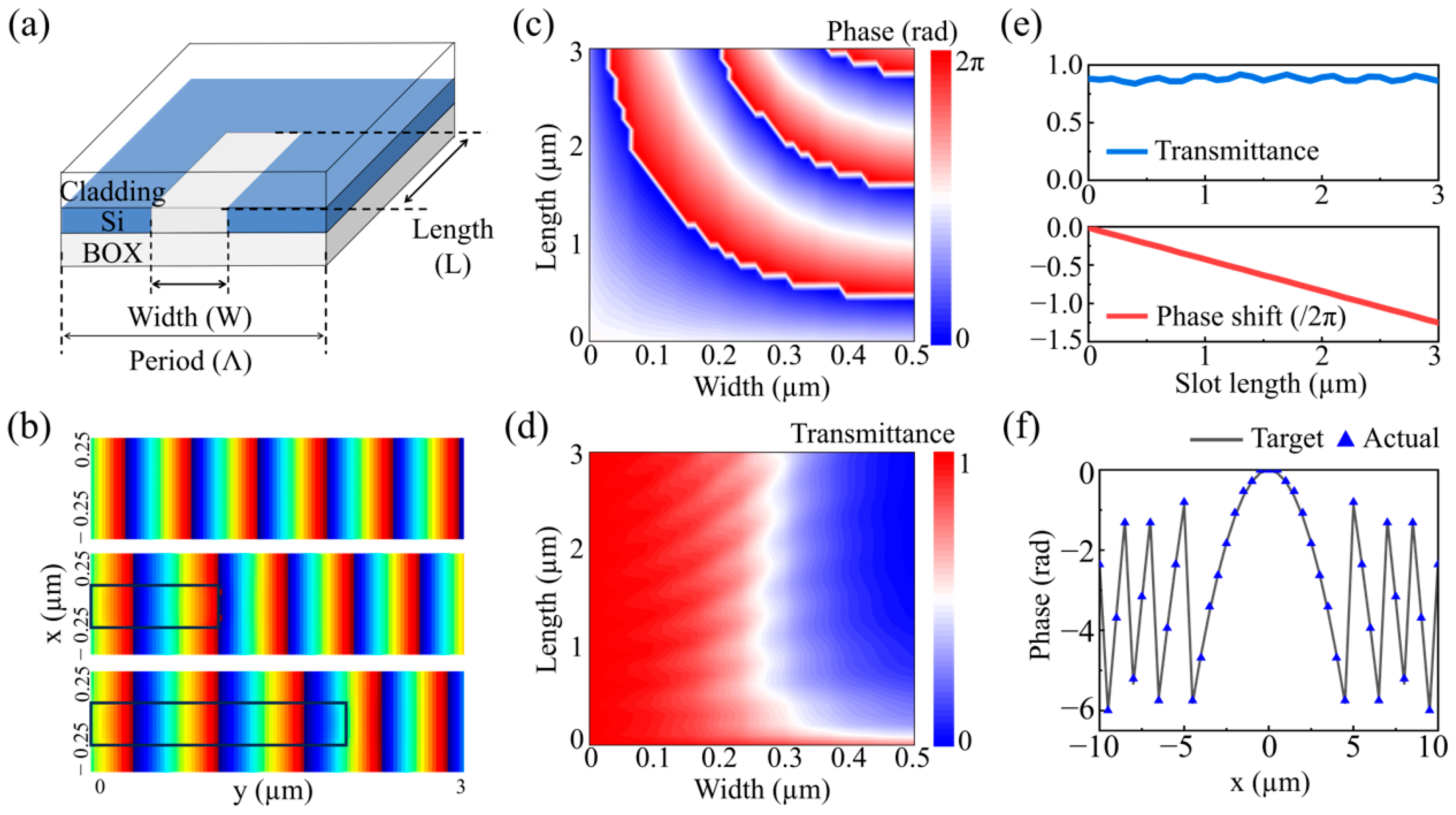
2.3. Design of On-Chip Metalens

On-chip metalens, designed to perform a fast Fourier transform (FFT), was theoretically formulated and validated through three-dimensional (3D) finite-difference time-domain (FDTD) simulations (Ansys/Lumerical Inc., Canada). A perfectly matched layer (PML) was used as boundary conditions, while a fundamental transverse electric (TE) mode was used as the excitation light source. The metalens employed an array of slots with varying widths and lengths along the x-direction to manipulate the phases of the propagating modes originating from the phase modulator array. Figure 3a shows a schematic of the designed unit cell, where W, L, and Λ indicate the slot width, slot length, and the unit cell period, respectively. Optical mode profiles of the transmitted TE waves through the slot units are depicted in Figure 3b. Here, the electric-field distributions for different configurations are shown for the cases of L = 0 µm, W = 0 µm; L = 1 µm, W = 0.14 µm; and L = 2 µm, W = 0.14 µm. As anticipated, the phase shift unequivocally correlates with the dimensions of the slot, influenced by the wavenumber differences between the slot and the surrounding slab waveguides. It is noted that the variation in slot dimensions alters the effective refractive index of the unit structure. By meticulously controlling the slot width and length, the phase delay imparted to incident light waves can be finely adjusted, thereby shaping the light wavefront [25]. The period of the unit cell was consistently maintained at 500 nm, which is less than half the wavelength, ensuring effective phase manipulation [27]. Phase shift and transmission characteristics were systematically studied by varying W from 0 to 0.5 μm and L from 0 to 3 μm, as shown in Figure 3c,d. For initial demonstrations, the slot unit cell maintained a constant width of W = 0.14 μm, which facilitated a phase shift ranging from 0 to 2π by varying the slot length from 0 to 3 μm, and simultaneously achieving a high transmission efficiency exceeding 0.86, as shown in Figure 3e. The target phase shifts required for the initial FFT lens were determined using Equation (1) [23] as follows:
φ M L x = 2 π λ · n e f f _ s l a b f f 2 + x 2 ,
where φ M L , n e f f _ s l a b , and f denote the required phase shifts of the metalens layer, the effective refractive index of the slab-guided mode, and the focusing length, respectively. Here, n e f f _ s l a b is calculated to be 2.93 at a wavelength of 1550 nm, reflecting the properties of the SiO2 cladding and Si core combination. It has been established that a silicon waveguide exhibits extremely low absorption loss and minimal dispersion around 1550 nm wavelength, rendering efficient light transmission. Furthermore, the utilization of this specific wavelength minimizes the nonlinear effect in silicon, thereby fortifying the stability and fidelity of signal transmission [10,16]. A comparison between the target and the actual phase profiles of the metalens is depicted in Figure 3f. The theoretical predictions of the phase profiles, calculated for a focal length of 20 µm based on Equation (1), are represented by solid black lines. Simultaneously, the actual phase distribution, determined by the unit cell parameters, is depicted by blue triangular patterns, closely matching the theoretical predictions.

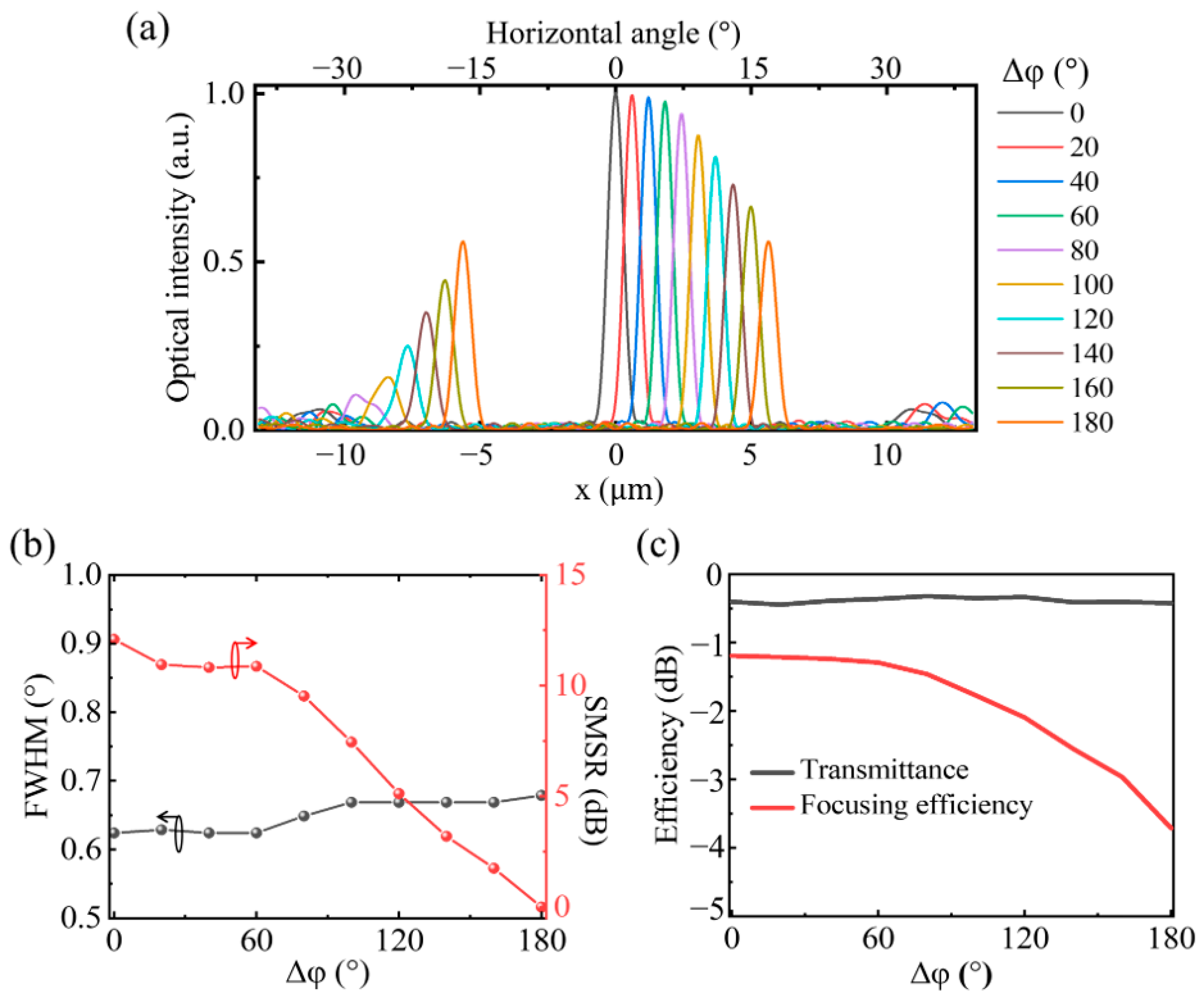
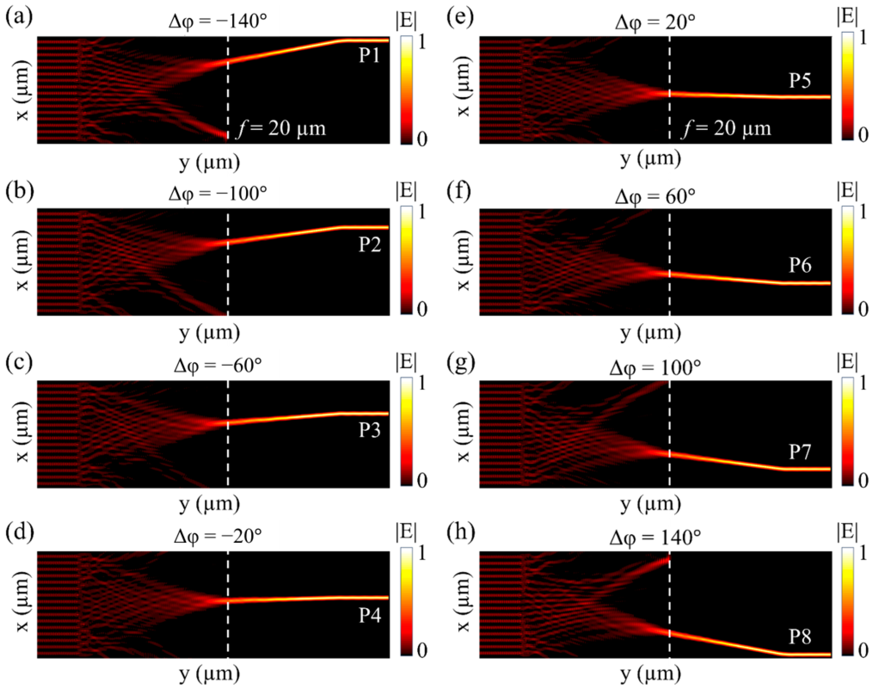
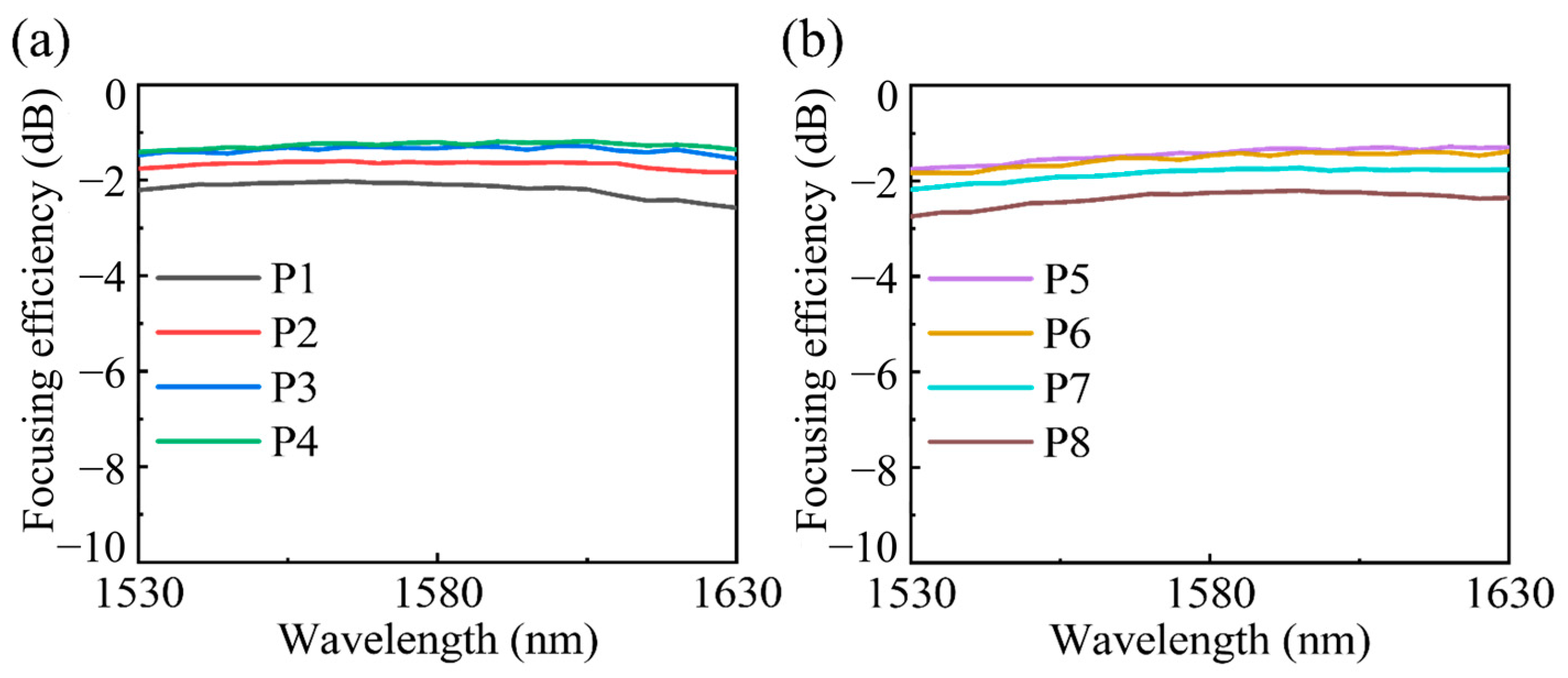
3. Results and Discussion

Beam shaping and deflection in the beam-transformation region are governed by the principles of OPA theory, enabling beam scanning through the introduction of variable phase gradients across multiple input channels. The integration of the on-chip metalens layer into this region effectively manipulates the wavefront. The designed metalens facilitates fast Fourier transform operations, analogous to the frequency domain analysis described by the Fraunhofer diffraction principle in optics. This capability enables the generation of far-field patterns exhibiting various deflection angles at the focal plane of metalens. For a uniform waveguide array, the scanning angle Ψ is determined by the applied phase difference, according to the formula sin Ψ = λ Δ φ / ( 2 π Λ ch ) , where Δφ and Λch represent the phase difference and channel spacing, respectively [13]. To further evaluate the emission response of the proposed optical switch, the number of channels and the channel spacing were set to 16 and 1.1 µm, respectively, by scrutinizing the beamwidth and focusing efficiency. The metalens-assisted optical switch ultimately achieved beam switching with a footprint of approximately 1.1 mm × 0.8 mm, including the input MMI coupler, PM array, and beam-transformation region. The functionality of the on-chip metalens was validated through meticulous simulations. Figure 4 reveals the simulated propagating beam profiles and the corresponding electric-field profiles in the focusing plane, varying the phase difference from 0° to 180° in increments of 20°. The beam deflection in multiple directions is governed by the Fraunhofer diffraction and light interference for the OPA system. The precise phase control of each emitter unit, facilitated by the PM array, enables the management of both the propagation direction and interference characteristics of the emitted beam. The designed metalens serves as a device that carries out optical Fourier transform operations related to Fraunhofer diffraction [21]. A far-field pattern in relation to a deflection angle can thus be generated at the focal plane of the metalens. Figure 4a exhibits the propagating profile at a scanning angle of 0°, corresponding to a Δφ of 0°. As Δφ increases, the deflection angle of the incident beam also increases, resulting in the appearance of two identical beams at Δφ of ±π, as shown in Figure 4j. Figure 5a illustrates the horizontal cross-sections of the focusing plane for Δφ ranging from 0° to 180°. As Δφ increases, the beam scans in the positive x-direction, providing a horizontal scanning region of approximately 17° in the slab waveguide. The positions of the grating lobes are determined by sin Ψ grating = ± n λ / Λ ch for the uniform OPA, where n signifies the order of the grating lobes. Notably, no grating lobes are observed at Δφ = 0. It is important to note that during beam scanning, the main lobe intensity declines while the grating lobe intensity increases within the far-field diffraction envelope, a phenomenon determined by a single antenna element. The main lobe intensity performance was characterized through the side-mode suppression ratio (SMSR), defined as log10(Imain_max/Igrating_max). In addition, the full width at half maximum (FWHM) was thoroughly investigated as a crucial factor affecting beam-switching accuracy. Both the SMSR and FWHM related to the focused beam were analyzed concerning variable phase differences, as shown in Figure 5b. The FWHM beamwidth is determined by the entire span of the array, equivalent to Nch·Λch, where Nch represents the number of waveguides. The SMSR decreases from 12.1 dB to 0 dB as Δφ increases from 0 to 180°, with a stable beamwidth of approximately 0.62 µm. The transmittance and focusing efficiency of the proposed optical switch were characterized in detail, as illustrated in Figure 5c. During beam scanning, the transmission efficiency of the metalens maintains a high value of approximately −0.4 dB. Simultaneously, the focusing efficiency decreases from −1.2 dB to −3.6 dB, attributed to the gradually increasing grating lobes. Consequently, the designed optical switch yielded a total insertion loss (IL) of approximately 2.6 dB, primarily attributable to losses in the input MMI coupler, light propagation, and on-chip metalens. It is implied that the metalens-assisted optical switch can achieve efficient beam deflection with variable phase differences across multiple channels.
The output ports were meticulously designed with a focus on maximizing coupling efficiency and minimizing the overall footprint. The output-tapered waveguide array is designed to align with the deflection angle of each beam, ensuring that the output beams are captured entirely with minimal optical loss. The specifications of the taper length, width, and radius of the connecting arc bend were set at 10 µm, 1.2 µm, and 30 µm, respectively, to achieve optimal coupling efficiency. The integral switching characteristics of the system were thoroughly simulated and analyzed. The propagating field profiles along the xy direction, facilitated by the specifically designed output ports, are presented in Figure 6. This visualization demonstrates the 1 × 8 beam-switching capability as the beam transitions from Port 1 (P1) to Port 8 (P8) based on variable phase differences. It is crucial to ensure that the focused beams between the adjacent output ports do not overlap to ensure high-efficiency optical path switching. The deflection angle of the incident beam increases with the increasing Δφ values. The respective phase differences for efficient 1 × 8 beam switching were set at ±20°, ±60°, ±100°, and ±140°, accommodating the directional requirements of each output port. For the designed on-chip metalens, wavefront manipulation can be fulfilled through gap slots of varying widths and lengths, ensuring minimal insertion loss, high tolerance to manufacturing variations, and compatibility with the current CMOS process standards. Comprehensive details on the specific process of metalens fabrication are provided in Appendix B. To the best of our knowledge, the proposed device constitutes a pioneering instrument that integrates an OPA and on-chip metalens, enabling compact and scalable multi-path beam switching.
The corresponding horizontal cross-sections of eight ports are illustrated in Figure 7a. As mentioned before, the main lobe intensity shifts gradually across the far-field diffraction envelope during the beam scanning process, with a simulated intensity variation of approximately 1.2 dB. It is essential to ensure that the main lobes of the eight outgoing beams are sufficiently separated to prevent optical crosstalk between adjacent channels, thereby limiting the number of output ports. The designed taper width of 1.2 µm and the intervening gap of 0.2 µm were chosen to comply with CMOS fabrication standards. Figure 7b shows the observed coupling efficiency for each output port, achieving the efficiency variation from −1.4 dB to −2.6 dB as the beam is directed from P1 to P8. It is hence demonstrated that the proposed device enables efficient 1 × 8 beam switching within a compact footprint. The metalens-assisted optical switch ultimately achieves beam switching by adjusting a single applied power, which modulates the phase of distinct waveguides through metal strips with a length difference of ΔL. Beam switching from P1 to P8 corresponds to required power consumption levels of 45.3, 32.4, 19.5, 6.51, 6.51, 19.5, 32.4, and 45.3 mW, respectively, as shown in Figure 7b.
The spectral characterization of the proposed metalens-assisted optical switch was simulated and analyzed over a spectral regime spanning λ = 1530–1630 nm, covering both C and L bands, as shown in Figure 8. The simulated focusing efficiency is as high as −1.20 dB at 1550 nm and beyond −1.41 dB in the whole spectral range for Port 4. Additionally, the focusing efficiency varies from −2.03 dB to −2.57 dB for Port 1, as presented in Figure 8a, underpinning a highly efficient broadband performance. Table 1 presents a performance comparison of multichannel optical switches based on devices including an MMI-MZI, ring resonator, Y-branch, and sub-wavelength grating (SWG) in terms of the number of output ports (Nout), integrated footprint, insertion loss (IL), and power consumption. Conventional optical switches suffer from drawbacks including a relatively large footprint and limited number of output ports. While SWG-assisted optical switches offer a reduced footprint, their high IL and power consumption hinder their suitability for large-scale photonic integrated circuits. In contrast, the proposed device achieves efficient beam deflection, rendering 1 × 8 beam switching under a compact footprint, with a lower IL and power consumption of 2.6 dB and 45.3 mW, respectively. The planned experimental procedure for the suggested optical switch is addressed in Appendix C.
Considering that the channel spacing (Λch) of the PM array and the focusing length (f) of designed FFT metalens can directly affect the beam-switching characteristics, the suggested optical switch could be meticulously designed to tailor the focusing beamwidth and deflection angle, ultimately varying the numbers of output ports. Several devices with different OPAs and metalens configurations were simultaneously characterized, as presented in Table 2. Here, FW, x_max, and Nout represent the full beam width, maximum deflection position with the Δφ of π, and the maximum number of achievable switching paths, respectively. As previously mentioned, the gap between adjacent output tapers was set as 0.2 µm to meet CMOS fabrication standards. Additionally, Nout is the integer closest to x_max/0.5(FW + 0.2). The value of Nout was observed to increase with Nch, exhibiting numbers of 5, 8, and 16 for the PM array corresponding to Nch = 8, 16, and 32, respectively, with a fixed f of 20 µm. The FWHM and FW of the focused beam decreases with the f decreases; however, the value of x_max becomes smaller simultaneously, resulting in an insignificant fluctuation in terms of the Nout. The results of integrated optical switches in different configurations show potential for its scalability. The capability of efficient 1 × N beam switching with a compact design and scalability underscores the potential of metalens-assisted optical switches and is anticipated to be a promising strategy for managing complex on-chip optical networks.

4. Conclusions

An integrated optical switch featuring an on-chip metalens was successfully demonstrated, enabling scalable and efficient beam switching across multiple ports within a compact footprint. The thermo-optic phase modulator array was designed to control multiple phases with a single applied voltage by using heaters with gradually increasing lengths, streamlining operation. The propagating mode, characterized by specific phase differences between adjacent waveguide channels, is directed to the beam-transformation region. The on-chip metalens layer, which utilizes an array of slots with varying lengths, was integrated into the beam-transformation region to manipulate the wavefront and perform an FFT function, thereby achieving effective beam deflection with variable angles under distinct applied power levels. The output-tapered waveguide array, designed with a tilt angle matching the angle of each deflected beam, captured the output beams with minimal optical loss. Ultimately, the proposed optical switch achieved efficient 1 × 8 beam switching with variable applied powers at a wavelength of 1550 nm. The integration of different OPAs and metalenses demonstrated potential scalability by enabling path switching ranging from 4 to 16, representing a significant advancement in scalable beam switching for large-scale optical networks. The proposed scheme might exhibit limitations in accommodating larger channel output ports and achieving compactness, predominantly constrained by the focused spot size and the beam steering range. Future research could be dedicated to investigating an aperiodic OPA configuration to mitigate the limitation in steering angle. Simultaneously, increasing the number of channels and reducing the focal length holds promise for narrowing the focused beam width and thereby enhancing the efficiency and scalability of beam switching.

Author Contributions

Simulation and design, C.W.; investigation, C.W.; writing—original draft preparation, C.W.; writing—review and editing, C.W., H.L., J.L., and S.-S.L. All authors have read and agreed to the published version of the manuscript.

Funding

This research was supported by the Core Research Institute Basic Science Research Program through the National Research Foundation of Korea (NRF) funded by the Ministry of Education (No. 2018R1A6A1A03025242) and the research grant of Kwangwoon University in 2024.

Institutional Review Board Statement

Not applicable.

Informed Consent Statement

Not applicable.

Data Availability Statement

Data are contained within the article.

Conflicts of Interest

The authors have no conflicts of interest to declare.

Appendix A

The suggested input 1 × 16 MMI coupler was meticulously analyzed and optimized using a simulation tool based on the beam propagation method (BeamPROP; Synopsys Inc., Sunnyvale, CA, USA). Figure A1a displays the electric-field profile of the MMI coupler, demonstrating that incident light is evenly split into 16 channels. The coupling efficiencies of the output ports are presented in Figure A1b, highlighting that the designed MMI coupler achieves superior performance with a stable coupling efficiency of approximately −12.1 dB. The width of the MMI region was fixed at 24 µm, while the corresponding length was optimized to 65.5 µm to ensure effective light distribution. The taper widths of the input (Wi) and output ports (Wo), the taper length (Ltaper), and the spacing between the two output ports (Λtaper) were properly determined to optimize performance. The specific design parameters are presented in Table A1.
Figure A1. (a) Simulated electric-field profiles of 1 × 16 MMI coupler at a wavelength of 1550 nm; (b) corresponding coupling efficiencies of each port.
Photonics 11 00611 g0a1
Table A1. Structural parameters of designed 1 × 16 MMI coupler.
WMMILMMIWiWoLtaperΛtaper
24 µm65.5 µm2.0 µm1.3 µm10 µm1.51 µm

Appendix B

The designed on-chip metalens could be fabricated following the standard CMOS process, as illustrated in detail in Figure A2. Initially, a buried oxide SiO2 layer and a Si core layer can be sequentially deposited on the Si substrate using plasma-enhanced chemical vapor deposition (PECVD). The Si waveguide pattern can then be defined on the thin film via photolithography. Subsequently, the Si layer can be fully etched, followed by the removal of the photoresist (PR) layer. Finally, the upper cladding layer can be deposited onto the patterned silicon waveguide using the PECVD method [27].
Figure A2. Schematic of the fabrication procedure for the proposed on-chip metalens.
Photonics 11 00611 g0a2

Appendix C

The designed optical switch could be experimentally characterized considering three primary aspects: insertion loss, modulation speed, and power consumption. Initially, the incident light generated by a tunable laser passes through a polarization controller, an erbium-doped fiber amplifier (EDFA), and then coupled to the fabricated chip via an edge coupler. To quantify the insertion loss, the light transmitted through the fabricated optical switch exits through individual output ports and is subsequently re-coupled into the output fiber. Optical power measurements at each output port are performed using an optical power meter to determine the total insertion loss. For evaluating the modulation performance of the optical switch, an MZI structure is utilized with a heater integrated into one arm to induce a phase difference between its two channels. A low-frequency sawtooth voltage waveform is generated by an arbitrary waveform generator and applied to the heater electrode via the probes. The optical output is converted into an electrical signal using a photodetector connected to an oscilloscope. By analyzing the optical output waveform on the oscilloscope, the rise and fall times of the light intensity are determined to characterize the modulation speed of the optical switch. Typically, the power consumption of an optical switch is quantified by the power necessary to achieve a phase shift of π. During the experiment, the input voltage gradually increases until the power emitted from the MZI approaches zero, signaling an approaching phase shift of π between its two arms.
It is worth noting that the thermo-optic phase modulator is susceptible to environmental temperature variations, highlighting the importance of implementing a temperature compensation mechanism in the experiment to ensure the consistent performance of the optical switch. Initially, real-time temperature sensors will monitor temperature fluctuations in both the optical thermo-optic modulator and its environment. A comprehensive analysis and detailed testing of the performance across varying temperatures will be conducted, encompassing key parameter measurements, including optical transmission loss, phase modulation capability, and electro-optic efficiency. The precise temperature-dependent model of the performance will be established based on the collected data. A feedback mechanism could regulate the operational temperature of the optical device to maintain stability within the desired range. Subsequently, algorithms will be developed to compensate for performance variations based on insights from the temperature dependency model and performance analysis. These algorithms will autonomously adjust the thermo-optic modulator’s control parameters in response to real-time temperature data, effectively mitigating the adverse effects of temperature fluctuations on the performance of the thermo-optic phase modulator.

References

  1. Wang, K.; Dong, X.; Köhler, M.H.; Kienle, P.; Bian, Q.; Jakobi, M.; Koch, A.W. Advances in optical fiber sensors based on multimode interference (MMI): A review. IEEE Sens. J. 2020, 21, 132–142. [Google Scholar] [CrossRef]
  2. Chen, L.; Chen, Y.K. Compact, low-loss and low-power 8 × 8 broadband silicon optical switch. Opt. Express 2012, 20, 18977–18985. [Google Scholar] [CrossRef] [PubMed]
  3. Duan, F.; Chen, K.; Chen, D.; Yu, Y. Low-power and high-speed 2 × 2 thermo-optic MMI-MZI switch with suspended phase arms and heater-on-slab structure. Opt. Lett. 2021, 46, 234–237. [Google Scholar] [CrossRef] [PubMed]
  4. Gao, Y.; Sun, X.; Li, P.; Zhang, D. Polymer mode selecting switch based on cascaded MMI couplers. IEEE Photonics Technol. Lett. 2021, 33, 147–150. [Google Scholar] [CrossRef]
  5. Cheng, R.; Zhang, D.; Wang, J.; Wang, C.; Gao, F.; Sun, X.; Shi, Z.; Cui, Z.; Chen, C. Fluorinated photopolymer cascaded MMI-based integrated optical waveguide switching matrix with encoding functions. Opt. Express 2019, 27, 12883–12898. [Google Scholar] [CrossRef] [PubMed]
  6. Lu, L.; Zhou, L.; Li, Z.; Li, D.; Zhao, S.; Li, X.; Chen, J. 4 × 4 silicon optical switches based on double-ring-assisted Mach–Zehnder interferometers. IEEE Photonics Technol. Lett. 2015, 27, 2457–2460. [Google Scholar] [CrossRef]
  7. Han, Y.T.; Shin, J.U.; Park, S.H.; Han, S.P.; Baek, Y.; Lee, C.H.; Noh, Y.O.; Lee, H.J.; Park, H.H. Fabrication of 10-channel polymer thermo-optic digital optical switch array. IEEE Photonics Technol. Lett. 2009, 21, 1556–1558. [Google Scholar] [CrossRef]
  8. Watts, M.R.; Sun, J.; DeRose, C.; Trotter, D.C.; Young, R.W.; Nielson, G.N. Adiabatic thermo-optic Mach–Zehnder switch. Opt. Lett. 2013, 38, 733–735. [Google Scholar] [CrossRef]
  9. Lian, T.; Xie, Y.; Yu, Q.; Sun, S.; Sun, X.; Wang, X.; Zhang, D. Mode-independent optical switch based on graphene-polymer hybrid waveguides. Photonics 2023, 10, 1372. [Google Scholar] [CrossRef]
  10. Zhou, J.; Gallion, P. Operation principles for optical switches based on two multimode interference couplers. J. Lightw. Technol. 2011, 30, 15–21. [Google Scholar] [CrossRef]
  11. Brunetti, G.; Marocco, G.; Di Benedetto, A.; Giorgio, A.; Armenise, M.N.; Ciminelli, C. Design of a large bandwidth 2 × 2 interferometric switching cell based on a sub-wavelength grating. J. Opt. 2021, 23, 085801. [Google Scholar] [CrossRef]
  12. Gobet, M.; Herbst, P.; Baroni, P.; Marxer, C. Applications of optical MEMS for space missions. In Proceedings of the 6th ESA Round Table on Micro/Nano Technologies for Space, Noordwijk, The Netherlands, 8–12 October 2007; pp. 13–17. Available online: https://escies.org/webdocument/showArticle?id=766&groupid=6 (accessed on 1 June 2024).
  13. Chung, S.; Abediasl, H.; Hashemi, H. A monolithically integrated large-scale optical phased array in silicon-on-insulator CMOS. IEEE J. Solid-State Circuits 2018, 53, 275–296. [Google Scholar] [CrossRef]
  14. Im, C.-S.; Kim, S.-M.; Lee, K.-P.; Ju, S.-H.; Hong, J.-H.; Yoon, S.-W.; Kim, T.; Lee, E.-S.; Bhandari, B.; Zhou, C.; et al. Hybrid integrated silicon nitride–polymer optical phased array for efficient light detection and ranging. J. Lightw. Technol. 2021, 39, 4402–4409. [Google Scholar] [CrossRef]
  15. Bhandari, B.; Wang, C.; Gwon, J.-Y.; Heo, J.-M.; Ko, S.-Y.; Oh, M.-C.; Lee, S.-S. Dispersive silicon–nitride optical phased array incorporating arrayed waveguide delay lines for passive line beam scanning. Sci. Rep. 2022, 12, 18759. [Google Scholar] [CrossRef] [PubMed]
  16. Wang, P.; Luo, G.; Xu, Y.; Li, Y.; Su, Y.; Ma, J.; Wang, R.; Yang, Z.; Zhou, X.; Zhang, Y.; et al. Design and fabrication of a SiN-Si dual-layer optical phased array chip. Photonics Res. 2020, 8, 912–919. [Google Scholar] [CrossRef]
  17. Kim, Y.; Yoon, H.; You, J.-B.; Kim, M.; Park, H.-H. Wide-angle beam-steering using an optical phased array with non-uniform-width waveguide radiators. Photonics 2020, 7, 56. [Google Scholar] [CrossRef]
  18. Im, C.-S.; Bhandari, B.; Lee, K.-P.; Kim, S.-M.; Oh, M.-C.; Lee, S.-S. Silicon nitride optical phased array based on a grating antenna enabling wavelength-tuned beam steering. Opt. Express 2020, 28, 3270–3279. [Google Scholar] [CrossRef] [PubMed]
  19. Hutchison, D.N.; Sun, J.; Doylend, J.K.; Kumar, R.; Heck, J.; Kim, W.; Phare, C.T.; Feshali, A.; Rong, H. High-resolution aliasing-free optical beam steering. Optica 2016, 3, 887–890. [Google Scholar] [CrossRef]
  20. Shin, M.C.; Mohanty, A.; Watson, K.; Bhatt, G.R.; Phare, C.T.; Miller, S.A.; Zadka, M.; Lee, B.S.; Ji, X.; Datta, I.; et al. Chip-scale blue light phased array. Opt. Lett. 2020, 45, 1934–1937. [Google Scholar] [CrossRef]
  21. Dostart, N.; Zhang, B.; Khilo, A.; Brand, M.; Al Qubaisi, K.; Onural, D.; Feldkhun, D.; Wagner, K.H.; Popović, M.A. Serpentine optical phased arrays for scalable integrated photonic lidar beam steering. Optica 2020, 7, 726–733. [Google Scholar] [CrossRef]
  22. Alemany, R.; Muñoz, P.; Pastor, D.; Domínguez, C. Thermo-optic phase tuners analysis and design for process modules on a silicon nitride platform. Photonics 2021, 8, 496. [Google Scholar] [CrossRef]
  23. Heck, M.J. Highly integrated optical phased arrays: Photonic integrated circuits for optical beam shaping and beam steering. Nanophotonics 2017, 6, 93–107. [Google Scholar] [CrossRef]
  24. Chen, S.; Huang, J.; Yin, S.; Milosevic, M.M.; Pi, H.; Yan, J.; Chong, H.M.H.; Fang, X. Metasurfaces integrated with a single-mode waveguide array for off-chip wavefront shaping. Opt. Express 2023, 31, 15876–15887. [Google Scholar] [CrossRef]
  25. Li, H.; Lee, W.-B.; Zhou, C.; Choi, D.-Y.; Lee, S.-S. Flat retroreflector based on a metasurface doublet enabling reliable and angle-tolerant free-space optical link. Adv. Opt. Mater. 2021, 9, 2100796. [Google Scholar] [CrossRef]
  26. Chen, C.; Qi, W.; Yu, Y.; Zhang, X. On-chip optical spatial-domain integrator based on Fourier optics and metasurface. Nanophotonics 2021, 10, 2481–2486. [Google Scholar] [CrossRef]
  27. Wang, Z.; Li, T.; Soman, A.; Mao, D.; Kananen, T.; Gu, T. On-chip wavefront shaping with dielectric metasurface. Nat. Commun. 2019, 10, 3547. [Google Scholar] [CrossRef] [PubMed]
  28. Rajabalipanah, H.; Abdolali, A.; Iqbal, S.; Zhang, L.; Cui, T.J. Analog signal processing through space-time digital metasurfaces. Nanophotonics 2011, 10, 1753–1764. [Google Scholar] [CrossRef]
  29. Yang, R.; Shi, Y.; Dai, C.; Wan, C.; Wan, S.; Li, Z. On-chip metalenses based on one-dimensional gradient trench in the broadband visible. Opt. Lett. 2020, 45, 5640–5643. [Google Scholar] [CrossRef]
  30. Alquliah, A.; Elkabbash, M.; Cheng, J.; Verma, G.; Saraj, C.S.; Li, W.; Guo, C. Reconfigurable metasurface-based 1 × 2 waveguide switch. Photonics Res. 2021, 9, 2104–2115. [Google Scholar] [CrossRef]
  31. Li, H.; Zhou, C.; Lee, W.-B.; Choi, D.Y.; Lee, S.-S. Flat telescope based on an all-dielectric metasurface doublet enabling polarization-controllable enhanced beam steering. Nanophotonics 2022, 11, 405–413. [Google Scholar] [CrossRef]
  32. Xie, Z.; Lei, T.; Li, F.; Qiu, H.; Zhang, Z.; Wang, H.; Min, C.; Du, L.; Li, Z.; Yuan, X. Ultra-broadband on-chip twisted light emitter for optical communications. Light Sci. Appl. 2018, 7, 18001. [Google Scholar] [CrossRef] [PubMed]
  33. Meng, Y.; Liu, Z.; Xie, Z.; Wang, R.; Qi, T.; Hu, F.; Kim, H.; Xiao, Q.; Fu, X.; Wu, Q.; et al. Versatile on-chip light coupling and (de) multiplexing from arbitrary polarizations to controlled waveguide modes using an integrated dielectric metasurface. Photonics Res. 2020, 8, 564–576. [Google Scholar] [CrossRef]
  34. Hsieh, P.Y.; Fang, S.L.; Lin, Y.S.; Huang, W.H.; Shieh, J.M.; Yu, P.; Chang, Y.C. Integrated metasurfaces on silicon photonics for emission shaping and holographic projection. Nanophotonics 2022, 11, 4687–4695. [Google Scholar] [CrossRef]
  35. Huang, Z.; Zheng, Y.; Li, J.; Cheng, Y.; Wang, J.; Zhou, Z.K.; Chen, L. High-resolution metalens imaging polarimetry. Nano Lett. 2023, 23, 10991–10997. [Google Scholar] [CrossRef]
  36. Li, J.; Liu, W.; Xu, H.; Huang, Z.; Wang, J.; Wen, J.; Yang, J.; Guan, J.; Wang, S.; Alù, A.; et al. An RGB-achromatic aplanatic metalens. Laser Photonics Rev. 2024, 18, 2300729. [Google Scholar] [CrossRef]
Figure 1. Configuration of the proposed compact metalens-assisted optical switch enabling efficient and scalable beam switching.
Photonics 11 00611 g001
Figure 2. (a) Schematic of designed phase modulator array; (b) temperature distribution map with an applied power of 100 mW; (c) correlation between Δn and applied power; (d) relationship between phase differences of multiple channels and applied power.
Photonics 11 00611 g002
Figure 3. (a) Schematic of a slot unit cell; (b) simulated electric-field distributions for different slot lengths. Simulated (c) phase and (d) transmittance profiles of the designed unit cell in terms of the slot width and length; (e) simulated transmittance and phase profile for a fixed slot width of 140 μm; (f) theoretical and actual phase profiles for a focusing length of 20 μm.
Photonics 11 00611 g003
Figure 4. Simulated propagating beam profiles and corresponding electric-field profiles in the focusing plane, with phase differences varying from (aj) 0 to 180° with increments of 20°.
Photonics 11 00611 g004
Figure 5. (a) Simulated horizontal cross-sectional beam patterns for Δφ ranging from 0° to 180°; (b) detailed analysis of FWHM and SMSR in terms of variable phase differences; (c) simulated transmittance and focusing efficiency of designed metalens with a focusing length of 20 µm.
Photonics 11 00611 g005
Figure 6. Simulated propagating beam profiles of 1 × 8 optical switch incorporating output ports for the Δφ of (a) −140°; (b) −100°; (c) −60°; (d) −20°; (e) 20°; (f) 60°; (g) 100°; (h) 140°.
Photonics 11 00611 g006
Figure 7. (a) Simulated horizontal cross-sectional beam patterns of 1 × 8 optical switch; (b) the focusing efficiency and required power consumption of each port.
Photonics 11 00611 g007
Figure 8. Focusing efficiencies when wavelengths vary from 1530 nm to 1630 nm for the (a) Port 1 to Port 4; (b) Port 5 to Port 8.
Photonics 11 00611 g008
Table 1. Comparison between the proposed device and conventional optical switches.
TypeNoutFootprintILPower ConsumptionReference
MMI-MZI88 × 8 mm24 dB70 mW[2]
Ring resonator43.4 × 1.6 mm2~5 dB22.37 mW[6]
Y-branch1015 × 8 mm21.35 dB50 mW[7]
SWG-assisted81.62 × 0.6 mm215 dB276 mW[11]
Metalens-assisted81.1 × 0.8 mm22.6 dB45.3 mWThis work
Table 2. Port numbers for beam switching in terms of Nch and f.
f
(µm)
Nch = 8Nch = 16Nch = 32
FWHM
(µm)
FW
(µm)
x_max
(µm)
NoutFWHM
(µm)
FW
(µm)
x_max
(µm)
NoutFWHM
(µm)
FW
(µm)
x_max
(µm)
Nout
100.741.544.950.420.874.990.230.524.914
201.382.477.250.621.107.280.420.757.216
302.314.9310.341.162.4510.380.771.6310.312
Disclaimer/Publisher’s Note: The statements, opinions and data contained in all publications are solely those of the individual author(s) and contributor(s) and not of MDPI and/or the editor(s). MDPI and/or the editor(s) disclaim responsibility for any injury to people or property resulting from any ideas, methods, instructions or products referred to in the content.

