Abstract
This study introduces the design of a nonlinear frequency-modulated continuous wave (FMCW) laser ranging system. In contrast to the commonly used triangular wave linear modulation, this study utilizes sinusoidal wave modulation. The frequency information of the original sinusoidal frequency-modulated signal is extracted using an on-chip interferometer based on SiON waveguides and IQ demodulation technology. After fitting the measured interference signal at equal frequency intervals, the corresponding distance information is derived using the fast Fourier transform (FFT). The principles underlying this method are thoroughly analyzed and derived, with its accuracy confirmed through experimental validation.
1. Introduction
There is an increasing demand for higher accuracy and resolution in target detection, particularly in fields such as military reconnaissance, aerospace, and autonomous driving [1,2]. Laser detection and ranging technology (LIDAR), which employs lasers as a medium, is progressively supplanting traditional ranging techniques due to its high resolution, accuracy, and strong anti-interference capabilities. In comparison to traditional pulse flight time (time of flight, TOF) ranging [3,4], frequency-modulated continuous wave (FMCW) technology represents a more advanced laser ranging technique, providing advantages such as high precision and long-range measurement [5,6]. The core principle involves continuously varying the frequency of the laser emission and measuring the frequency differences in the returned signal to determine the distance between the target object and the ranging device.
Existing FMCW laser-ranging systems typically employ linear modulation methods, such as triangular and sawtooth waves. Due to the nonlinear relationship between laser wavelength and injection current, where the current influences the temperature of the gain medium, leading to wavelength fluctuations [7], the laser frequency does not generally vary linearly with the modulation signal [8]. This instability in the directly measured beat frequency signal significantly impacts the accuracy and signal-to-noise ratio of the ranging measurements [9,10,11]. Initially, Iiyama et al. employed active linear control technology by comparing the beat frequency signal from the auxiliary interferometer with a fixed-frequency external reference signal through a phase-locked amplifier, followed by correction [12]. This approach proved to be costly and challenging. The more widely adopted nonlinear correction method is currently the equal optical frequency interval resampling technique, which involves using an auxiliary interferometer signal with a known optical path difference to sample the measurement interferometer signal at equal optical frequencies [13,14,15], thereby correcting for source nonlinearity. In 2020, Badar et al. achieved a breakthrough by integrating the auxiliary and main interferometers, thereby enabling the correction of sweep nonlinearity using only a single signal channel [16]. In 2021, Zhang and colleagues from China Ji-Liang University utilized the Hilbert transform to expand the phase of the auxiliary interferometer beat frequency signal. Their results demonstrated that with a 10-fold phase expansion, the maximum error at 1.6 m was 19 μm [17].
Although nonlinear correction techniques, such as equal optical frequency interval resampling, can compensate for modulation signal nonlinearity and improve the measurement accuracy of linear FMCW laser ranging systems, these methods are inherently complex, requiring additional reference paths and longer delay fibers. Additionally, due to the substantial nonlinearity in the time-frequency characteristics of the modulation signal, traditional nonlinear correction techniques typically focus on analyzing time-domain signals. These techniques extract beat frequency information through Fourier transformation of resampled signals to calculate distances. During this process, the modulation signal remains analytically unknown. In contrast, our study proposes obtaining analytically known frequency information of the modulation signal through IQ demodulation. We then use interpolation fitting to obtain equidistant ranging interference signals and perform Fourier transformation on these frequency domain signals to derive corresponding distance information, thereby achieving nonlinear FMCW laser ranging. Experimental comparisons demonstrate that this method outperforms traditional Hilbert transform techniques in terms of ranging accuracy and error. Furthermore, this study employs an on-chip interferometer based on SiON waveguides to acquire IQ signals, achieving system miniaturization and integration. Photonic integrated chips are compact systems that incorporate various photonic devices onto a microchip. Due to the numerous advantages of photonic devices, such as compact size, improved stability, and low power consumption, photonic integrated chips are widely used in cutting-edge fields, including optical communication, optical sensing, photonic computing, and smart lighting. Experiments conducted at a distance of 3.97 m yielded an absolute distance error of 0.012 m, a ranging accuracy of 0.89%, and a distance resolution of 2 cm. This method is not constrained by the length of the delay fiber in auxiliary optical paths and effectively mitigates the effects of the fence and peak-valley fitting errors, thereby significantly enhancing measurement accuracy. This approach not only addresses the impact of frequency nonlinearity but also incorporates the advantages of sinusoidal modulation, including simplicity, low cost, and uniqueness. These features significantly expand the potential applications of FMCW measurement techniques.
2. Principle
The frequency of the laser output, modulated by a sinusoidal signal, changes over time, as expressed by:
Here, represents the initial frequency, denotes the frequency modulation bandwidth, indicates the frequency of the modulating sinusoidal signal, denotes time, and signifies the initial phase of the sinusoidal change. Subsequently, the expression for the laser phase change over time can be derived from the expression for the time-dependent laser frequency variation:
From this formula, the expression of the original laser signal can be obtained as follows:
Here, denotes the amplitude of the original laser signal and represents the initial phase of the original laser signal. The frequency-modulated laser signal, after reflecting off the target object and inducing a delay time , is described by the following echo expression:
The measured signal and the local oscillator signal coherently produce a beat frequency signal at the photodetector, with the expression for the output photocurrent of the coherent signal given by:
Here, represents the laser heterodyne interference efficiency, with and corresponding to the phases of the local oscillator signal and the echo signal, respectively. This formula includes the DC component of the interference signal, the harmonic frequency term, the sum frequency term, and the difference frequency term. Since the DC component of the signal does not contain distance information about the measured target, it can be filtered out. The optical frequencies of the harmonic frequency term and the sum frequency term, typically on the order of hundreds of THz, far exceed the frequency response range of the photodetector and can, therefore, be disregarded. When the difference frequency term falls below the cutoff frequency of the photodetector, it results in the generation of a photocurrent signal. Consequently, the interference signal received by the detector, after filtering out the DC component, is expressed as follows:
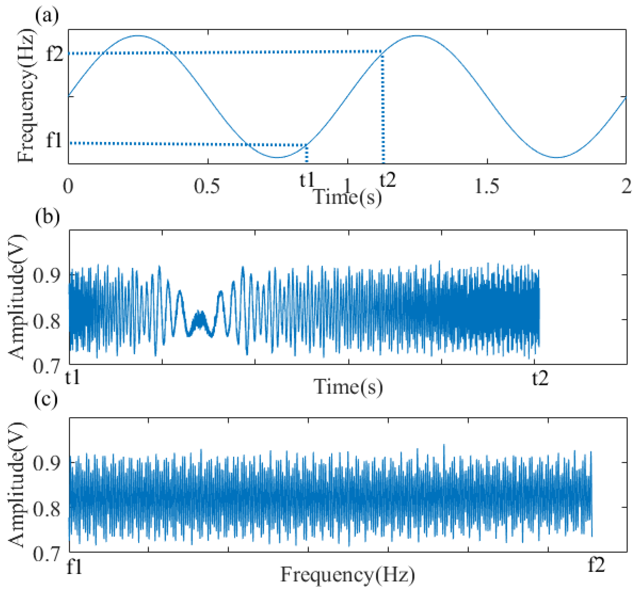
As shown in Figure 1a,b, a frequency-monotonic interval (f1, f2) is selected from the original frequency-modulated signal, along with the ranging interference signal corresponding to the time interval (t1, t2) is selected. After dividing the frequency interval (f1, f2) equally, the piecewise cubic hermite interpolating polynomial (PCHIP) interpolation method is used to insert discrete points on the coordinate axis of this evenly spaced frequency interval. These discrete points represent data extracted from Figure 1a,b, where the frequency is plotted on the x-axis and the corresponding interference signal intensity on the y-axis. After fitting with equally spaced frequencies, as depicted in Figure 1c, the interference signal becomes independent of time, and its frequency variation is uniform. Using this method, we successfully obtain interference signals with equal optical frequency intervals, from which distance information can be derived by performing a fast Fourier Transform (FFT).

Figure 1.
(a) Sine frequency modulation signal; (b) distance measuring interference signal; (c) distance measuring interference signal after equidistant fitting.
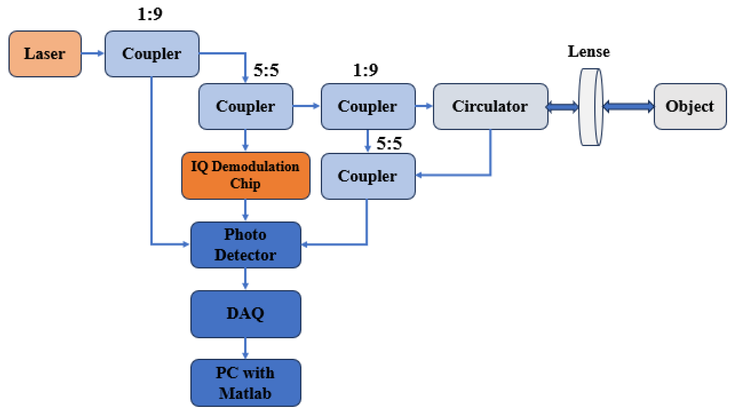
The experimental test system, depicted in Figure 2, features an all-fiber structure. The light source employs a standard commercial distributed feedback (DFB) laser with a central wavelength of 1310 nm and a linewidth of 200 kHz. The laser is driven by the CTL200 butterfly laser driver from Koheron, and a function generator produces a sinusoidal signal with a modulation period of 1kHz and modulation amplitude of 0.65 Vpp. After passing through a coupler, a portion of the light source signal enters an IQ demodulation chip. This chip includes a 7 m delay line Mach–Zehnder (MZ) interferometer, which extracts the frequency information of the sinusoidal frequency-modulated signal through IQ demodulation for further data processing.
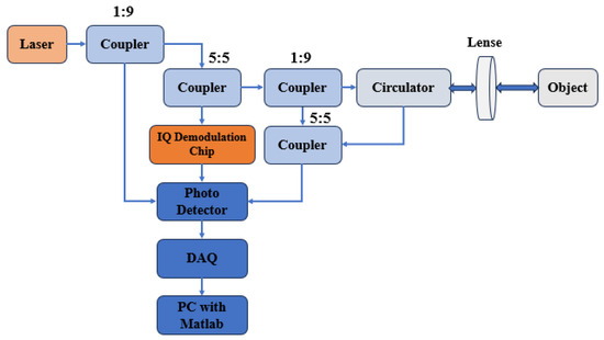
Figure 2.
Experimental system block diagram.
The remaining portion of the signal passes through a 1:9 coupler and functions as both the local oscillator and the main beam of the test system. The ranging main beam, after passing through a polarization-maintaining circulator, is emitted into the object space by a lens. The target object, a diffuse reflection board with 75% reflectivity, has a surface that is characterized as a uniform Lambertian surface. The main beam, reflected by the object, returns along its path to the circulator and merges with the local oscillator light at the balanced photodetector. The differential amplification circuit within the balanced photodetector effectively suppresses the common-mode signal and amplifies the differential-mode signal. Consequently, balanced detection effectively suppresses the DC component of the beat frequency signal and enhances the interference signal. The photodetector (PD) module, as shown in the figure, consists of three single-ended photodetectors and one balanced photodetector. All optical signals received by the PD are converted into digital signals by a digital acquisition card and subsequently processed and analyzed by a computer.
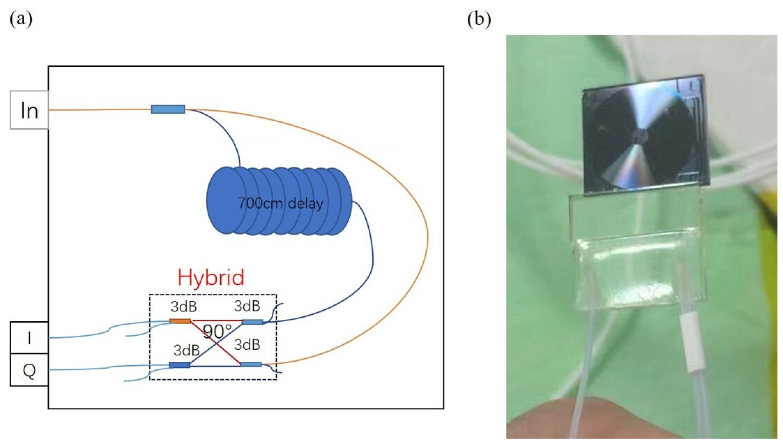
As shown in Figure 3, the IQ demodulation chip utilizes an asymmetric MZ interferometer structure. The input light is divided into two paths by a coupler, with one path passing through a 7-m-long waveguide structure to introduce a delay. The total loss for this 7-m waveguide is 14 dB. The 7-m-long waveguide is arranged in a spiral configuration, occupying an area of approximately 1 square centimeter. After the delay, the two paths are combined using a 2 × 4 mixer structure. The four output ports exhibit mixing phases of 0°, 90°, 180°, and 270°, respectively, with the 0° and 90° ports selected as the IQ signal outputs. The chip is packaged with an optical fiber array to facilitate signal input and output.

Figure 3.
(a) IQ demodulation chip block diagram; (b) physical image of the IQ demodulation chip.
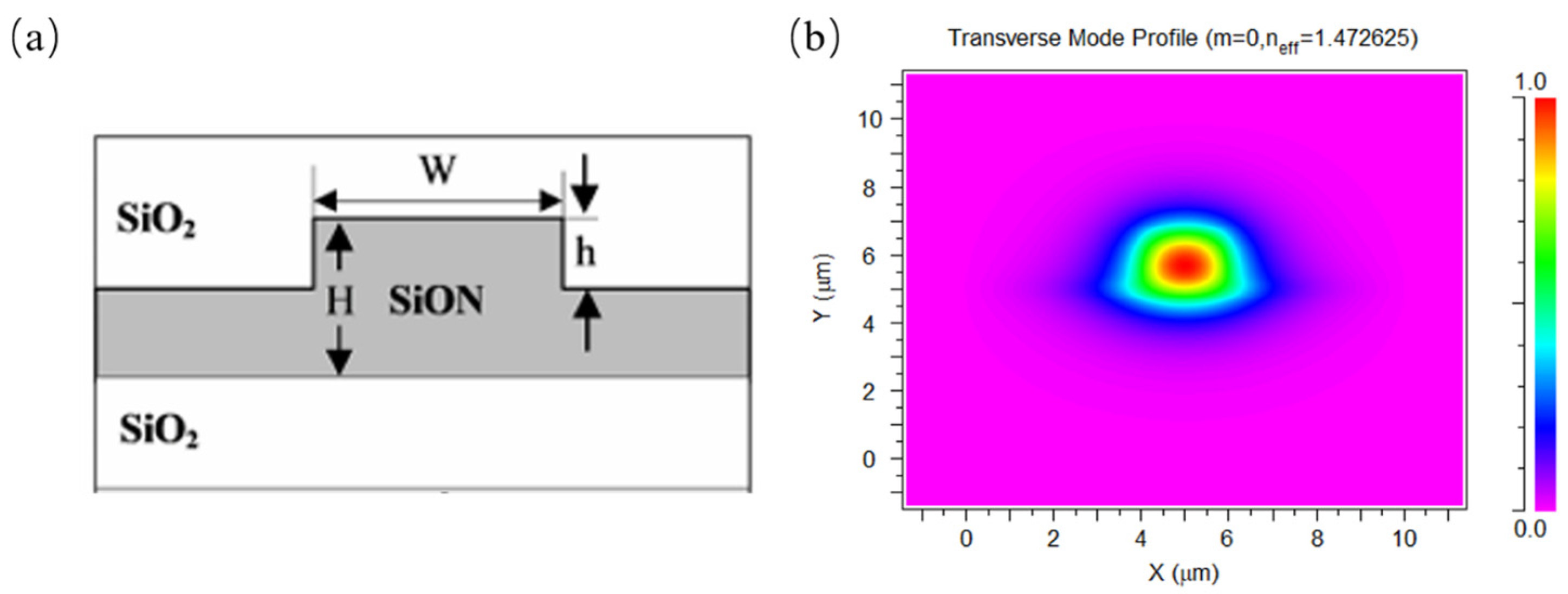
The chip utilizes SiON as the core material, which exhibits lower transmission loss (<0.4 dB/m) compared to other dielectrics, thereby making it more suitable for sensor applications than alternative optical integration platforms. Sensors designed for coherent detection typically incorporate long waveguide delay lines. The low loss of SiON allows the design to forgo optical amplification units, thereby simplifying the design and enhancing reliability. We employed RSoft CAD v2018.12 software to compute the effective refractive index and field distribution of the SiON waveguide modes. As shown in Figure 4, the effective refractive index at a wavelength of 1310 nm, given the illustrated structural parameters and TE polarization, is approximately 1.47.

Figure 4.
(a) Schematic cross-section of the SiON waveguide structure. W = 1 μm, H = 2 μm, h = 1.5 μm. (b) Simulation results of waveguide mode field distribution at 1310 nm wavelength.
Figure 5 illustrates the simulation results for the coupler structure in the on-chip interferometer, achieving a 5:5 splitting ratio through the use of cascaded couplers. The multi-stage couplers provide greater flexibility, enabling various splitting ratios by adjusting the coupling efficiency and length of each stage. This design effectively mitigates the impact of optical path cross-coupling and enhances system stability. Additionally, the cascaded directional couplers are linked through non-coupled sections that introduce phase shifts. This design eliminates errors introduced by the front-end coupler, facilitating the development of polarization- and fabrication-insensitive splitting devices [18].
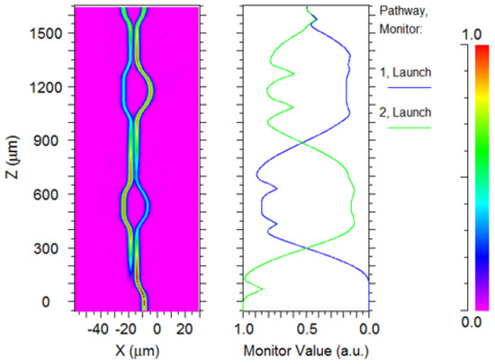
Figure 5.
Simulated results of a coupler.
In practical applications, optical waveguides are often configured in curved arrangements. When an optical waveguide bends, it disrupts the original spatial refractive index distribution, leading to partial leakage of optical energy and resulting in losses. SiON has a refractive index ranging from 1.5 to 2. Its tunable refractive index not only supports the design of multi-layer structures but also provides a greater refractive index contrast compared to silica cladding (with a refractive index of 1.45). This characteristic not only mitigates high waveguide losses and scattering observed in platforms such as SOI (silicon-on-insulator) but also permits smaller waveguide bending radii, thereby ensuring appropriate integration density. Table 1 lists the loss and bending radii of different materials. We simulated light field propagation in an S-shaped waveguide with varying refractive index differences, as illustrated in Figure 6. When the refractive index difference is 0.01, a significant portion of light leaks out, whereas, with a refractive index difference of 0.05, the light field is effectively confined within the waveguide.

Table 1.
Loss and bending radius of different materials.
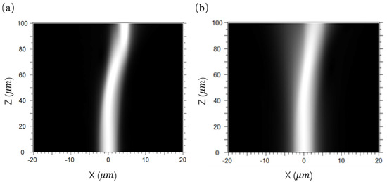
Figure 6.
Light field propagation with refractive index differences of 0.05 (a) and 0.01 (b).
The chip fabrication process is illustrated in the Figure 7. Initially, a silicon wafer is placed in an oxidation furnace for wet oxidation, resulting in the formation of dense SiO2 films on both sides of the wafer. Subsequently, a pure silica layer is deposited on the front side of the silicon wafer using plasma-enhanced chemical vapor deposition (PECVD) to serve as the lower cladding layer for the waveguide. A specially doped silica layer, SiON, is then deposited on the front side using PECVD to act as the core layer for the waveguide. The doping process is designed to ensure that the refractive index of the core layer exceeds that of the cladding layer. Photoresist is then spin-coated and patterned using photolithography and development processes to transfer the designed pattern from the mask to the photoresist. The photoresist is subsequently employed as a mask material for etching with a plasma etching machine, thereby transferring the pattern from the photoresist to the core layer. After the etching process, the remaining photoresist is removed, and a pure silica layer is deposited to form the upper cladding layer. Finally, the chip undergoes annealing to eliminate voids that formed during the deposition of the upper cladding layer. The final steps involve cutting, grinding, and polishing to produce individual chips.

Figure 7.
SiON waveguide fabrication process.
3. Experiment
3.1. Ranging Experiment
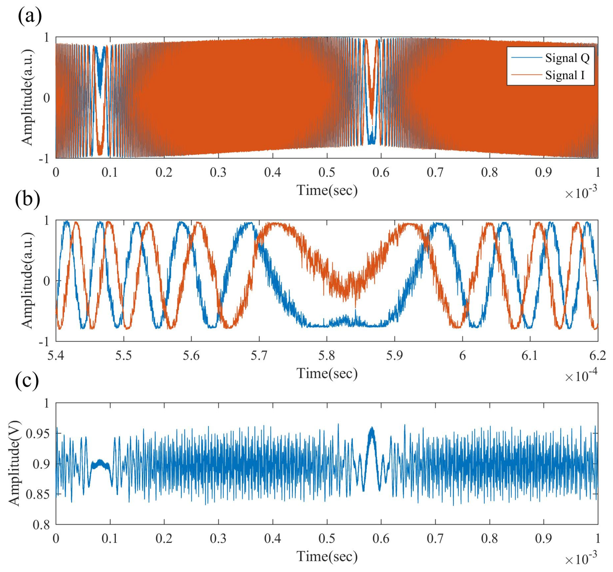
In the experiment, the frequency information of the sinusoidal frequency-modulated laser signal is initially acquired using an on-chip interferometer and a demodulation algorithm. The sinusoidal frequency-modulated signal emitted by the laser is directed into the on-chip interferometer, where its orthogonal phase components are extracted through IQ signal decomposition. Figure 8a,b depicts the normalized IQ signals and their respective partial magnifications. Notably, deviations in manufacturing processes, errors in waveguide design, and interference from system noise can all lead to phase deviations in the IQ signals. Consequently, the actual IQ signals are not perfectly orthogonal. This phase error was mitigated by adjusting the mixing angle, followed by demodulation to extract the frequency information of the sinusoidal frequency-modulated signal. As shown in Figure 9, the demodulated signal closely resembles a perfect sinusoidal curve with a period of 1 kHz, consistent with the modulation period of the signal generator output. This result validates the accuracy of our method for IQ demodulation of the laser modulation signal. Furthermore, the on-chip interferometer utilizing SiON waveguides demonstrates lower noise and reduced signal loss compared to fiber optic pathways. This characteristic ensures the reliability of the IQ-demodulated signals.
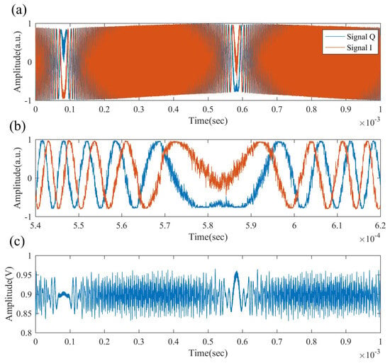
Figure 8.
Signals received by the photodetector. (a) Normalized IQ signals from the on-chip interferometer. (b) Partially magnified view of the normalized IQ signals from the on-chip interferometer. (c) Ranging interference signal containing the required distance information.
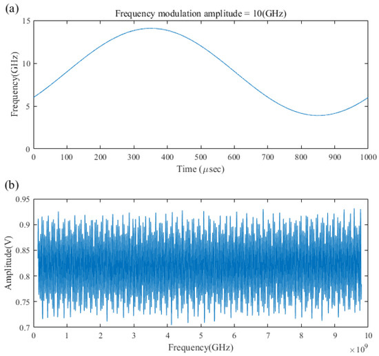
Figure 9.
Frequency-modulated signal and fitting. (a) Actual sinusoidal frequency-modulated signal from the laser. (b) Measured interference signal after equal frequency interval fitting.
Furthermore, the calculated bandwidth of the modulation signal is 10 GHz. In FMCW laser ranging, the distance resolution is given by the following formula:
where represents the distance resolution, the speed of light, and the modulation bandwidth. The system’s distance resolution is dependent on its modulation bandwidth. Calculations reveal that the theoretical distance resolution of this experimental system is 1.5 cm.
Subsequently, a monotonic interval is extracted from the sinusoidal frequency-modulated signal, while simultaneously, the corresponding measured interference signal is captured. The frequency change of the modulation signal is used as the horizontal coordinate, with the amplitude of the measured interference signal as the vertical coordinate. The PCHIP interpolation method is utilized for equal frequency interval fitting. The fitted signal is shown in Figure 9b, followed by the application of an FFT to derive the corresponding distance information. Prior to performing the FFT, the data must be preprocessed by converting it to a power of 2 for optimal handling, and a rectangular window is applied to minimize spectral leakage. After preprocessing, the number of data points is = 131,072, and the signal sampling frequency = 250 MHz. The resolution bandwidth (RBW) of the spectrum is calculated using the following formula, resulting in an approximate value of 1.9 kHz.
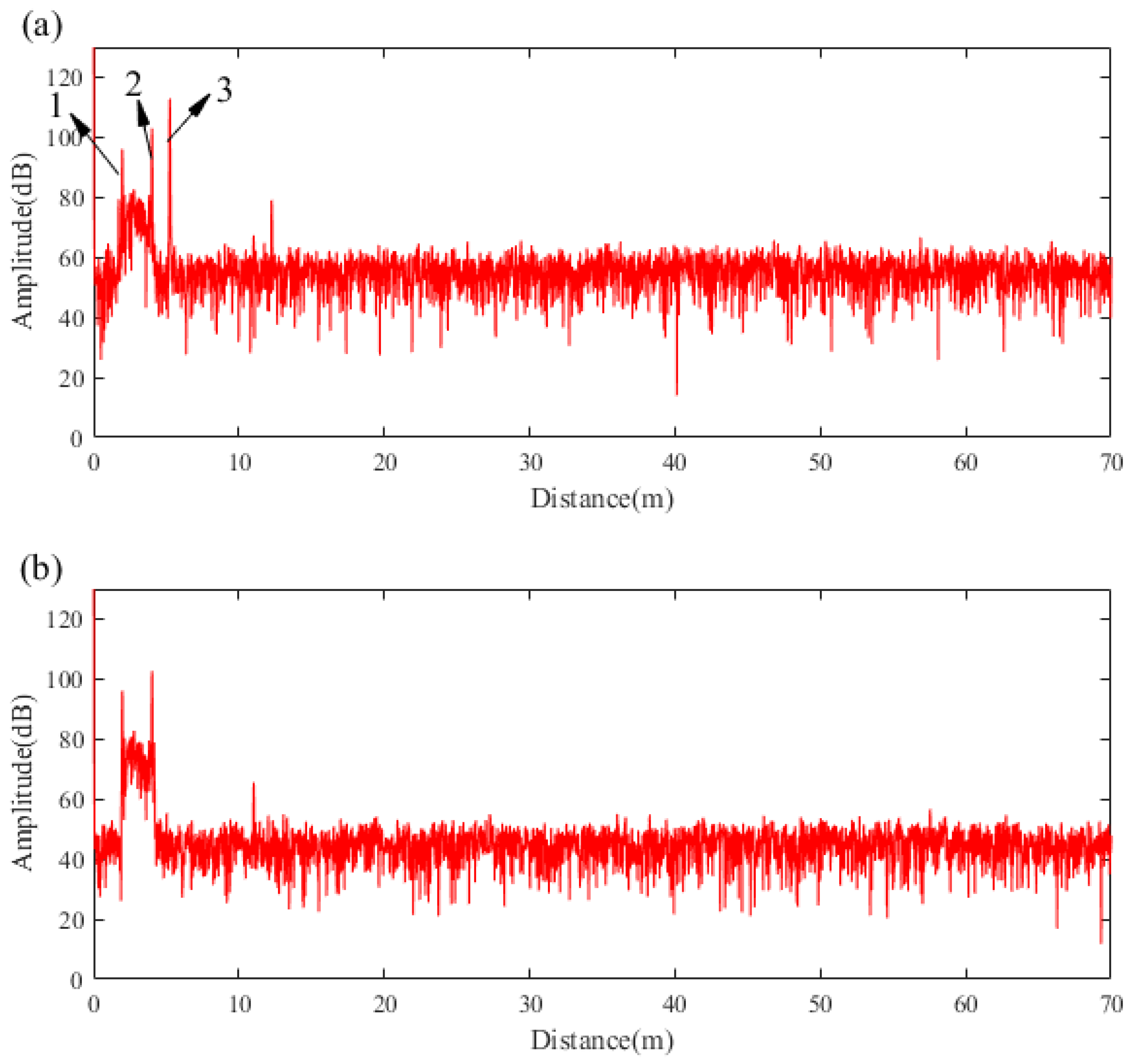
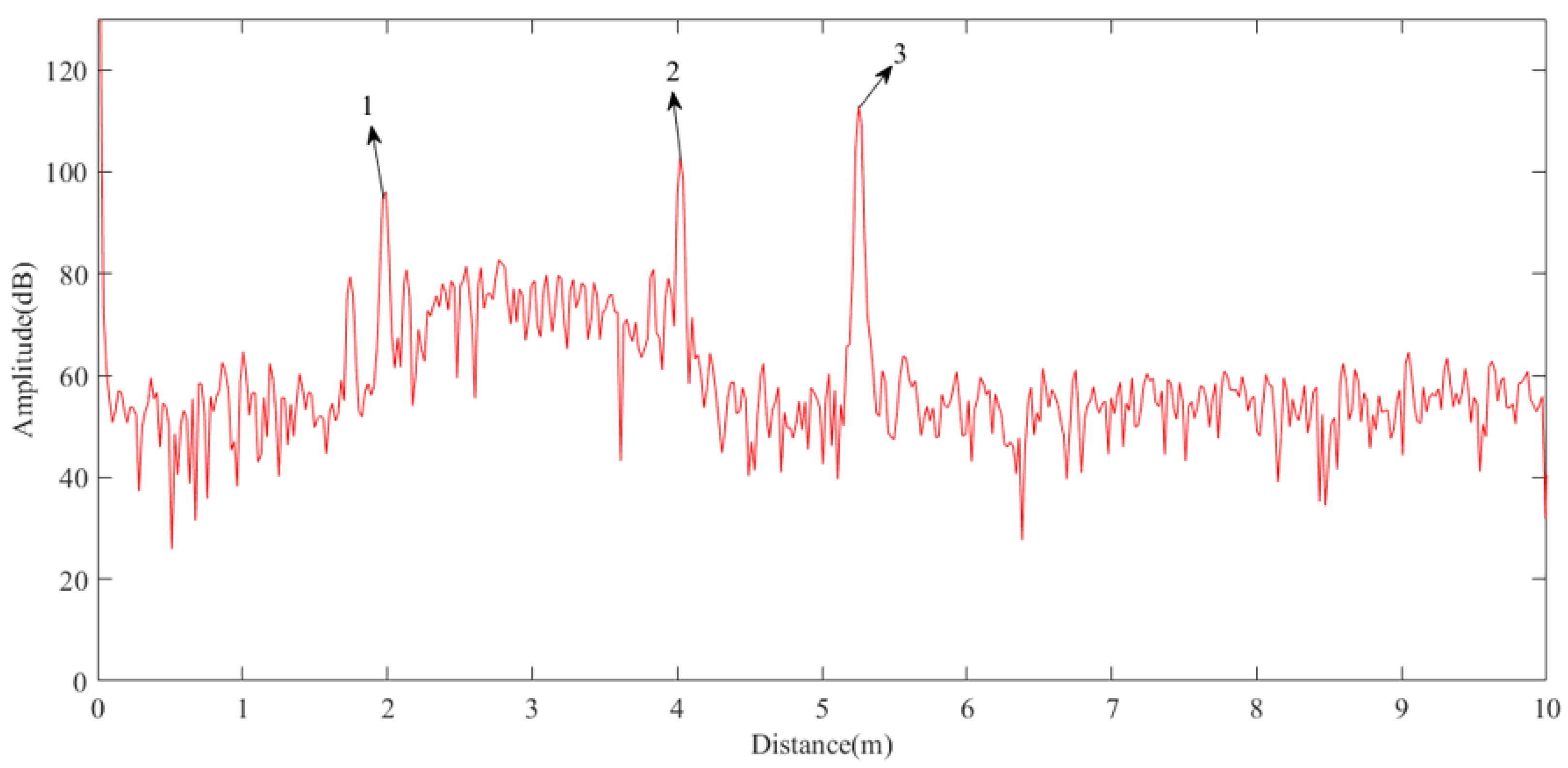
Figure 10 illustrates that, after performing the FFT, three predominant characteristic peaks are observed. After covering the lens and conducting the analysis, the results are as follows: peak 3 corresponds to the reflection from the measured object, serving as the characteristic peak necessary for ranging. Peaks 1 and 2, on the other hand, represent interferences from internal reflection points within the polarization-maintaining circulator. Peaks 1 and 2, being inherent system interferences, appear in the forward region of the spectrum and do not contribute to crosstalk in the ranging results. A spurious signal of noticeable intensity was detected at 12 m. Subsequent experiments suggest that this signal results from environmental noise, as similar spurious peaks did not consistently appear at this distance but rather at random positions with varying intensities. This does not significantly impact our experimental measurements. Firstly, the intensity of such random noise is relatively low. Moreover, our ranging algorithm preliminarily determines the range of characteristic peaks through theoretical calculations, thus mitigating the influence of spurious peaks at other positions. Furthermore, peak 2 serves as a reference point for monitoring changes in system power, as its intensity is solely influenced by the output power of the laser, reflecting the stability of the test system to some extent. Figure 11 provides a local magnification of the three characteristic peaks shown in Figure 10a. It is evident that there is no significant broadening of each peak in the target distance spectrum; each peak remains sharp and distinct, allowing for easy differentiation of the spectral peak corresponding to the measured distance. This clarity establishes a solid foundation for long-distance detection.

Figure 10.
FFT results of the ranging signal. (a) With the lens uncovered. (b) With the lens covered.
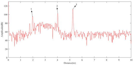
Figure 11.
Details of the characteristic peak.
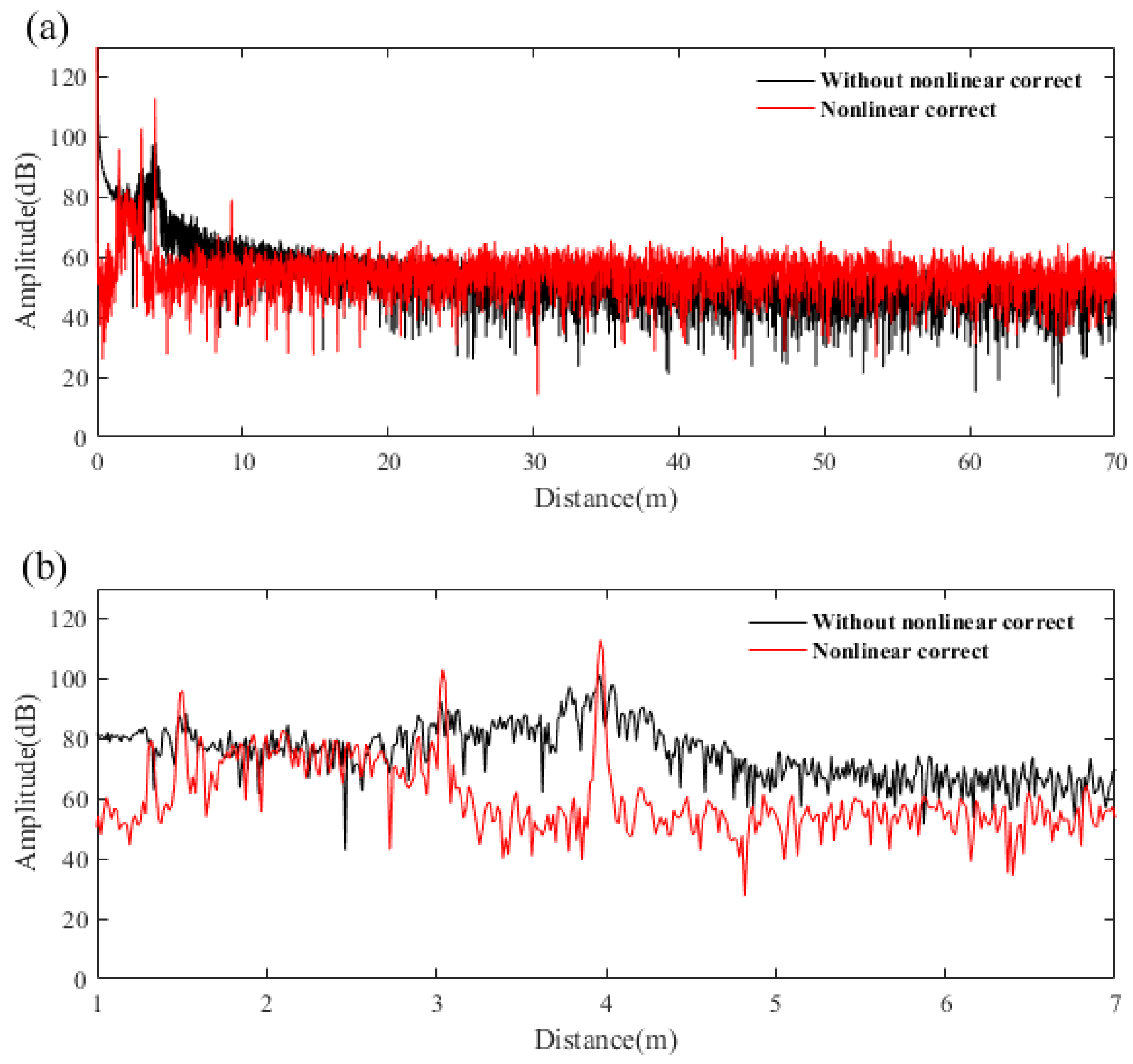
To validate the reliability of the sinusoidal signal nonlinear correction method proposed in this study, a comparative analysis was performed using the unprocessed ranging interference signal. Figure 12 illustrates the power spectrum obtained via FFT of the unprocessed ranging interference signal. It is evident that direct FFT of the ranging interference signal leads to a substantial broadening of the spectrum at the original characteristic peak, accompanied by a significant reduction in signal contrast and measurement resolution. However, by adopting the equal frequency interval fitting method proposed in this study, the central frequency value of the characteristic peak corresponding to the measured target can be accurately determined, and the distance can be calculated. This approach effectively mitigates spectral broadening of the measurement light signal, thereby enhancing the stability of distance extraction corresponding to the measured target.

Figure 12.
Spectrum of the measured signal. (a) Comparison before and after nonlinear correction. (b) Detailed view of (a).
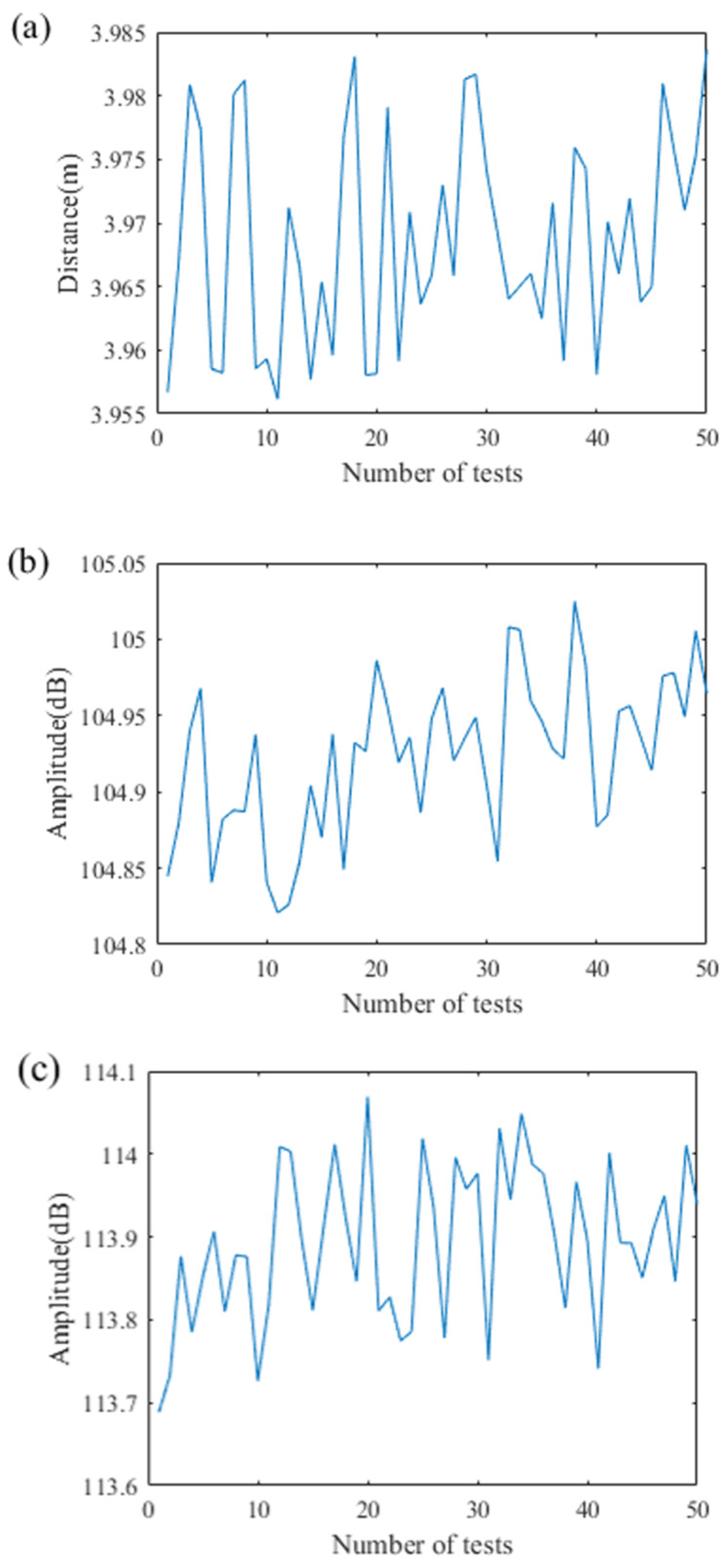
It is important to note that the ranging results obtained in our experiments have been converted to free-space distance. At a distance of 3.97 m, 50 repeated measurements were conducted. The MATLAB timer function recorded that 50 measurements took approximately 60 s. As illustrated in Figure 13a, the results from the 50 ranging experiments showed a fluctuation range of 0.0262 m, with a maximum absolute measurement error of 0.012 m. Figure 13b depicts the power fluctuation of peak 2 from Figure 10a, reflecting the internal stability of the laser output and the testing system. Similarly, we analyzed the power fluctuation of characteristic peak 3 from Figure 10a to assess the stability of the target detection data during system operation. The results indicate that, across 50 repeated measurements, the power fluctuation ranges were 0.204 dB and 0.38 dB, respectively. This level of accuracy and stability holds promise for practical applications.
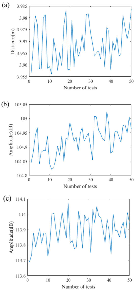
Figure 13.
Ranging experiment results at 3.97 m. (a) Distance repeatability experiment. (b) Power fluctuation of peak 2. (c) Power fluctuation of peak 3.
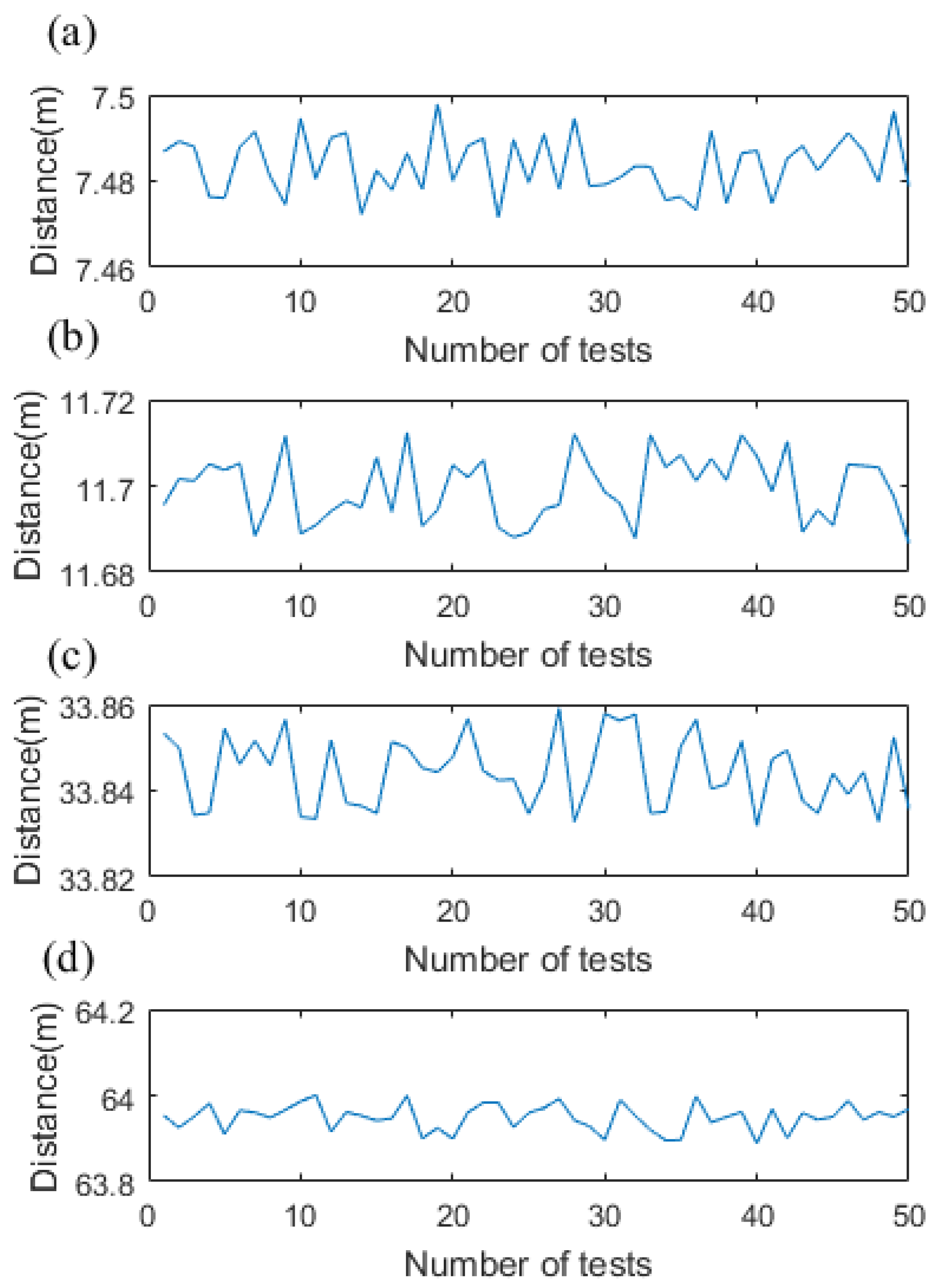
Additional experiments were performed at various distances, with the specific results illustrated in Figure 14. Measurements were repeated 50 times at distances of 7.48, 11.69, 33.84, and 63.95 m, with the fluctuation ranges and maximum absolute errors summarized in Table 2. It was observed that at distances less than 33.84 m, there was no significant change in the fluctuation range or maximum error as the distance increased. However, at a distance of 63.95 m, a noticeable change was observed in both the fluctuation range and maximum error. This can be attributed to a significant reduction in the intensity of the interference signal and the system’s signal-to-noise ratio at this extended distance, compounded by pronounced environmental influences, leading to increased variability in the experimental results. These findings suggest that the FMCW laser ranging system developed in this study exhibits consistent repeatability and stability as the test distance increases, with a maximum tested range of 63.95 m.
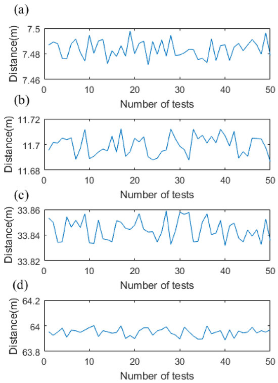
Figure 14.
Results of long-distance ranging experiments. (a) 7.48 m. (b) 11.69 m. (c) 33.84 m. (d) 63.95 m.

Table 2.
Experimental results at different distances.
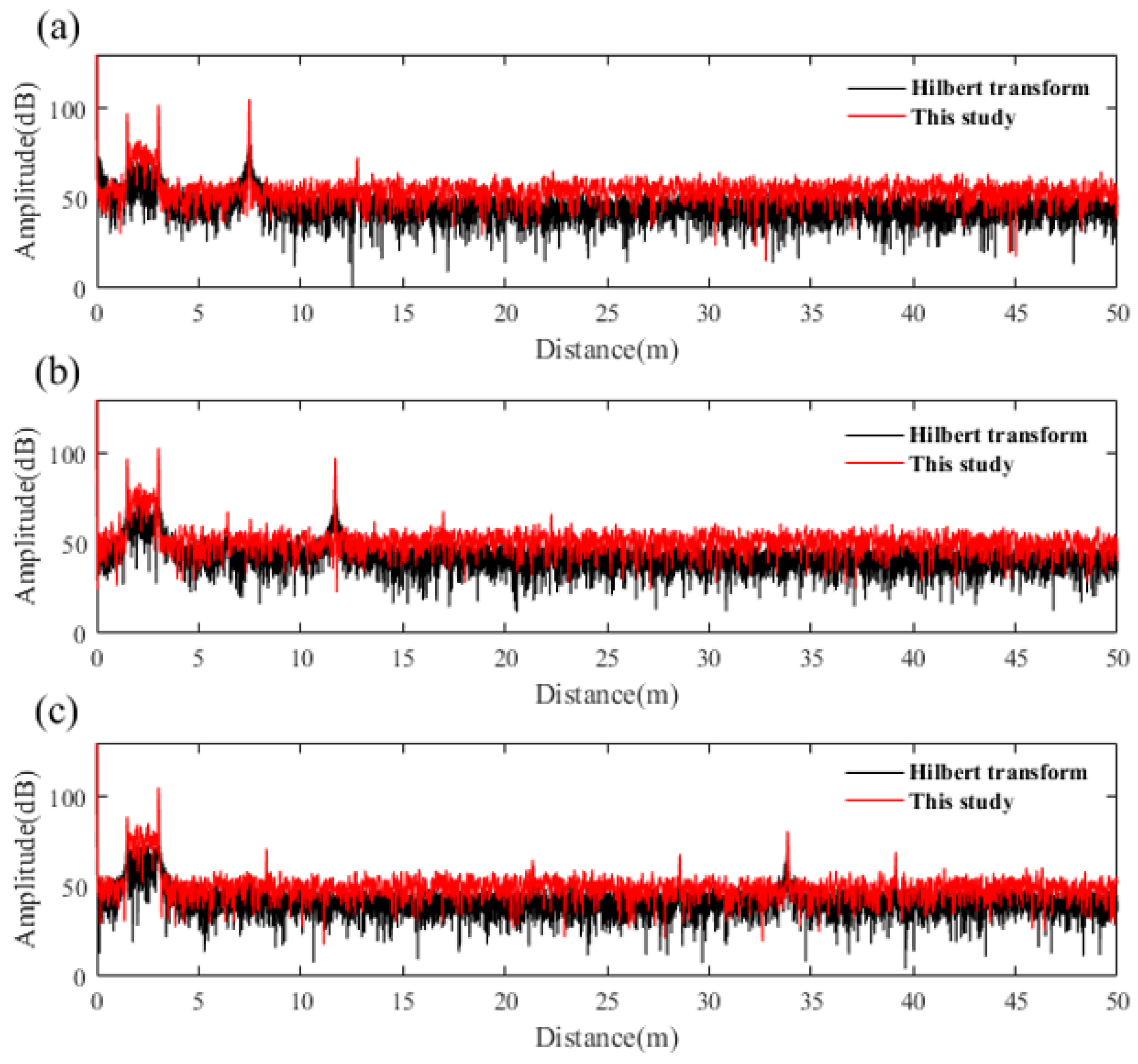
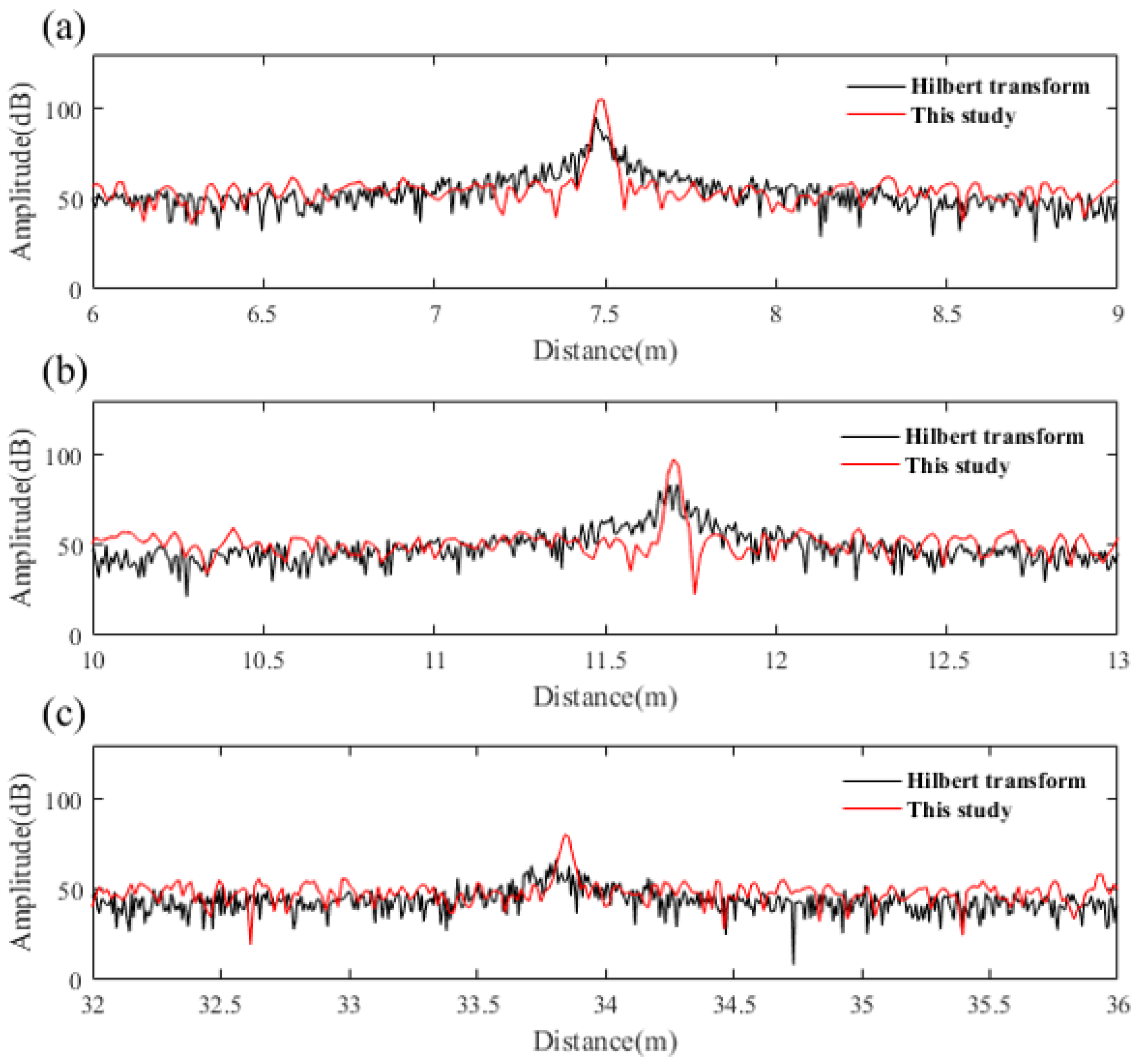
Additionally, experimental data at distances of 7.48, 11.69, and 33.84 m were selected for spectral analysis and processed using the Hilbert transform method. These results were compared with those obtained in this study, as illustrated in Figure 15 and Figure 16. Figure 15a–c displays the results from this study alongside those processed using the Hilbert transform. Both datasets exhibit characteristic peaks at corresponding distance positions. For enhanced analysis, the characteristic peaks were magnified. Figure 16, which presents magnified views, shows that the results from this study exhibit distinct, sharp peaks at all distances, which remain clearly defined even after magnification, without interference from sidelobes. In contrast, after applying the Hilbert transform, the characteristic peaks show considerable spectral broadening at shorter distances. Furthermore, as the detection distance increases, the spectral broadening becomes progressively more severe, with multiple sidelobes emerging. This results in a significant reduction in detection signal contrast, which is detrimental to long-range detection. This indicates that the Hilbert transform does not fully correct the nonlinearity of the sinusoidal frequency-modulated signal.
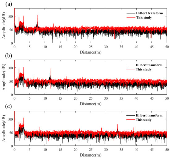
Figure 15.
This study is compared with the Hilbert transform processing. (a) 7.48 m (b) 11.69 m (c) 33.84 m.
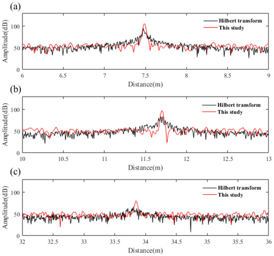
Figure 16.
Detailed view of Figure 15. (a) 7.48 m (b) 11.69 m (c) 33.84 m.
To quantitatively analyze the differences between the two methods, we conducted 50 repeated experiments using the Hilbert transform method at three different distances. We computed the maximum ranging error and the range of fluctuation in ranging. Due to the spectrum widening phenomenon and sidelobe interference in the spectrum resulting from the Hilbert transform, accurate distance values could not be determined. Consequently, we selected the midpoint of the peak with a 3 dB drop as the ranging range and averaged these values to obtain the distance estimation. The specific data are presented in Table 3, and a comparison with Table 1 clearly demonstrates that the repeatability of the experimental results obtained using the Hilbert transform method deteriorated, with a significant increase in maximum error and fluctuation range compared to our method. Moreover, as the distance increased, the spectrum-widening phenomenon intensified, resulting in a more pronounced increase in error. The experimental results demonstrate that the method proposed in our study exhibits higher ranging accuracy and reduced ranging errors compared to the traditional Hilbert transform method.

Table 3.
Experimental results of the Hilbert transform at different distances.
3.2. Ranging Accuracy and Distance Resolution
The random measurement error at various distances was analyzed using Equation (9) to assess the ranging accuracy of the FMCW laser ranging system. The formula is expressed as follows:
Here, represents the ranging error, denotes the measurement distance value of the -th measurement, indicates the average ranging value, and represents the total number of valid measurements. Detailed data are provided in Table 4. Consistent with the patterns observed in the previously discussed ranging experiment results, no significant change in ranging accuracy is observed for distances up to 33.84 m. However, at a distance of 63.95 m, the accuracy significantly decreases, attributable to the same factors previously analyzed.

Table 4.
Ranging accuracy.
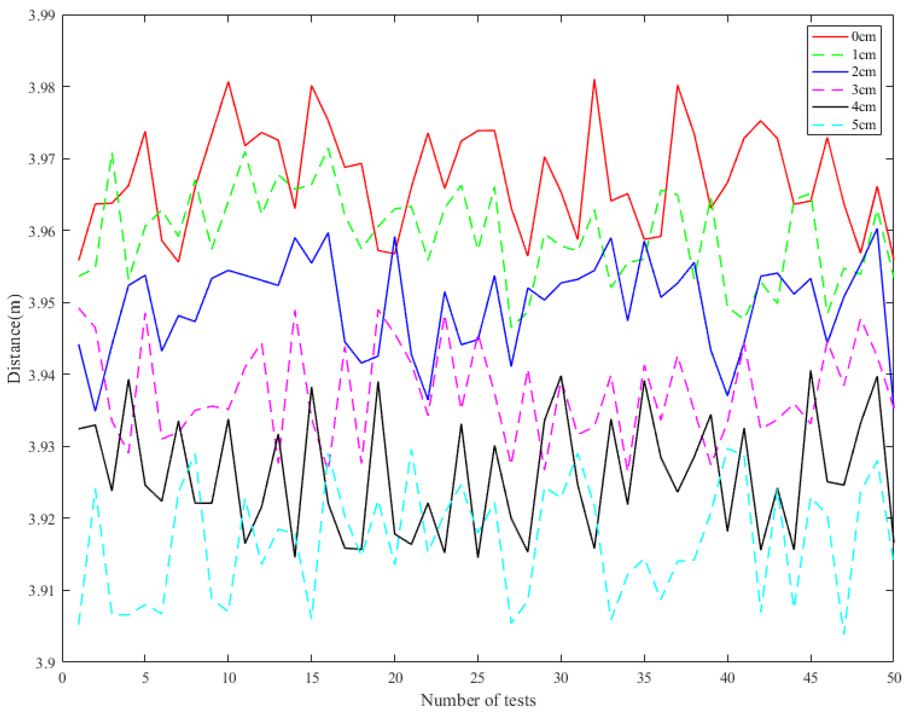
Furthermore, experiments were conducted to determine the system’s distance resolution. The emitted signals of the FMCW laser radar were incident perpendicularly on a reflection board, which, fixed to a motor, moved back and forth along the optical path, advancing by 0.01 m each time. As depicted in Figure 17, each experimental result fluctuates within a specific distance range. Therefore, the system’s distance resolution is defined as follows: if the fluctuation range of the results does not significantly affect the outcomes at two different distances, it is inferred that the system can distinguish the distance difference between these measurements. Observing the results in Figure 17, it is evident that when the motor advances by 0.02 m, as exemplified at 0, 2, and 4 cm or 1, 3, and 5 cm, the fluctuation ranges of the results either do not interfere with each other or have minimal effect. Consequently, the distance resolution of the experimental system in this study is approximately 2 cm. Considering experimental errors and noise, this value aligns with the theoretically calculated resolution of 1.5 cm.
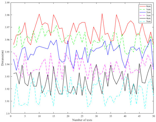
Figure 17.
Results of the distance resolution experiment.
3.3. Calculation of System Signal-to-Noise Ratio (SNR)
The signal-to-noise ratio of the experimental system directly affects the ranging scope, accuracy, and distance resolution. A higher SNR enables detection over greater distances. The of the FMCW laser ranging system in this study is described by the following equation:
Here, represents the total noise power, which includes three components: laser intensity noise , photodetector (PD) shot noise , and electronic noise These components are calculated as follows:
In these equations, represents the relative intensity noise of the laser, measured at −145 dB/Hz in preliminary tests; P denotes the laser power, specifically the intrinsic light power measured on the PD at the balanced detector, is the responsivity of the PD at 0.9 A/W, is the transimpedance amplifier gain of the balanced detector at 39,000 V/A, is the imbalance of the two PDs in the balanced detector at 0.1, and is the bandwidth of the balanced detector at 100 MHz. Additionally, the term in the equation represents the equivalent noise current density of the driving circuit.
The strength of the return light signal and the SNR measured by the system are determined by the following equation:
Here, denotes the return light power. The system’s emitted ranging laser power is 12.4 dBm, and with a return light loss of approximately 40 dB, this results in being −27.6 dBm. The calculated SNR of this test system is 55.3 dB. Theoretical calculations demonstrate that the experimental system proposed in this study possesses a high SNR, which is conducive to long-distance, high-accuracy, and high-resolution target detection.
4. Conclusions
This paper investigates the principle of nonlinear correction in FMCW, employing an on-chip interferometer and IQ demodulation technology to compute the frequency information of the frequency-modulated signal for interpolation fitting. Additionally, we utilized an on-chip interferometer designed with SiON waveguides, which resulted in reduced noise and loss. This advancement enhances the capabilities of precision measurement technology based on photonic integrated circuits. The experiments effectively corrected the nonlinearity of the sinusoidal signal, resulting in a maximum measurement error of 0.012 m, a ranging resolution of 2 cm, and a maximum signal-to-noise ratio of 55.3 dB over a distance range of 3.97 m to 63.95 m.
Author Contributions
Conceptualization, L.Z. (Leifu Zhou), Y.Q., T.C. and T.L.; data curation, L.Z. (Lijuan Zhang); funding acquisition, L.Z. (Lijuan Zhang); methodology, L.Z. (Leifu Zhou), L.Z. (Lijuan Zhang) and T.L.; project administration, T.C.; resources, L.Z. (Lijuan Zhang); software, L.W.; supervision, L.Z. (Lijuan Zhang) and T.C.; validation, L.Z. (Leifu Zhou); writing—original draft preparation, L.Z. (Leifu Zhou); writing—review and editing, X.M., L.Z. (Lijuan Zhang) and T.C. All authors have read and agreed to the published version of the manuscript.
Funding
The research is partially funded by Zhejiang Provincial Natural Science Foundation Youth Fund Project (Grant No. LQ23F010004), the National Natural Science Youth Science Foundation Project (Grant No. 62201508) and Zhejiang Provincial Natural Science Foundation of China under Grant No. LQ21F050003.
Institutional Review Board Statement
Not applicable.
Informed Consent Statement
Not applicable.
Data Availability Statement
Data are contained within the article.
Conflicts of Interest
Author Lei Wang was employed by the company OmniSensing Photonics Technology Co., Ltd. The remaining authors declare that the research was conducted in the absence of any commercial or financial relationships that could be construed as a potential conflict of interest.
References
- Feneyrou, P.; Leviandier, L.; Minet, J.; Pillet, G.; Martin, A.; Dolfi, D.; Schlotterbeck, J.-P.; Rondeau, P.; Lacondemine, X.; Rieu, A.; et al. Frequency-modulated multifunction lidar for anemometry, range finding, and velocimetry–1. Theory and signal processing. Appl. Opt. 2017, 56, 9663–9675. [Google Scholar] [CrossRef] [PubMed]
- Song, Z.Q.; Zhu, J.G.; Xie, T.P.; Feng, L.; Yan, J. Research progress on security LiDAR. Laser Optoelectron. Progress 2021, 58, 28–42. [Google Scholar]
- Royo, S.; Ballesta-Garcia, M. An overview of lidar imaging systems for autonomous vehicles. Appl. Sci. 2019, 9, 4093. [Google Scholar] [CrossRef]
- Behroozpour, B.; Sandborn, P.A.M.; Wu, M.C.; Boser, B.E. Lidar system architectures and circuits. IEEE Commun. Mag. 2017, 55, 135–142. [Google Scholar] [CrossRef]
- Zheng, J. Optical frequency-modulated continuous-wave interferometers. Appl. Opt. 2006, 45, 2723–2730. [Google Scholar] [CrossRef] [PubMed]
- Zheng, J. Reflectometric fiber optic frequency-modulated continuous-wave interferometric displacement sensor. Opt. Eng. 2005, 44, 124404. [Google Scholar] [CrossRef]
- Jia, L.H.; Wang, Y.; Wang, X.Y.; Zhang, F.; Wang, W.; Wang, J.; Zheng, J.; Chen, J.; Song, M.; Ma, X.; et al. Nonlinear calibration of frequency modulated continuous wave LIDAR based on a microresonator soliton comb. Opt. Lett. 2021, 46, 1025–1028. [Google Scholar] [CrossRef] [PubMed]
- Li, C.L.; Liu, J.C.; Zhang, F.M.; Qu, X. Review of nonlinearity correction of frequency modulated continuous wave LiDAR measurement technology. Opto-Electron. Eng. 2022, 49, 210438. [Google Scholar]
- Lu, C.; Liu, G.; Liu, B.; Chen, F.; Gan, Y. Absolute distance measurement system with micron-grade measurement uncertainty and 24 m range using frequency scanning interferometry with compensation of environmental vibration. Opt. Express 2016, 26, 30215–30224. [Google Scholar] [CrossRef] [PubMed]
- Di Lazaro, T.; Nehmetallah, G. Multi-terahertz frequency sweeps for high-resolution, frequency-modulated continuous wave ladar using a distributed feedback laser array. Opt. Express 2017, 3, 2327–2340. [Google Scholar] [CrossRef] [PubMed]
- Mateo, A.B.; Barber, Z.W. Precision and accuracy testing of FMCW ladar-based length metrology. Appl. Opt. 2015, 19, 6019–6024. [Google Scholar] [CrossRef] [PubMed]
- Iiyama, K.; Wang, L.T.; Hayashi, K.I. Linearizing optical frequencysweep of a laser diode for FMCW reflectometry. J. Light. Technol. 1996, 14, 173–178. [Google Scholar] [CrossRef]
- Glombitza, U.; Brinkmeyer, E. Coherent frequency-domain reflectometry for characterization of single-mode integratedoptical waveguides. J. Lightwave Technol. 1993, 11, 1377–1384. [Google Scholar] [CrossRef]
- Ahn, T.J.; Lee, J.Y.; Kim, D.Y. Suppression of nonlinear frequency sweep in an optical frequency-domain reflectometer by use of Hilbert transformation. Appl. Opt. 2005, 44, 7630–7634. [Google Scholar] [CrossRef] [PubMed]
- Rosenfeldt, H.; Knothe, C.; Cierullies, J.; Brinkmeyer, E. Evolution of amplitude and dispersion spectra during fiber Bragg grating fabrication. In Bragg Gratings, Photosensitivity, and Poling in Glass Waveguides; Optica Publishing Group: Stresa, Italy, 2001; Volume 7, Number 4; p. BWA4. [Google Scholar]
- Badar, M.; Lu, P.; Buric, M.; Ohodnicki, P.O. Integrated auxiliary interferometer for self-correction of nonlinear tuning in optical frequency domain reflectometry. J. Light. Technol. 2020, 38, 6097–6103. [Google Scholar] [CrossRef]
- Zhang, X.B.Q.; Kong, M.; Guo, T.T.; Zhao, J.; Wang, D.; Liu, L.; Liu, W.; Xu, X. Frequency modulation nonlinear correction and range-extension method based on laser frequency scanning interference. Appl. Opt. 2021, 60, 3446–3451. [Google Scholar] [CrossRef] [PubMed]
- Little, B.E.; Murphy, T. Design rules for maximally flat wavelength-insensitive optical power dividers using Mach-Zehnder structures. IEEE Photonics Technol. Lett. 1997, 9, 1607–1609. [Google Scholar] [CrossRef]
Disclaimer/Publisher’s Note: The statements, opinions and data contained in all publications are solely those of the individual author(s) and contributor(s) and not of MDPI and/or the editor(s). MDPI and/or the editor(s) disclaim responsibility for any injury to people or property resulting from any ideas, methods, instructions or products referred to in the content. |
© 2024 by the authors. Licensee MDPI, Basel, Switzerland. This article is an open access article distributed under the terms and conditions of the Creative Commons Attribution (CC BY) license (https://creativecommons.org/licenses/by/4.0/).

