Article

Design of a High-Frame-Rate and Large-Grayscale Simulation Projection System Based on Digital Micromirror Devices

1
Changchun Institute of Optics, Fine Mechanics and Physics, Chinese Academy of Sciences, Changchun 130033, China
2
University of Chinese Academy of Sciences, Beijing 100049, China
*
Author to whom correspondence should be addressed.
Photonics 2024, 11(9), 793; https://doi.org/10.3390/photonics11090793
Submission received: 4 July 2024 / Revised: 22 August 2024 / Accepted: 22 August 2024 / Published: 26 August 2024
(This article belongs to the Special Issue Fundamentals, Advances, and Applications in Optical Sensing)

Abstract

:
With the increasing acquisition speed of image sensors, it has become necessary to provide image sources with higher frame rates and grayscale in order to meet testing requirements. In the field of semi-physical simulation projection, digital micromirror devices are often chosen for their high resolution, uniformity, response speed, and energy concentration. In this study, we utilized digital micromirror devices to construct a high-frame-rate and large-grayscale simulation projection system. To achieve our experiment goals, we employed two digital micromirror devices. One DMD was used to modulate the light intensity of the light source, while the other generated images with different bit planes. By projecting the target images onto the image sensor, we were able to achieve a frame rate of 1611 hz for the projected 12-bit image. This system meets the requirements for our experiment design and ensures the accurate testing of image sensors.

1. Introduction

A digital micromirror device (DMD) is an optical micro-electrical-mechanical system (MEMS) that contains an array of highly reflective aluminum micromirrors [1]. It is a display device that is monolithically integrated into the CMOS static random access memory (SRAM) [2]. The DMD operates by moving the micromirrors rapidly through electrostatic force [3,4], allowing the reflected light to be projected onto a screen through a lens, resulting in bright pixels. Each micromirror has two operating states, deflected by ±12° with respect to the micromirror axis [5]. The micromirrors can be deflected by a fixed angle based on the data from its corresponding CMOS storage unit and held for a specified period of time. This process enables the creation of images with a specific grayscale and contrast on the target surface of the detector. The human visual system or an image detector can efficiently integrate these light pulses to perceive the desired intensity.
Digital micromirror devices (DMDs) offer numerous advantages, including high resolution, uniformity, frame rate, dynamic range, and complete digitization [6,7,8]. Additionally, DMDs have a high fill factor and pixel density, leading to improved light utilization, image resolution, and quality [9,10]. As a result, semi-physical simulation projection technology based on DMDs is widely utilized in various applications, such as spatial light and structured light modulation, 3D printing, advanced imaging, infrared hyperspectral imaging, and maskless lithography [11,12,13,14,15,16]. This technology has significantly advanced imaging technology, image sensor testing, and other related fields. With the continuous advancements in semiconductor technology and high-speed, high-quantization bit image sensors, the sampling speed of image sensors is increasing, leading to enhanced signal quality [17,18]. Traditional projection simulation systems are no longer sufficient to meet these evolving requirements. It is relatively easy to reach the frame rate limit for the grayscale modulation of a single DMD [19,20,21]. Utilizing image generation techniques with low frame rates and quantization bits can result in distortion and other negative effects during image acquisition, failing to meet the demands of high-speed image capture. Therefore, the challenge lies in achieving high-frame rates and quantization bit counts simultaneously in projection systems, presenting an urgent engineering problem that needs to be addressed.
In this paper, we present a novel solution, utilizing dual digital micromirror devices (DMDs) to address the limited frame rate and grayscale levels of DMD projection displays. For the projection optical path, we propose a method that involves simultaneously modulating the intensity of the light source and the grayscale levels of the projected image. This approach involves the use of two DMDs concurrently to modulate both the time and energy domains of the projection process. Through experimental verification and testing, we confirm that our system is capable of projecting analog scenes with 12 quantization bits at a frame rate of 1611 Hz for a single image. This innovative approach showcases the potential of dual DMDs in achieving high-frame rates and large grayscale levels in projection systems, demonstrating promising results for applications requiring high-speed image acquisition and the accurate testing of image sensors.

2. Principle

In traditional DMD pulse–width grayscale modulation, the light energy of various grayscale levels is adjusted by controlling the display duration of different bit planes. In contrast to this conventional grayscale modulation method, the projection process based on dual DMDs can be seen as realizing energy quantization and distribution within a specified spatial region of the target plane image sensor within a defined timeframe. This means that in addition to the original time domain modulation, energy domain modulation is also applied. This dual modulation approach enhances the quantization bit count of the projected image and simultaneously improves the frame rate of the projected image.

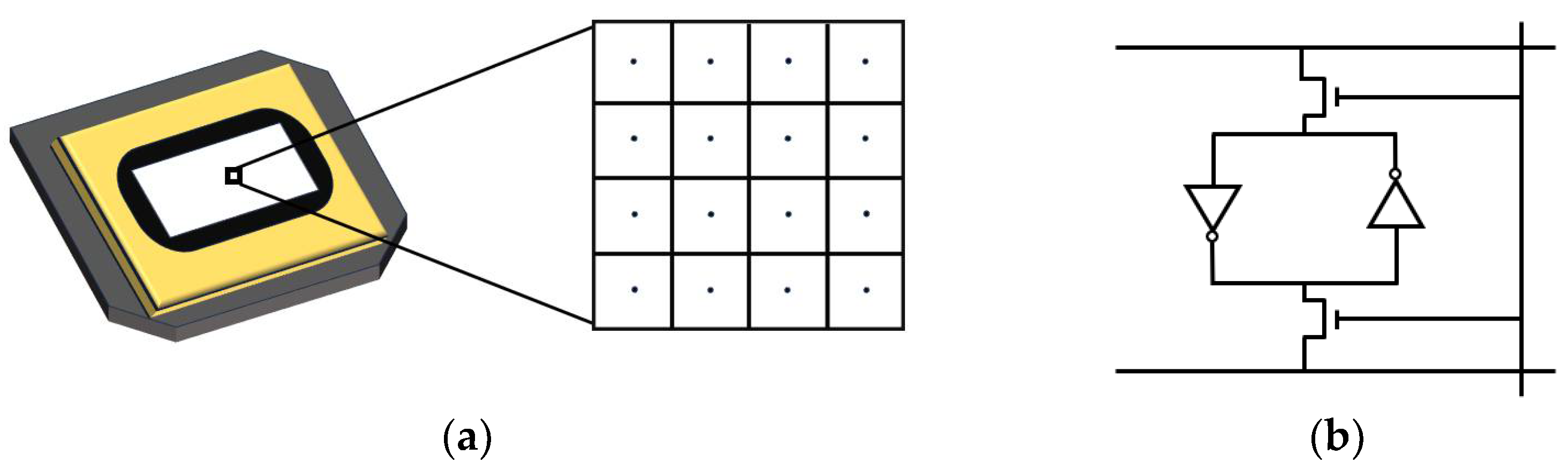
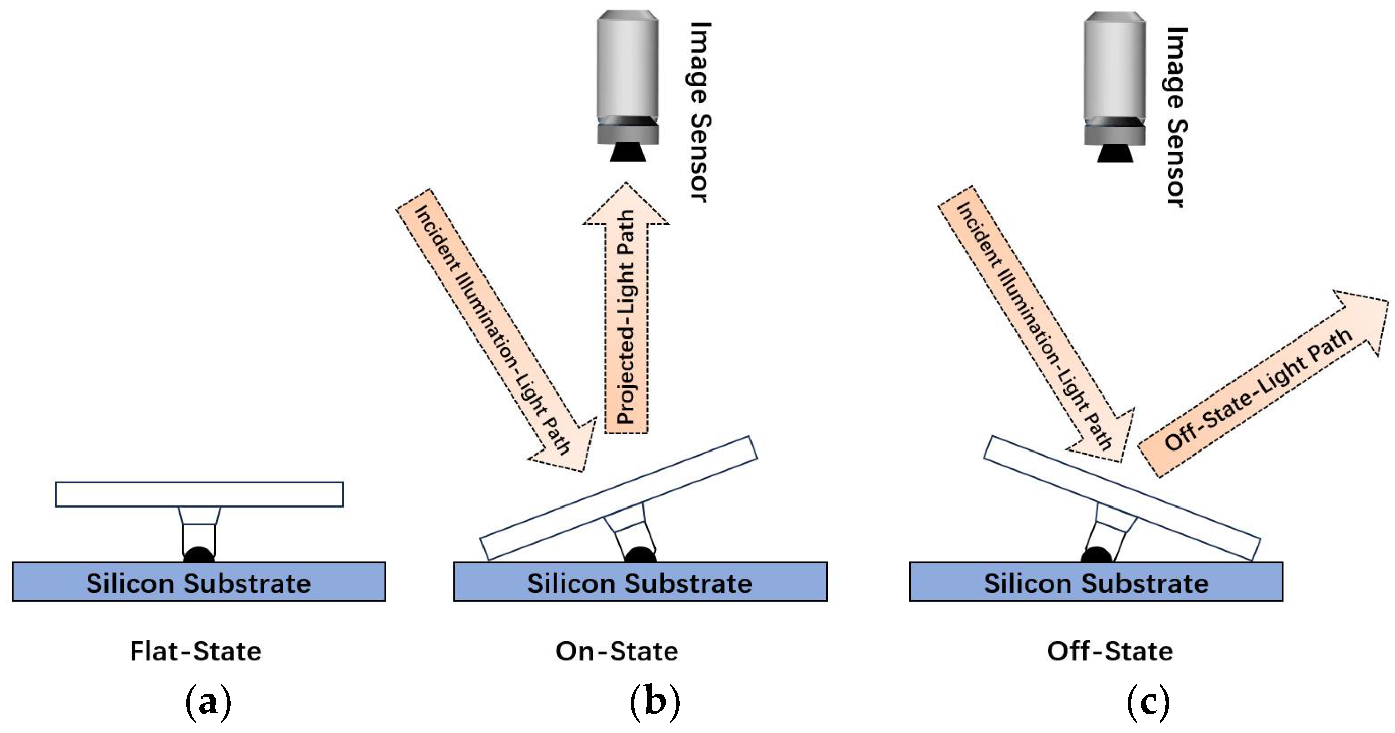
2.1. Basic Working Principle of DMD

The appearance of a DMD chip and its surface micromirror array are shown in Figure 1. Each micromirror has a one-bit CMOS storage unit for storing the current position status information of the micromirror.
When the data stored in the storage unit equal 1, the micromirror at this position will be set to “on”; otherwise, it will be set to “off”. The flipping process of DMD micromirrors is shown in Figure 2. When the micromirror is in the “on state”, it will deflect forward by 12 degrees under the action of electrostatic force, and the light reflected by the micromirror from the light source will be collected by the image sensor. When the micromirror is in the “off state”, it will reverse by 12 degrees, and the reflected light will not reach the image sensor. When the micromirror is in a “flat state” (Figure 2a), it is in a free-movement state and does not function during the projection process [22].

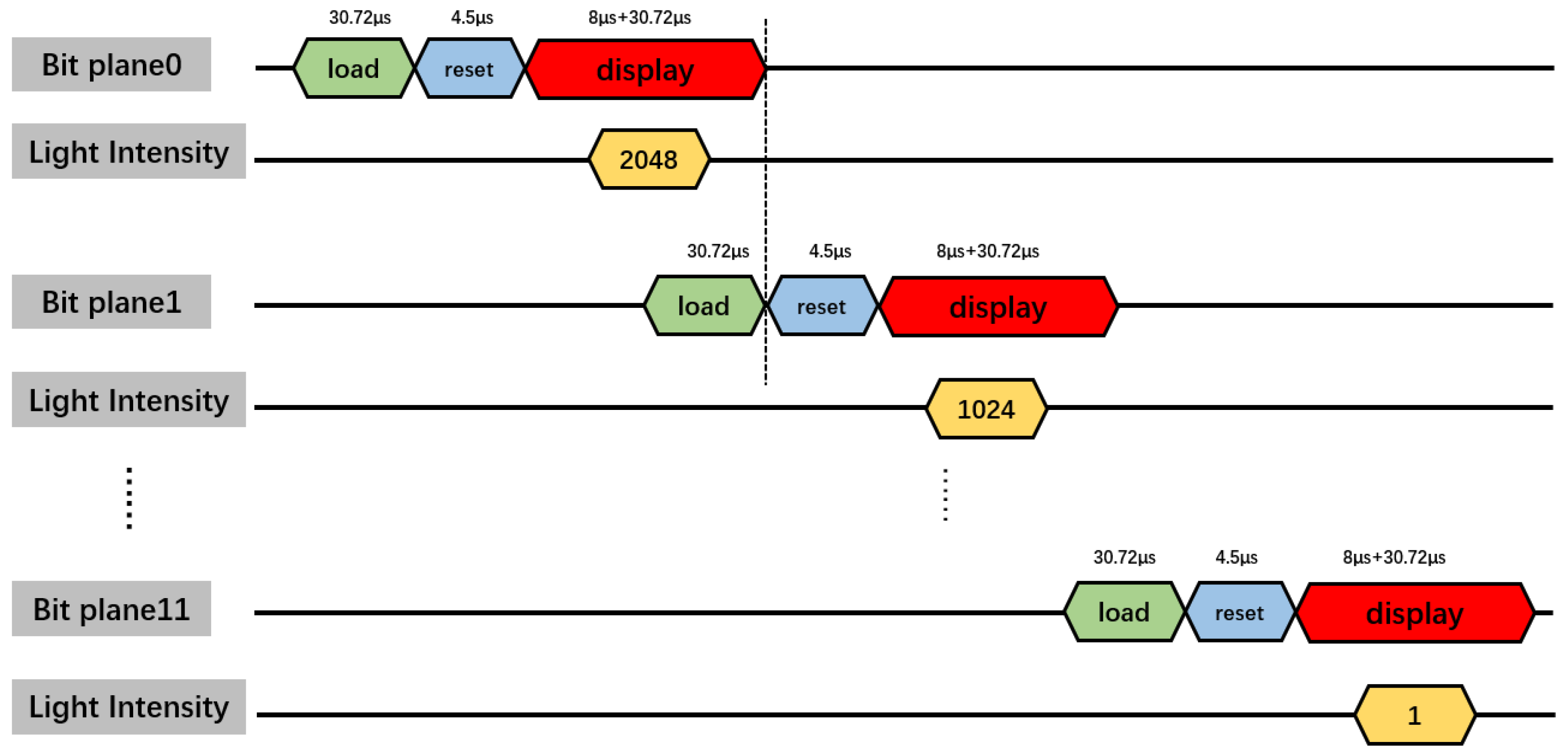
2.2. Bit Plane Decomposition

The bit plane decomposition of grayscale images refers to converting the decimal form grayscale value of each pixel in the grayscale image into binary and then extracting each bit of the binary form grayscale value separately to form a new image. As shown in Figure 3, a four-bit grayscale image is first binarized, and then, the binarized image is split into four-bit planes. In the DMD grayscale modulation process, the first step is to decompose the image data into bit planes and then project the bit planes separately. The decomposed different bit planes will be directly used as data for CMOS storage units, providing flip information to the micromirror equivalent to dividing a four-bit grayscale image into four binary images. After displaying different planes at different time periods, the original grayscale image can be restored by the image sensor [23].

2.3. Traditional DMD Grayscale Modulation

The most commonly used modulation method for traditional DMD projection grayscale images is pulse width modulation (PWM). By changing the opening and closing time of a single micromirror, it can project a grayscale image. The PWM corresponds to different bit planes of grayscale images in different time regions. The duration corresponding to the most significant bit (MSB) of an image is the longest, while the duration corresponding to the least significant bit (LSB) is the shortest. Each bit plane will be arranged in order of weight [24,25]. The timing diagram of projecting a four-bit grayscale image using PWM is shown in Figure 4. This timing diagram describes the PWM process of a single pixel in DMD. The projected grayscale value is 10. First, convert it to binary form “1010” to obtain the states that the micromirror should be in four bit planes, namely, “off”, “on”, “off”, and “on” (from bit plane 0 to bit plane 3). The duration from bit plane 0 to bit plane 3 is multiplied in sequence, namely, t, 2 t, 4 t, and 8 t. And t is the holding time of the minimum bit plane of the DMD micromirror. In this way, the DMD micromirror completes a single-pixel projection of a four-bit grayscale image with a grayscale value of 10. By providing working timing and voltage signals through the DMD driver board, the DMD micromirror array can project a grayscale image.
In the process of traditional PWM projection of grayscale images, the power of the illumination light source remains unchanged. Grayscale images are generated solely through the timing control of a single DMD. Below is a theoretical modeling and formula description of the imaging mechanism of this method.
In a typical DMD projection system, if the optical power density of the incident light source is denoted as EOT, and the area of a single micromirror is denoted as S, the optical power that is reflected from the surface of each micromirror per unit of time can be expressed as follows:
P T ( u , v ) = E O T S
where (u, v) is the coordinate of a single micromirror on the DMD surface.
In this method, the projected image is divided into a number of bit planes, and the DMD projects the energy of each bit plane sequentially to a specified region in space through the reflection of the micromirrors. The stabilization time of each bit plane is multiplied sequentially to project a grayscale image. The display time of the smallest bit plane is set to t, and the display time of the bit plane m is set to 2mt, where m is a consecutive integer ranging from 0 to n − 1, and n is the number of quantization bits of the projected image. Let the magnification of the projection system be β, and the transmittance be θ. The spatial energy distribution of a frame of the image projected from the specified projection area in the specified time can be described by the following equation:
W ( u , v ) = m = 0 n 1 P T ( u , v ) β θ 2 m t α m ( u , v )
where αm(u, v) is the micromirror state of the (u, v) coordinate DMD when the m bit plane is projected. When this micromirror is open, the state is valid and takes a value of 1; when closed, the state is invalid and takes a value of 0. The meaning of Equation (2) is that the spatial energy distribution of a specified projection area is the sum of the output optical power of each micromirror multiplied by the duration of different bit planes, system parameters, and the micromirror state. In the given equation, the system’s adjustable parameters are constrained by the duration of 2mt for each bit plane. Considering the projection of an eight-bit grayscale image as a scenario, once the minimum display time “t” for the lowest bit plane is determined, the maximum display time for the highest bit plane would be 128t. This significantly increases the total time required to project a single frame of the image. Moreover, in situations where the integration time T of the image sensor is fixed, the achievable grayscale levels in the displayed image will be restricted to a limited range.

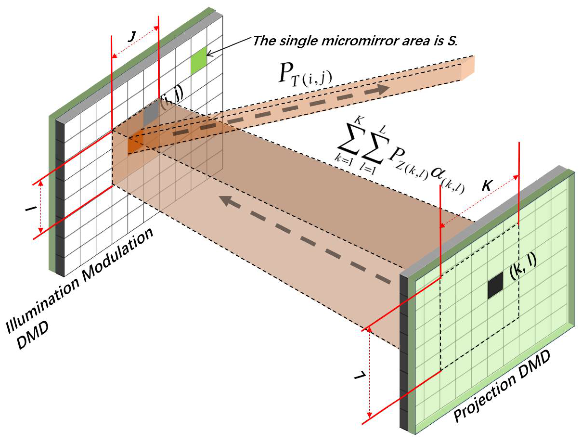
2.4. Dual DMD Synchronous Modulation

In the image sensor test, the frame period of a test image should be less than the integration time of the image detector. Let the integration time of the camera under testing be T. In the actual projection process, the following should be satisfied:
m = 0 n 1 2 m t T
For a specific model of DMD, the minimum bit plane duration is affected by the micromirror flip time, stabilization time, and other factors. Therefore, there is a minimum value limitation, which should satisfy ttmin. By combining T and tmin, the maximum value of n can be determined. By taking a 0.7XGA-type DMD as an example, the minimum value of the minimum bit plane stabilization time is 8 μs [26], and, under the condition that the camera integration time is 1 ms, the maximum value of n can be calculated to be 7. With the rapid development of imaging technology, mainstream high-end image sensors have reached high quantization bits [27,28]. It is clear that the number of projection quantization bits of traditional grayscale modulation cannot be met by the test demand, and image sensor test technology has encountered a significant bottleneck.
In the traditional DMD projection system, when the frame period of the projected image is fixed, the bit number of the projected image cannot be improved, and the frame period must be extended when a higher bit number of the image is desired to be projected. To solve this contradiction, in this paper, a dual DMD-based grayscale modulation scheme is proposed. In Equation (2), it is easy to see that, in the case where the total area of projection area A, magnification β, and transmittance θ are all fixed, the spatial energy distribution W(u, v) in the projection area is affected by not only the projection bit plane retention time factor 2mt but also the optical power reflected from each micromirror PT(u, v) per unit time. Traditional DMD-based grayscale projection systems generally design PT(u, v) as a constant, and the number of quantization bits of the projection system can be significantly improved if PT(u, v) is quantized synchronously. In an actual design, another DMD can be used to modulate PT(u, v). If the optical power density incident to the illumination modulation DMD is EOZ, and the area of a single micromirror is S, then the optical power emitted from the surface of a single micromirror of the illumination modulation DMD is
P Z ( k , l ) = E O Z S
where (k, l) is the coordinate of a single micromirror on the DMD surface.
Through the design of the optical system, the illumination can be controlled to modulate the light-through area of the DMD, thus achieving the modulation of the optical power density EOT on the surface of the projection DMD and, thus, the modulation of PT. This process can be described by using the following equation:
P T ( i , j ) = k = 1 K l = 1 L P Z ( k , l ) α ( k , l ) I J · S · S = k = 1 K l = 1 L P Z ( k , l ) α ( k , l ) I J
where K and L are the number of rows and columns of the effective intensity modulation region of the illumination modulation DMD; I and J are the number of rows and columns of the effective imaging region of the projection DMD; (k, l) and (i, j) are the coordinates of the micromirrors on the illumination modulation DMD and projection DMD, respectively, and α(k, l) is the state of the DMD micromirror in (k, l) coordinates, which is valid when this micromirror is turned on with a value of 1 and invalid when it is turned off with a value of 0. Equation (5) describes the process of calculating the optical power PT(i, j) emitted by each micromirror of the projection DMD by the optical power PZ(k, l) emitted by each micromirror of the illumination modulation DMD. This process is shown in Figure 5. As shown in Figure 5, the meaning of k = 1 K l = 1 L P Z ( k , l ) α ( k , l ) is the total light power emitted by the illumination modulation DMD. Assuming that the projection area of the projection DMD is rectangular, I and J are the numbers of rows and columns in the effective imaging area of the DMD. S is the area of a single micromirror. The meaning of IJ · S is the total area of the projection region. The equation k = 1 K l = 1 L P Z ( k , l ) α ( k , l ) I J · S represents the optical power density incident on the projection DMD. Multiplying by S represents the optical power reflected by a single micromirror of the projection DMD.
As can be seen in Equation (5), the denominator is the total number of micromirrors in the effective imaging area of the projection DMD. After the design of the optical system, the area of the illumination modulation DMD outgoing light arriving at the projection DMD can be kept unchanged, and the only thing that changes is the optical power. Then, theoretically, by changing the difference in the number of micromirrors turned on in each bit plane of the illumination modulation DMD, it is possible to perform the quantization of PT(i, j) in steps of 1 for 0-K × L levels. 0-K × L refers to the number of micromirrors that can be turned on by the illumination modulation DMD in the effective illumination area, which can vary from 0 to K × L. However, in an actual system design, considering the feasibility of the project, PT(i, j) is quantified as an exponent of 2 for K × L. Then, Equation (5) can be expressed as
P T ( i , j ) = 2 h P z
where PZ is the minimum quantized optical power of the illumination modulation DMD, and h is the quantized level of its outgoing optical power.
By integrating the above derivation process, the spatial energy distribution W(i j) in a specified projection region for a specified time under dual DMD modulation can be described as the following equation:
W ( i , j ) = m = 0 n 1 2 h P Z β θ 2 m t α m ( i , j )
The meaning of this equation is that the spatial energy distribution W(i, j) of the dual DMD modulation scheme incident on the image detector is equal to the product of the optical power emitted by each micromirror of the projection DMD multiplied by the system parameters, bit planes duration, and the micromirror state. The equation above shows that the spatial energy distribution of a specified area can be modulated in two dimensions through the use of an optical system with a specified total area A, magnification β, transmittance θ, and opening and closing states αm(i, j) of each micromirror. This modulation occurs through the manipulation of the optical power reflected by each micromirror of the projection DMD and the duration of each bit plane, representing energy- and time-domain modulation in the process of modulating a grayscale image. By calculating the number of quantization bits required to project a frame and by considering the integration time T of the image sensor, the system’s quantization level n, and the quantization level h of the emitted optical power of the illumination modulation DMD, we can achieve a final quantization level of n × h by adjusting the duration of each bit plane. This approach significantly improves the quantization level compared to traditional modulation methods. Through the double modulation of the emitted optical power and the duration of each bit plane by the illumination modulation DMD, the total duration of each image frame can be reduced, leading to an effective improvement in the frame frequency of the displayed grayscale images.

3. Materials and Methods

3.1. Projection Experiment Protocol

On the basis of traditional pulse–width grayscale modulation, two DMDs are used to modulate the time and energy domains of the projected image simultaneously. The grayscale image of the designed system is projected as 12 bits; the display time of each bit plane of the projection DMD is the same as that of the smallest bit plane, t. The number of micromirrors opened in the illumination modulation DMD is halved, in turn, from bit plane 12 to bit plane 1, and its optical power is halved, in turn. In each cycle of action of the projection DMD and the illumination modulation DMD, the projection DMD projects each bit plane of the 12-bit grayscale image, and the illumination modulation DMD performs light source intensity modulation for a total of 12 times. Then, under this scheme, the spatial energy distribution of the specified projection region can be obtained from Equation (7) as follows:
W ( i , j ) = m = 0 11 2 h P Z β θ t α m ( i , j )
where h is an integer from 0 to 11.
The control system for the two digital micromirror devices (DMDs) and their interactions with the main control computer are illustrated in Figure 6. The main control computer and the projection DMD communicate via a 10 Gigabit network port for image data transmission, while the main control computer and the main control Field Programmable Gate Array (FPGA) use RS422 to send commands. The main control FPGA receives commands from the main control computer and sends trigger signals to both the galvanometer and projection DMD. The projection DMD, in turn, sends trigger signals to the illumination modulation DMD each time the projection begins. The illumination modulation DMD stays in synchronization with the projection DMD to modulate the intensity of the light source. Ultimately, a 12-bit grayscale image is projected onto the target surface image sensor for imaging.
In the dual DMD synchronous modulation experiments conducted through the image sensor to obtain the grayscale image generated by the system, it is essential for the target camera to be mounted onto a high-precision displacement stage. This setup is crucial for meeting the requirements for receiving a larger field-of-view image. For the DMD drive platform, TI’s DLP7000 (Texas Instruments, Dallas, TX, USA) suite is chosen, which is part of the DiscoveryTM4100 platform (Texas Instruments, Dallas, TX, USA). The DLP7000 chipset within the DiscoveryTM4100 platform enables high-resolution and high-performance spatial illumination modulation. It currently boasts the fastest pattern rate among DLP products [22]. The main control computer is responsible for transferring image data and control instructions to the system. The image data format that the DMD can read is the raw format. By utilizing software tools to create images in the specified format and resolution, the image data can then be transmitted to the DMD through a 10 Gigabit Ethernet port using the upper computer software.
A schematic diagram of the experimental system is presented in Figure 7. The laser is used as a light source. The wavelength of the laser is 532 nm, and the power is 100 mW. The diffuser is a motor with sulfuric acid paper used to eliminate laser speckles. The illumination optical system provides illumination for the entire system. The light beam enters the collimator after being reflected by two DMDs. The function of a collimator is to convert a beam of light into parallel light. The two-dimensional galvanometer reflects the light beam. The use of the two-dimensional galvanometer is for the convenience of system assembly and subsequent experimental expansion. Its main function is to reflect light. The imaging objective converges the light beam and projects it onto the image sensor for imaging. The image sensor used in the experiment is an industrial camera. Its resolution is 6576 × 4940. The pixel depth is 12 bits. The pixel size is 3.2 um. Its spectrum is black and white. The image sensor is mounted on a displacement table. The displacement table can move in a two-dimensional plane, which is more convenient for the camera to receive images.

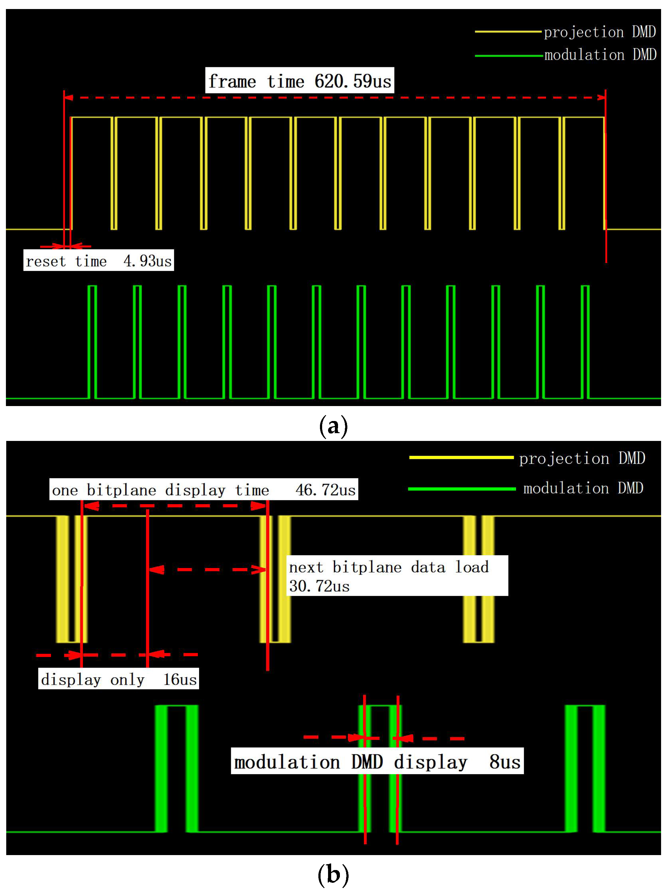
3.2. Frame Rate Calculation

The experimental system used is a 0.7XGA-type DMD, with a resolution of 1024 × 768. The system’s maximum clock frequency is 400 Mhz, and the data bus bit width is 32 bits. In each clock jump edge, data are loaded. Thus, the clock cycle required to load one line of data is T = 1 2 × ( 1024 32 ) = 16 clock cycles; loading a line of time takes t 1 = 16 × 1 4 × 10 8 = 0.04 μs, and loading the whole image takes t 2 = 768 × 0.04 = 30.72 μs.
Figure 8 shows the pulse–width modulation principle of a 0.7XGA-type DMD displaying a 12-bit grayscale image. The time required to load image data for each bit plane is 30.72 μs. The reset time is 4.5 μs [26], and the display time is 38.72 μs. The scheme does not use a block-clearing instruction but, instead, loads the data of the next bit plane at the same time as displaying the previous bit plane, which can effectively reduce the engineering complexity and improve the frame rate.
Based on this figure, the theoretical minimum time for a DMD to display a 12-bit grayscale image can be calculated as follows:
T P = T r + T d + T l = 12 × ( 4.5 + 8 + 30.72 ) = 518.64   μ s
Frame rate conversion is as follows:
F p = 1 / T p 1928.12   hz
In the context of the frame display, Tp represents one frame’s display period; Tr denotes the total reset time; Td stands for the total display time, and Tl signifies the total data loading time. Additionally, Fp represents the display frame frequency. Through the utilization of dual DMD synchronous modulation, it becomes evident that the frame frequency for displaying high-gray-level images can be significantly increased to achieve high-level performance.
In the actual engineering implementation, it is necessary to allow some time for the DMD micromirror to stabilize after each reset. This means that a waiting period is required after the reset of the projection DMD before resetting the illumination modulation DMD. Additionally, in order to ensure stable imaging, it is important to reset the illumination modulation DMD only after the image from the projection DMD has been fully displayed. The reset time for the DMD micromirror is slightly longer than 4.5 μs. If the illumination modulation DMD is reset immediately after the projection DMD, then there will be a risk of cumulative errors from different bit planes, causing the display of later bits to be out of order. Therefore, the reset times of the two DMDs are staggered.
The shortest display time for a DMD micromirror is 8 μs in practical implementation. The display time for the illumination modulation DMD can reach 8 μs because its image is generated by the field programmable gate array (FPGA) on the DMD driver board itself, eliminating the need for image data uploading and downloading. In contrast, the image data for the projection DMD are transmitted from the main control computer through a 10 Gigabit Ethernet port to DDR3 and then written into the FPGA before being transmitted to the DMD micromirror array. Due to the fast reaction speed of DMD micromirrors, they must wait for data transmission before resetting, resulting in the minimum display time of the projection DMD being more than 8μs. Therefore, the theoretical calculations of timing diagrams should be used as a reference only, and actual frame rates can be obtained from the triggering waveforms of the projection and illumination modulation DMDs.

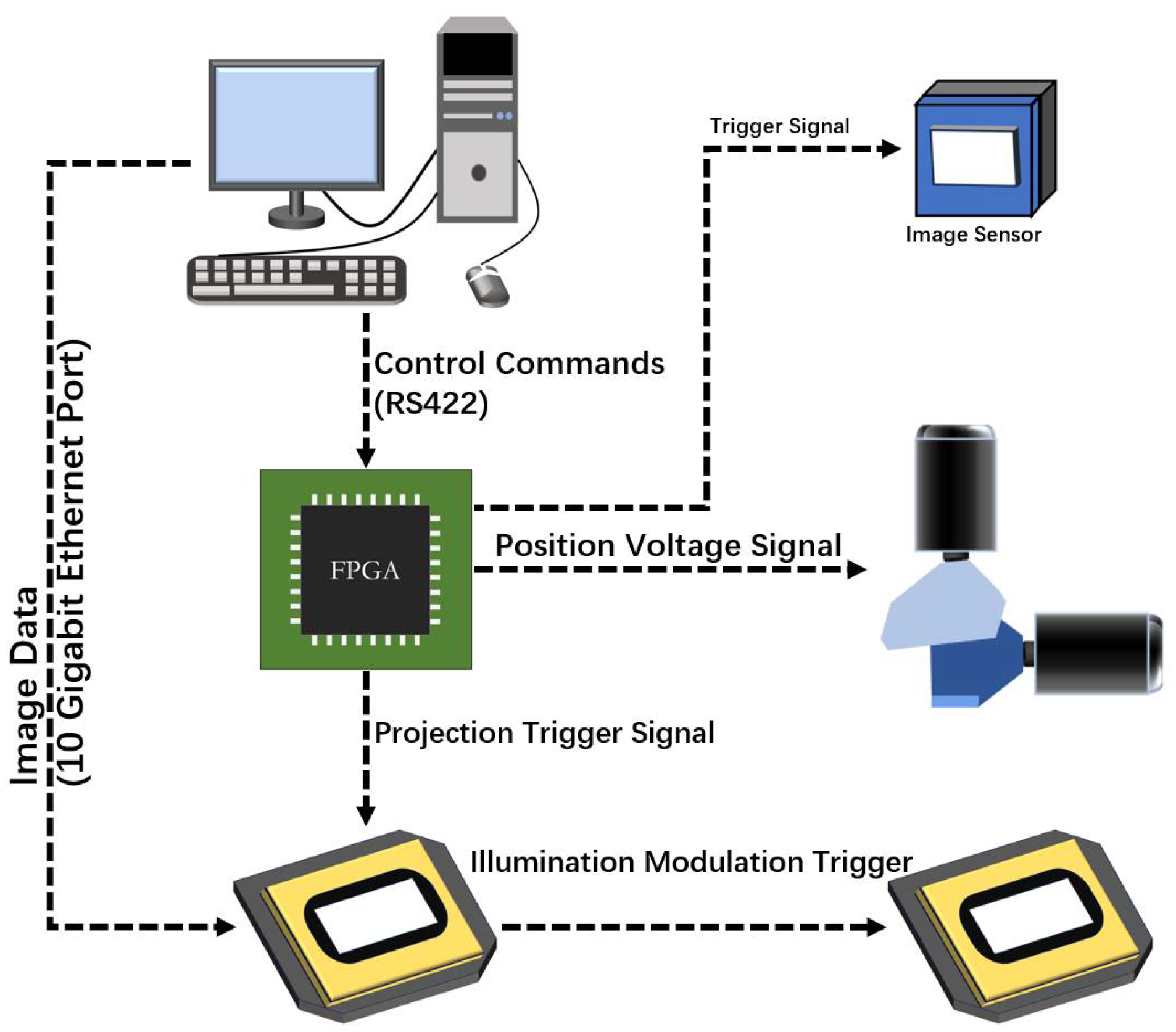
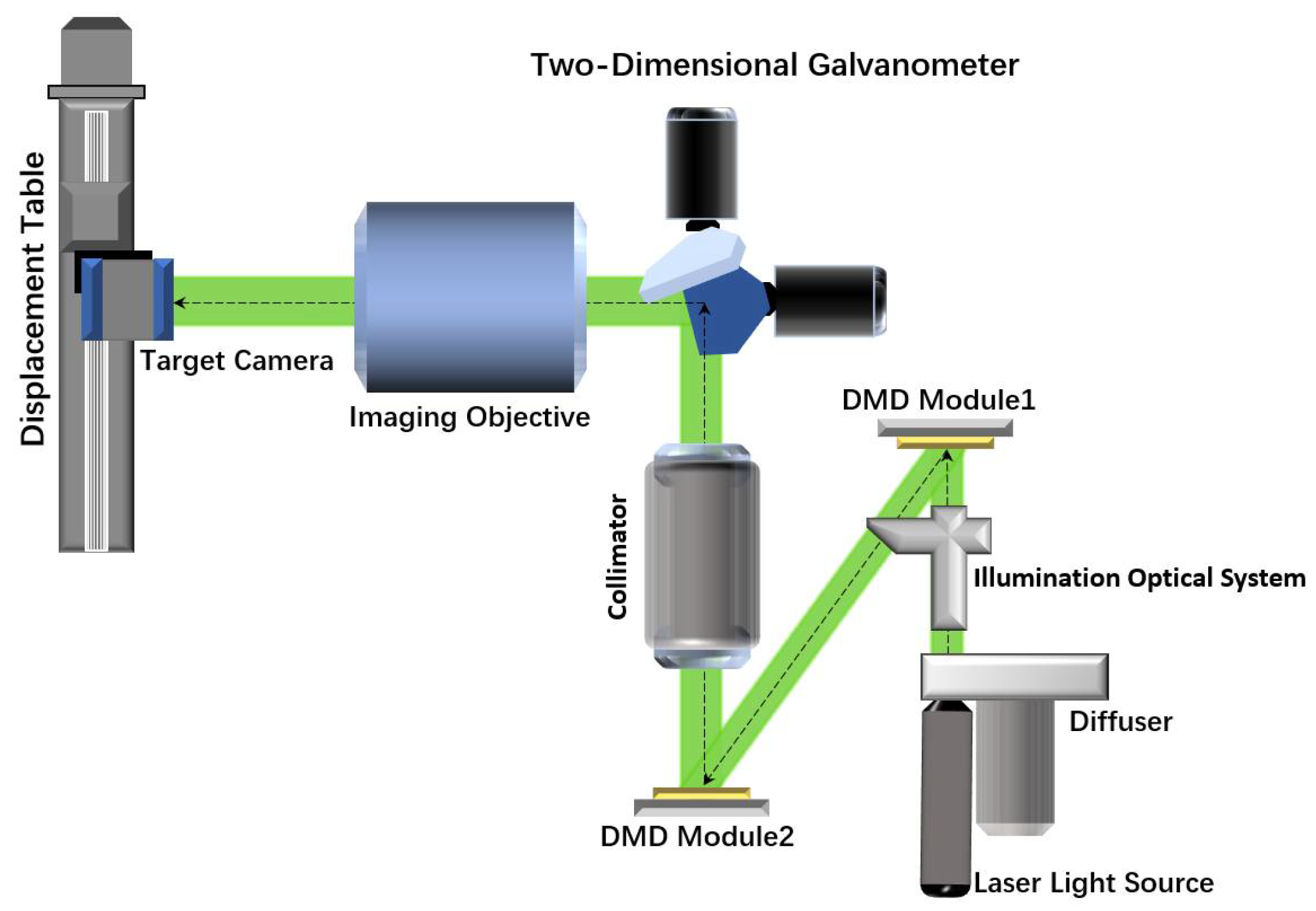
3.3. Experimental System Construction

The experimental device was built on the principle of dual DMD synchronous modulation. The device includes DMD modules, a light source, a parallel light tube, an imaging objective lens, a cast reflector, and other components, as depicted in Figure 9. The light source is illuminated by a laser Kohler. When installing the two DMDs, it is necessary to ensure the parallelism of the DMD chip surface. The installation angle error is within ± 0.1°. Due to the projection image being only on one area of the DMD, the horizontal unidirectional error of the two DMD chip supports is within ± 1 mm. This experimental setup offers multiple modulation dimensions, enabling the verification of various influencing factors.

4. Results and Discussion

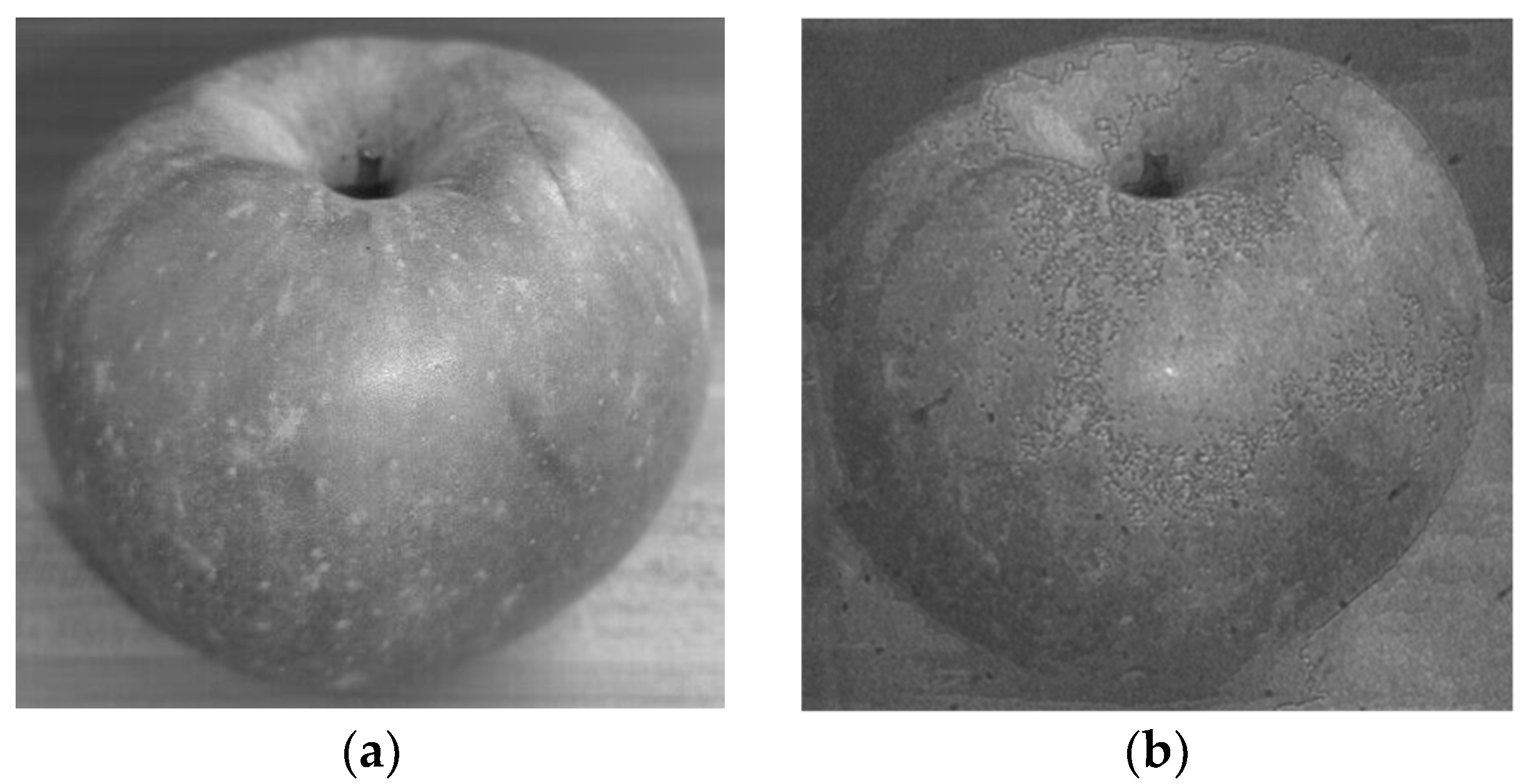
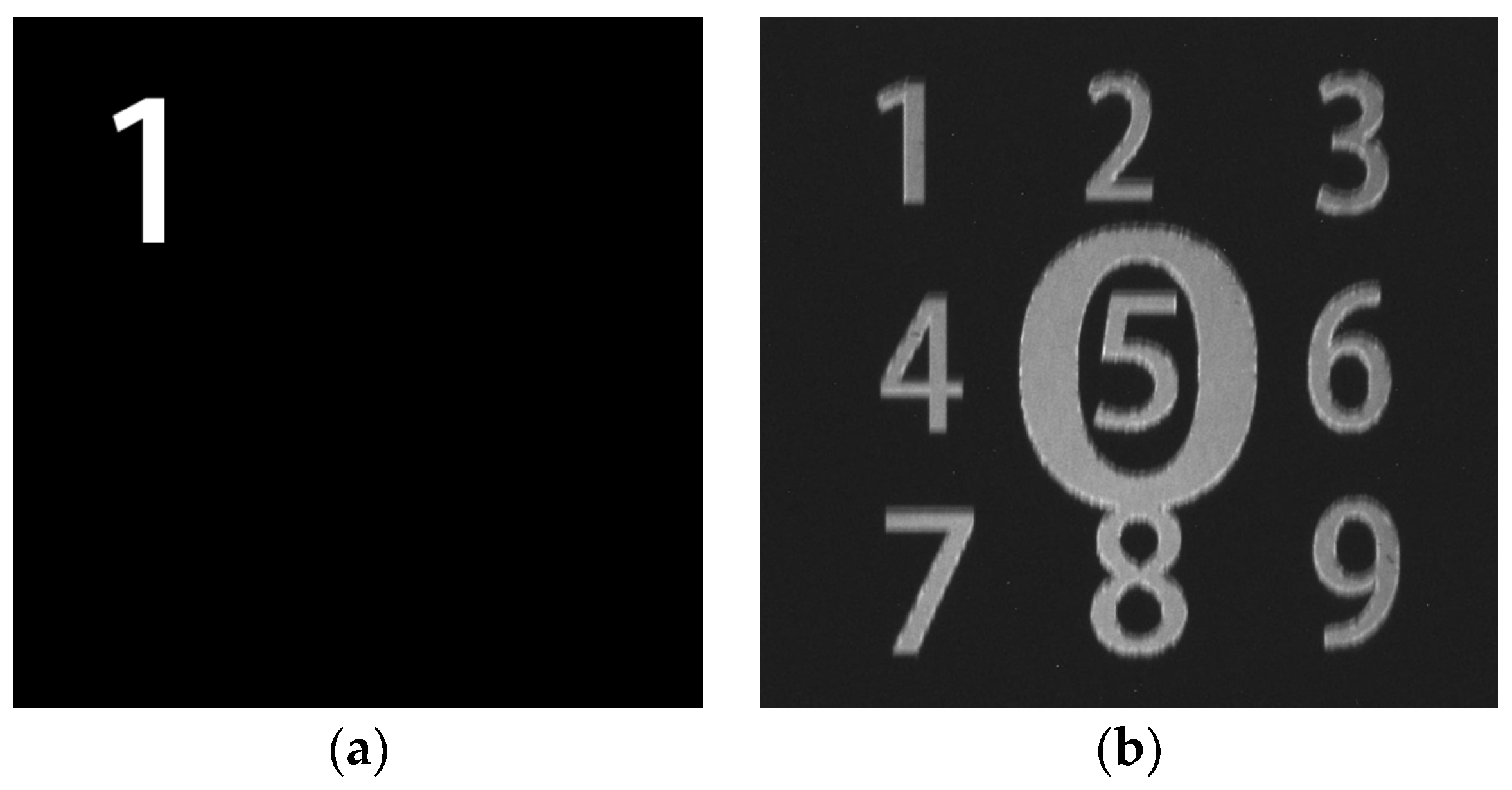
4.1. Landscape Projection Test

As demonstrated in Figure 10, the “apple” physical image and system image projections display excellent imaging quality. The details of the original picture are accurately and completely reflected, showcasing the system’s ability to reproduce intricate details effectively.
Use root mean square error (RMSE), peak signal-to-noise ratio (PSNR), and structural similarity index (SSIM) to evaluate the similarity between two images. RMSE refers to the square root of the average difference in grayscale values between two corresponding pixels in an image. The smaller the value, the more similar the two images are. PSNR is an indicator of image quality, representing the ratio of peak signal to noise in an image. The larger the value, the more similar the two images are. SSIM considers brightness, contrast, and structural information, and the closer the value is to 1, the more similar the two images are. Three values were calculated through the program and are shown in Table 1. Based on the analysis of three data points, it can be concluded that the two images are quite similar.

4.2. Experimental Verification

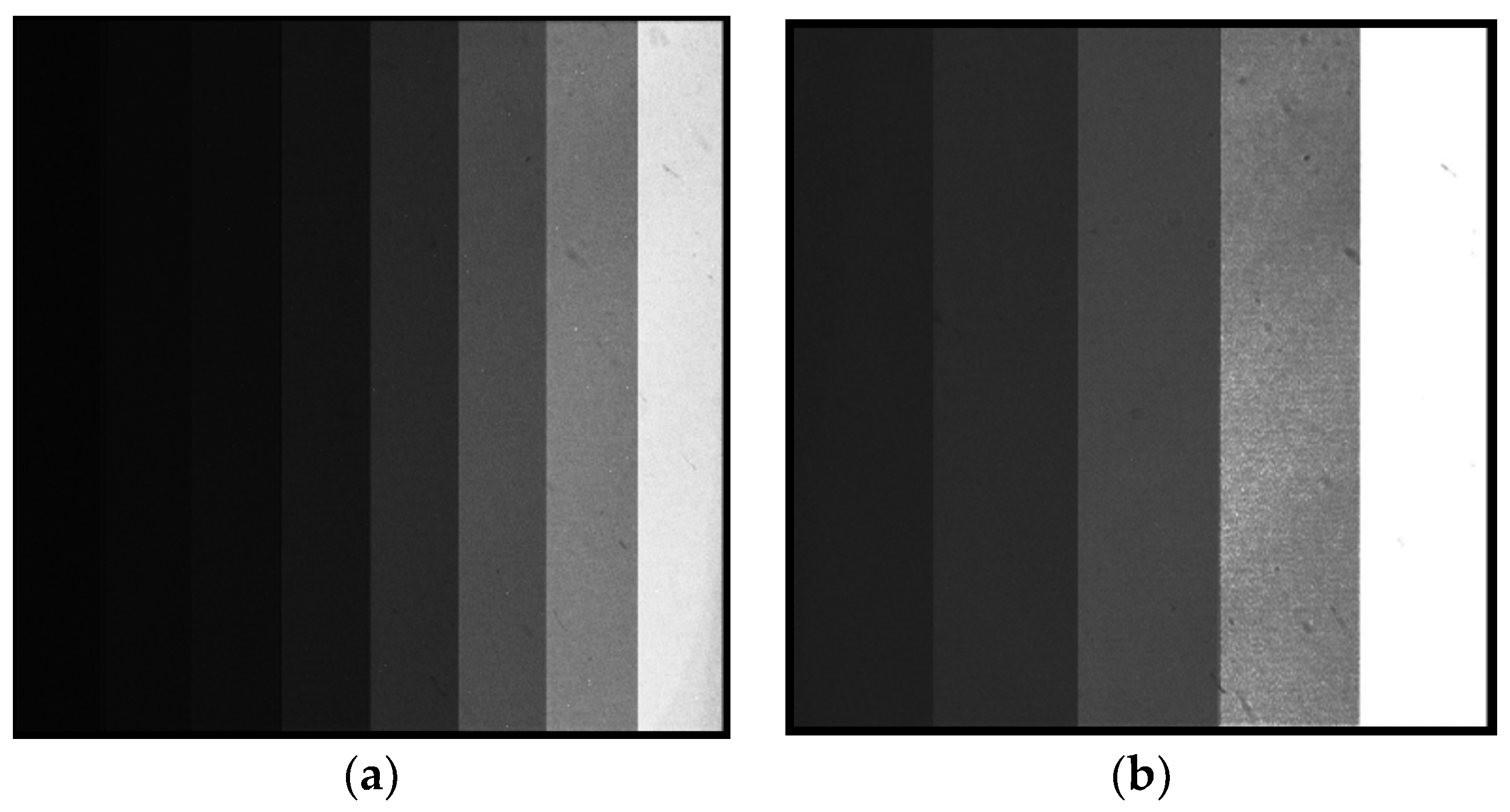
4.2.1. Grayscale Test

A gray-level test image was projected, containing regions with different gray values, in order to determine whether the image sensor can distinguish the gray level changes in the different regions. If the sensor was able to detect these changes, it would indicate that the gray level of the projected image met the predefined target. To enhance the visibility of the grayscale changes, the 1- to 12-bit grayscale was divided into two stages for projection. The first stage projected a test image with 1 to 8 grayscale levels, while the second stage projected a test image with 8 to 12 grayscale levels. The test images were generated using programs, and the resulting images received by the two-stage target surface camera are shown in Figure 11. The gray values of the different gray-level regions in the projected images of the two stages were averaged separately to establish the correspondence between the gray values of the original image and the projected image, as shown in Table 2.
By taking the gray values of the eight-bit grayscale image as the point of articulation, the two sets of test data are drawn simultaneously in a coordinate system with logarithmically scaled horizontal and vertical coordinates, and the gray level correspondence is shown in Figure 12. Here, the x-axis of the horizontal coordinate represents the gray level of the original image, while the vertical axis (G) represents the gray value of the projected image. It can be observed in the constructed coordinate system that the correspondence between the gray values of the original image and the projected image is approximately linear, indicating that the image sensor is capable of distinguishing the gray level changes in the projected image, with the gray level of the projected image reaching 12 bits.

4.2.2. Frame Rate Test

To measure the frame frequency captured by the image sensor, an oscilloscope can be utilized to analyze the trigger waveforms of the target projection DMD and illumination modulation DMD. As illustrated in Figure 13, the yellow waveform represents the projection DMD, while the green waveform corresponds to the illumination modulation DMD. The high level indicates the duration of the projection of the DMD micromirror after the flipping process is complete. After redrawing the waveform of the oscilloscope, by analyzing the waveform diagrams, it can be determined that the actual projected frame period of an image is 620.59 microseconds, resulting in a frame rate of 1611.37 Hz. A discrepancy of approximately 300 Hz is observed when compared with the theoretical calculation.
The second waveform depicted in Figure 13 provides a detailed overview of the waveforms associated with the projection DMD and the illumination modulation DMD. By addressing the issue highlighted at the conclusion of Section 3.2, the actual minimum display time of the projection DMD can be extrapolated from the waveforms, revealing it to be approximately 16 microseconds. This extended display time allows the previous bit to remain illuminated for 30.72 microseconds after the data loading of the subsequent bit without disrupting the overall operational timing. This modification not only enhances the brightness of the final projected image but also alters the flexibility in adjusting the system design.
Experimental verification of the projected frame rate can be conducted by a test pattern comprising numbers from 0 to 9, similar to the example shown in Figure 14a, which depicts the number 1 pattern. The number patterns in the ten images are distributed in different positions. After projecting a total of ten test images containing patterns 0–9, the stacked test image in Figure 14b can be obtained. The test pattern is projected onto the image sensor, and the capture frame rate of the target camera is configured accordingly. The projection time of the ten images can be obtained from the trigger waveform of DMDs mentioned earlier. Considering system errors, the integration time of the image sensor is set to be slightly greater than the projection time of the ten images. In the external triggering mode, the image sensor and two DMDs will work synchronously under the action of the external triggering signal. If the digital patterns from 0 to 9 can be imaged, it indicates that all 10 images have been imaged within the integration time, and the projection frame rate has reached the predetermined target. When conducting the experiment, the integration time of the image sensor was set to 6500 μs (slightly greater than 620.59 μs × 10). After starting the projection, the image sensor captured the image in Figure 14b. This indicates that the projection frame rate has reached at least 1538 Hz ( 10 6 × 6500 10 ) . The system’s projection frame rate has basically met the expected requirements.

4.3. Discussion

This study successfully designed and validated a high-frame-frequency and large-grayscale simulation projection system based on digital micromirror devices, with significant application potential in the field of image sensor testing. The innovation of this study lies in the use of a dual DMD synchronous modulation scheme, which greatly improves the frame frequency and gray level of the system through dual modulation in the time and energy domains. This scheme, compared with conventional single DMD projection systems, achieves high-frame-rate projection while maintaining high gray levels, which is crucial for capturing and simulating high-speed dynamic scenes. However, it was observed that the brightness of the final image decreased when the display time of each bit plane was short. Future work should focus on optimizing the system design to achieve higher brightness and contrast while maintaining a high-frame rate and gray level. Despite the positive results, there are limitations that need to be addressed, such as testing the stability and reliability of the system under a wider range of conditions and researching adaptability to different types of image sensors in order to ensure the system’s versatility and flexibility.

5. Conclusions

After studying the working principle of digital micromirror devices, a novel high-frame-frequency and large-grayscale simulation projection scheme was proposed, aiming to address the limitations of pulse–width grayscale modulation in achieving higher grayscale levels in a limited detector integration time. The system design involved using one DMD to modulate the light intensity of the light source and another DMD for image projection. Theoretical calculations and an experimental verification demonstrated that the system could achieve a frame rate of 1611.37 Hz when projecting 12-bit grayscale images, meeting the desired performance goals and providing valuable technical support for image sensor testing. The potential application of this design in the field of image sensor testing requires further exploration, including adapting existing test processes, optimizing system performance, and integrating with existing technologies. This presents a challenging yet promising area for future research and development.

Author Contributions

Conceptualization, L.M., J.L. and Y.Y.; methodology, L.M.; software, H.L.; validation, L.M. and Y.Y.; formal analysis, J.L. and Y.T.; investigation, Z.L.; resources, Y.Q.; data curation, L.M.; writing—original draft preparation, L.M.; writing—review and editing, L.M.; visualization, M.Z.; supervision, J.L.; project administration, J.L.; funding acquisition, J.L. All authors have read and agreed to the published version of the manuscript.

Funding

This research was funded by the Jilin Provincial Institute of Science and Technology Innovation Technology Collaborative Innovation Project, grant number 20240207009CX.

Institutional Review Board Statement

Not applicable.

Informed Consent Statement

Not applicable.

Data Availability Statement

The data included in this experiment are not yet publicly available but can be obtained from the author upon reasonable request.

Conflicts of Interest

The authors declare no conflicts of interest.

References

  1. Introduction to ±12 Degree Orthogonal Digital Micromirror Devices (DMDs). Available online: https://www.ti.com/lit/pdf/dlpa008?keyMatch=DMD&tisearch=search-everything (accessed on 16 April 2024).
  2. Cheng, Z.; Toshiyoshi, H. CMOS-MEMS Micro-Mirror Arrays by Post-Processing ASMC 0.35-μm CMOS Chips. J. Microelectromech. Syst. 2017, 26, 1435–1441. [Google Scholar] [CrossRef]
  3. Gong, C.; Hogan, T. CMOS compatible fabrication processes for the digital micromirror device. IEEE J. Electron. Devi. 2014, 2, 27–32. [Google Scholar] [CrossRef]
  4. Wang, J.; Huffman, J.; Pinheiro, P.; Hall, J. An embedded reset driver for digital micromirror devices (DMDs). J. Soc. Inf. Disp. 2010, 18, 868–872. [Google Scholar] [CrossRef]
  5. Yu, W.-K.; Yang, Y.; Liu, J.-R.; Wei, N.; Wang, S.-F. Secondary Complementary Balancing Compressive Imaging with a Free-Space Balanced Amplified Photodetector. Sensors 2022, 22, 3801. [Google Scholar] [CrossRef]
  6. Zhang, X.; Xie, J.; Li, C.; Xu, R.; Zhang, Y.; Liu, S.; Wang, J. MEMS-based super-resolution remote sensing system using compressive sensing. Opt. Commun. 2018, 426, 410–417. [Google Scholar] [CrossRef]
  7. Li, D.; Wei, H.; Fang, H.; Gao, Y. Group Control of Photo-Responsive Colloidal Motors with a Structured Light Field. Photonics 2024, 11, 421. [Google Scholar] [CrossRef]
  8. Kang, E.; Choi, H.; Hellman, B.; Rodriguez, J.; Smith, B.; Deng, X.; Liu, P.; Lee, T.L.-T.; Evans, E.; Hong, Y.; et al. All-MEMS Lidar Using Hybrid Optical Architecture with Digital Micromirror Devices and a 2D-MEMS Mirror. Micromachines 2022, 13, 1444. [Google Scholar] [CrossRef]
  9. Dudley, D.; Duncan, W.; Slaughter, J. Emerging digital micromirror device (DMD) applications. In Proceedings of the MOEMS Display and Imaging Systems, San Jose, CA, USA, 28–29 January 2003. [Google Scholar]
  10. Zhu, L.; Cao, Z.; Fu, S.; Wang, Y.; Qin, Y. Double-light-path multiplexing enabled light shaping efficiency enhancement for digital micromirror device. In Proceedings of the 2020 Asia Communications and Photonics Conference (ACP) and International Conference on Information Photonics and Optical Communications (IPOC), Beijing, China, 24–27 October 2020. [Google Scholar]
  11. Ketchum, R.S.; Blanche, P.-A. Diffraction Efficiency Characteristics for MEMS-Based Phase-Only Spatial Light Modulator with Nonlinear Phase Distribution. Photonics 2021, 8, 62. [Google Scholar] [CrossRef]
  12. Wan, Z.; Shi, Z.; Liu, Q.; Fu, X. Holographic Tailoring of Structured Light Field with Digital Device. Photonics 2022, 9, 506. [Google Scholar] [CrossRef]
  13. Lin, C.; Xu, W.; Liu, B.; Wang, H.; Xing, H.; Sun, Q.; Xu, J. Three-Dimensional Printing of Large Objects with High Resolution by Dynamic Projection Scanning Lithography. Micromachines 2023, 14, 1700. [Google Scholar] [CrossRef] [PubMed]
  14. Shin, S.; Kim, K.; Yoon, J.; Yoon, J.; Park, Y.K. Active illumination using a digital micromirror device for quantitative phase imaging. Opt. Lett. 2015, 40, 5407–5410. [Google Scholar] [CrossRef]
  15. Yang, S.; Yan, X.; Qin, H.; Zeng, Q.; Liang, Y.; Arguello, H.; Yuan, X. Mid-Infrared Compressive Hyperspectral Imaging. Remote Sens. 2021, 13, 741. [Google Scholar] [CrossRef]
  16. Zheng, Q.; Zhou, J.; Chen, Q.; Lei, L.; Wen, K.; Hu, Y. Rapid prototyping of a dammann grating in DMD-based maskless lithography. IEEE Photonics J. 2019, 11, 1–10. [Google Scholar] [CrossRef]
  17. Jun, J. A comprehensive methodology for optimizing read-out timing and reference DAC offset in high frame rate image sensing systems. Sensors 2023, 23, 7048. [Google Scholar] [CrossRef] [PubMed]
  18. Etoh, T.G.; Nguyen, A.Q.; Kamakura, Y.; Shimonomura, K.; Le, T.Y.; Mori, N. The Theoretical Highest Frame Rate of Silicon Image Sensors. Sensors 2017, 17, 483. [Google Scholar] [CrossRef] [PubMed]
  19. Mansur, D.J.; Vaillancourt, R.; Benedict, -G.R.; Newbry, S.P.; Dupuis, J.R. High-dynamic range DMD-based IR scene projector. In Proceedings of the Emerging Digital Micromirror Device Based Systems and Applications V (SPIE MOEMS-MEMS), San Francisco, CA, USA, 15 March 2013. [Google Scholar]
  20. Song, J.; Gao, Y.; Li, Z.; Li, J.; Zhang, X.; Zhou, L.; Shi, Q. Research on high frame rate scene projection method based on digital micromirror device (DMD). In Proceedings of the 2019 International Conference on Optical Instruments and Technology: Optoelectronic Imaging/Spectroscopy and Signal Processing Technology, Beijing, China, 12 March 2020. [Google Scholar]
  21. Hassan, N.B.; Dehkhoda, F.; Xie, E.; Herrnsdorf, J.; Strain, M.J.; Henderson, R.; Dawson, M.D. Ultrahigh frame rate digital light projector using chip-scale LED-on-CMOS technology. Photonics Res. 2022, 10, 2434–2446. [Google Scholar] [CrossRef]
  22. DLP® 0.7 XGA 2×LVDS TYPE-A DMD. Available online: https://www.ti.com/lit/gpn/DLP7000 (accessed on 15 April 2024).
  23. Jiang, Y.; Liu, Z.; Li, Y.; Li, J.; Lian, Y.; Liao, N.; Li, Z.; Zhao, Z. A digital grayscale generation equipment for image display standardization. Appl. Sci. 2020, 10, 2297. [Google Scholar] [CrossRef]
  24. Yuan, C.; Yan, Q.; Wu, Y.; Wang, Y.; Wang, Y. Single photon compressive imaging based on digital grayscale modulation method. Photonic Sens. 2021, 11, 350–361. [Google Scholar] [CrossRef]
  25. Kai, Z.; Yong, H.; Jie, Y.; Li, S. Dynamic infrared scene simulation using grayscale modulation of digital micro-mirror device. Chinese J. Aeronaut. 2013, 26, 394–400. [Google Scholar]
  26. DLPC410 DMD Digital Controller. Available online: https://www.ti.com/lit/gpn/DLPC410 (accessed on 15 April 2024).
  27. Jeong, J.-Y.; Shim, J.; Hong, S.-K.; Kwon, O.-K. A high-speed and energy-efficient multi-bit cyclic ADC using single-slope quantizer for CMOS image sensors. IEEE T CIRCUITS-II 2021, 68, 2322–2326. [Google Scholar] [CrossRef]
  28. Liang, Y.; Ding, R.; Zhu, Z. A 9.1 ENOB 200MS/s asynchronous SAR ADC with hybrid single-ended/differential DAC in 55-nm CMOS for image sensing signals. IEEE Sens. J. 2018, 18, 7130–7140. [Google Scholar] [CrossRef]
Figure 1. This picture introduces the basic structure of DMD chip. (a) A DMD chip and the amplified micromirror array. (b) The CMOS storage unit under a micromirror.
Photonics 11 00793 g001
Figure 2. This is the flipping process of a micromirror. The micromirrors are set on a silicon substrate. The three images show the flat state, on state, and off state of the micromirror in sequence. (a) Flat state: The micromirror remains in a free state. (b) On state: The micromirror is deflected 12° forward. (c) Off state: The micromirror is deflected 12° backward.
Photonics 11 00793 g002
Figure 3. An example of a bit plane decomposition process. The “original image” represents a grayscale image in decimal form. “Binarization “is the process of converting the image into a binary representation. “Decomposition” is the process of ultimately splitting the image into four-bit planes.
Photonics 11 00793 g003
Figure 4. The timing diagram of using a DMD to project a grayscale image. They are bit plane 0 to bit plane 3 from left to right. The micromirror is “off” during the blue part. The micromirror is “on” during the orange part. “bp0” represents bit plane 0.
Photonics 11 00793 g004
Figure 5. The energy conversion process from the illumination modulation DMD to the projection DMD. Two points, (k, l) and (i, j), were selected to illustrate the meaning of coordinates. The light beam is emitted from the projection DMD and reflected by the illumination modulation DMD. The light reflected by a single micromirror is depicted to illustrate PT(i, j).
Photonics 11 00793 g005
Figure 6. The basic architecture of the DMD control methods. The timing of DMD is provided by FPGA. The image data and control instructions are provided by the main control computer.
Photonics 11 00793 g006
Figure 7. Schematic diagram of the optical path of the experimental system. The experimental system is built on an optical platform. A dark box is set up on the platform to ensure that the experiment is not affected by external light.
Photonics 11 00793 g007
Figure 8. Schematic diagram of synchronized modulation timing of dual DMDs. The green part represents the data-loading process. The blue part represents the micromirror reset process. The red part represents the display time. The light intensity is halved, in turn.
Photonics 11 00793 g008
Figure 9. Experimental platform construction. (a) Illumination optical system and two DMDs. (b) Projection light path. All components are securely installed on the optical platform.
Photonics 11 00793 g009
Figure 10. Comparison between the projected original grayscale image and the image detector imaging. (a) Projection of original image. (b) Image sensor imaging.
Photonics 11 00793 g010
Figure 11. The images used for projecting grayscale testing. (a) The 1- to 8-bit image. (b) The 8- to 12-bit image.
Photonics 11 00793 g011
Figure 12. Correspondence between original image and projected image grayscale values.
Photonics 11 00793 g012
Figure 13. Trigger signal waveforms for the illumination modulation DMD and projection DMD. The waveform of the oscilloscope can be used to read the actual reset time, display time of each bit plane, and total time of one frame of the DMD micromirrors. The main time period has been marked in the graph. (a) Project a frame of image waveform. (b) Waveform details.
Photonics 11 00793 g013
Figure 14. Images used for projecting frame-rate testing. Each of the images contains a test number pattern. The camera captures 10 images in sequence within the integration time. (a) Number “1” pattern. (b) Number imaging from “0” to “9”.
Photonics 11 00793 g014
Table 1. Evaluation indicators and the values.
IndicatorValue
RMSE13.83
PSNR23.27
SSIM0.747
Table 2. Correspondence between grayscale values.
Original Gray ValueImaging Gray Value (G)
215.3645
228.9403
2311.7708
2420.1608
2540.2593
2673.8108
27120.8696
28226.6397
2829.7324
2940.9083
21067.7453
211126.1512
212254.9373
Disclaimer/Publisher’s Note: The statements, opinions and data contained in all publications are solely those of the individual author(s) and contributor(s) and not of MDPI and/or the editor(s). MDPI and/or the editor(s) disclaim responsibility for any injury to people or property resulting from any ideas, methods, instructions or products referred to in the content.

