Review

Developments of Waveguide Lasers by Femtosecond Laser Direct–Writing Technology

School of Physics, Xidian University, Xi’an 710071, China
*
Author to whom correspondence should be addressed.
These authors have contributed equally to this work.
Photonics 2024, 11(9), 803; https://doi.org/10.3390/photonics11090803
Submission received: 20 July 2024 / Revised: 25 August 2024 / Accepted: 27 August 2024 / Published: 28 August 2024
(This article belongs to the Special Issue New Perspectives in Ultrafast Intense Laser Science and Technology)

Abstract

:
Waveguide lasers have the advantages of miniature and compact structure and have broad application prospects in photonic integration and on–chip laboratories. The development of femtosecond laser direct–writing technology makes the processing of transparent materials more flexible and controllable. This paper mainly introduces a waveguide laser based on femtosecond laser direct–writing technology. Firstly, the applications of femtosecond laser direct–writing technology in an optical waveguide are introduced, including the principles of femtosecond laser direct–writing technology, common optical wave scanning methods, and types of optical waveguides. After that, we summarize the development of a waveguide continuous–wave laser, a Q–switched laser and a mode–locked laser from visible to mid–infrared wavebands and analyze some new representative work. Finally, we explain the difficulty of compensating for dispersion in pulse waveguide lasers and summarize some new ideas that have been proposed to solve the problem.

1. Introduction

A waveguide laser is a device that uses an optical waveguide structure in a gain medium to realize a laser output. It has the characteristics of miniaturization and compact structure. Since the waveguide structure can effectively constrain the light field, thereby effectively eliminating beam divergence and improving optical gain, the optical waveguide laser can provide a high–quality laser output, which is an ideal platform for the development of an integrated laser. The repetition rate of the lasers is dominated by the cavity length. Since the cavity length of waveguide lasers is typically only a few micrometers, the repetition rate of pulses outputted by pulse waveguide lasers can easily reach the GHz range. According to the different dimensions of the constraints on the light beam, optical waveguides can generally be divided into planar waveguides [1] that provide a one–dimensional light field confinement and channel waveguides [2] that provide additional dimensional constraints. The planar waveguide structure can be fabricated using various methods such as pulse laser deposition [3], liquid phase epitaxial growth [1], ion exchange [4], and ion implantation [5]. However, planar waveguides can only constrain and modulate light in one dimension, and their symmetry is relatively poor, making it difficult to achieve single–transverse mode operation. Compared to planar geometric shapes, channel waveguides can provide additional dimensions for optical field confinement, offering greater design flexibility, better geometric symmetry, and easier implementation of single–transverse mode operation. The channel waveguide is able to connect various micro–optical devices on photonic chips and holds great potential for applications in the fields of micro–photonic integrated circuits and lab–on–a–chip platforms.
Femtosecond laser direct–writing (FLDW) technology provides a flexible and efficient method for fabricating channel waveguides. Compared with the other technology, the FLDW technology has the following advantages: (1) A wide range of applicable materials: A femtosecond laser has a high peak power, exceeding the damage threshold of most materials, and can process transparent materials such as optical glass, ceramics, crystals, and polymers [6]. (2) Fast production without a mask: Compared with ion implantation and lithography mask technology, the overall system structure of FLDW is relatively simple and does not require a mask. The optical waveguide structure can be prepared inside the transparent material by controlling the relative position of the laser beam and the crystal. It usually takes only a few minutes to fabricate an optical waveguide device, indicating a high processing efficiency. (3) Flexible three–dimensional processing. When the femtosecond laser is focused inside the gain medium, only the focal area experiences the ultra–high peak power density. This can induce nonlinear absorption of the material, restricting material modification to the immediate vicinity of the laser focus. Consequently, femtosecond lasers are capable of penetrating the surface of transparent materials and focusing internally to achieve three–dimensional processing [6]. In 1996, Davis et al. [7] first used femtosecond laser pulses to introduce permanent refractive index contrast in high–silica, borate, soda lime silicate, and fluoride bulk glasses to form waveguide structures. Subsequently, an increasing number of research on FLDW technology for optical waveguide fabrication emerged.
This paper mainly describes the development and application of waveguide lasers based on FLDW technology. First, we introduce the principles of FLDW technology, followed by an analysis of the process and influencing factors involved in the fabrication of optical waveguides using FLDW technology. Then, we summarize and analyze the output laser performance of continuous–wave (CW) and pulse waveguide lasers. Finally, we specifically introduce some recent works and provide an outlook on the challenges faced in the field of waveguide lasers and future developments.

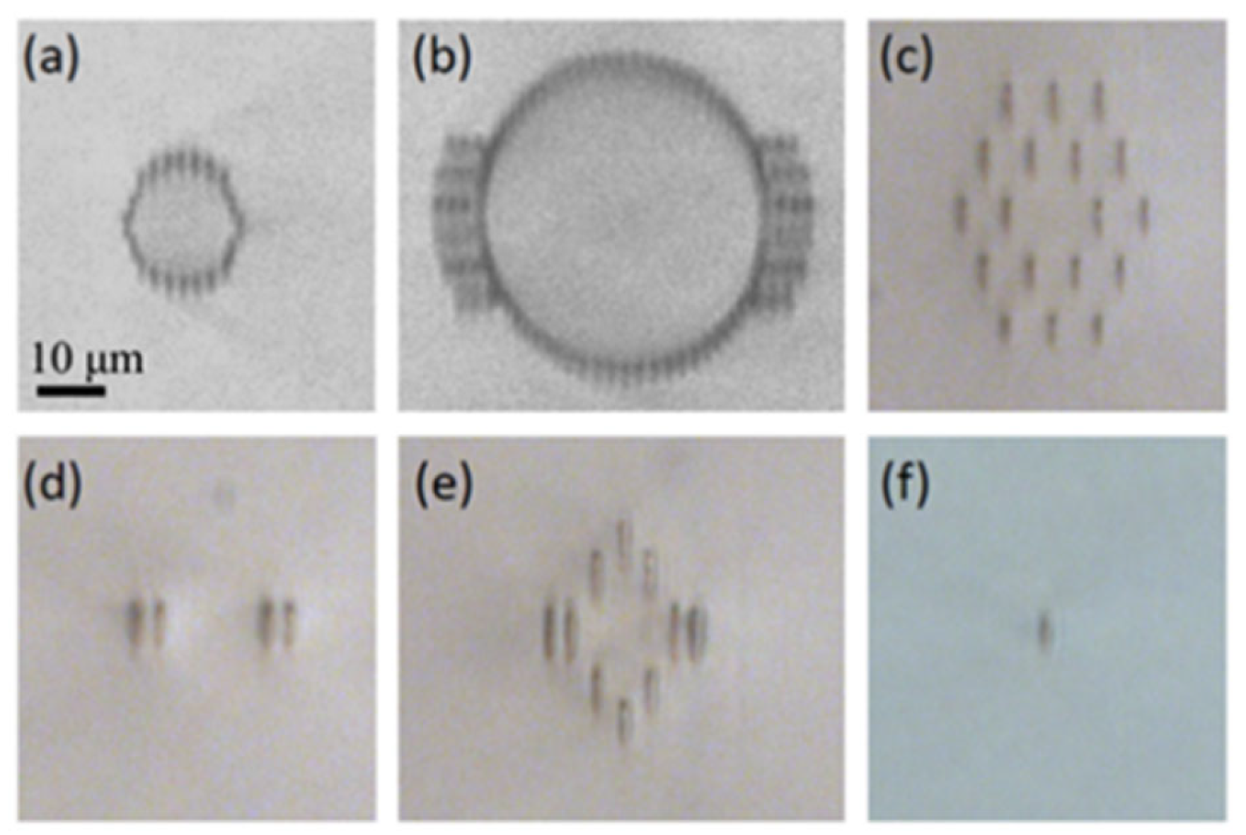
2. Femtosecond Laser Direct–Writing Technology in Optical Waveguide

The common methods for fabricating optical waveguides include ion exchange [4], ion implantation [8], vapor deposition technology [9], FLDW technology [10] and others.
Ion exchange technology is one of the earliest techniques used for optical waveguide fabrication. In 1972, Izawa et al. [11] first used this technology to fabricate optical waveguides on glass substrates. Since then, this technology has been rapidly developed, matured and widely applied in the fabrication of glass waveguides. The principle of the ion exchange technology is to exchange source ions (include solid metal sources and molten salt sources) with the cations of network modifiers in the glass. This ion exchange alters the refractive index of the exchange region, thereby forming an optical waveguide structure, typically assisted by thermal (Figure 1a) or electrical (Figure 1b) driving. As shown in Figure 1a, in a certain high–temperature environment, the source ions in the molten salt have free mobility, and due to non–zero migration rates and concentration gradients, they diffuse toward the interior of the glass. Similarly, the ions of the network modifiers in the glass substrate diffuse outward because of non–zero mobility, differences in ion concentration, and weaker bond energy, completing the exchange with source ions [4]. The free diffusion mechanism of this thermal ionic exchange results in the fabrication of a surface waveguide with a gradient refractive index distribution. In order to better control the refractive index distribution of the waveguide, an external electric field is typically applied to the glass substrate, initiating the potential energy difference mechanism for ion exchange, as shown in Figure 1b. Under the influence of an external electric field, the source ions enter the glass matrix in a directed manner, and the ion diffuses from the exchange surface into the interior of the glass [12]. Ion exchange technology makes it possible to mass–produce high–quality waveguides, but the controllability of the thickness and refractive index distribution of the optical waveguides is still insufficient. Furthermore, this technology is only applicable to waveguide fabrication in glass and a few crystal materials (such as LiNbO3), which restricts its application in the field of waveguide lasers.
The principle of ion implantation technology is that specific ions, accelerated by an ion accelerator, interact with the lattice of the target crystal after entering it. This interaction disrupts the crystal structure and creates localized lattice distortions or defects. As a result, the lattice stress field or bulk density in the specific region changes, ultimately leading to a modification in the refractive index of that region and forming an optical waveguide structure [13]. Compared to ion exchange technology, waveguides fabricated by ion implantation technology show better surface uniformity due to the precise control over the number of implanted ions and the implantation depth. And because the ion implantation process is a non–equilibrium process, it is not limited by factors such as the solid solubility of the implanted atoms in the target substrate or the diffusion coefficient. Theoretically, any element can be implanted into any substrate material. However, the fabrication process requires a high vacuum environment and is complex in terms of the production technique.
FLDW is a micro–nano fabrication technology that utilizes the nonlinear interaction between the laser beam, which is focused on the surface or inside of a material through the lens, and the material at the focus, leading to changes in the material properties [14]. Therefore, FLDW technology can achieve internal three–dimensional fabricating. In the process of fabricating optical waveguides, the focused femtosecond laser exhibits ultra–high peak power density. As a result, nonlinear processes such as multiphoton absorption, tunneling ionization, and avalanche ionization occur in the focal region of the material, leading to the accumulation of a large number of free electrons that form the plasma [15]. Plasma will continue to absorb energy from the pulse laser, and this process will diminish as the plasma frequency approaches the laser frequency [16]. Currently, the exact mechanisms and dynamics of how plasma transfers energy to the lattice remain unknown. Due to the pulse duration of the femtosecond laser being much shorter than the time required for crystal melting, the energy of the laser is not transferred to the lattice before the irradiation ends [17]. This significantly reduces the thermal damage caused during processing. In terms of the fabrication of optical waveguides, the FLDW technology has the advantages of higher processing precision, greater flexibility, and the capability of three–dimensional processing.
By controlling the focusing area and scanning path of the femtosecond laser, complex optical waveguide structures can be directly fabricated inside the material. In the actual fabrication of optical waveguides, there are typically two methods to achieve relative displacement between the laser focus and the sample [18]. One method, as shown in Figure 2a, involves fixing the sample and then changing the position and angle of the beam in front of the objective lens using two electrically controlled mirrors. When the beam position shifts significantly, the focusing objective lens needs to be moved accordingly. The system cost of this scanning method is relatively low, but the processing scope is often limited. Another method, as shown in Figure 2b, involves fixing the laser focal region and placing the sample on a three–dimensional movable processing stage. The optical waveguide is fabricated by moving the stage. A motion displacement platform with suitable precision and travel range can achieve high–precision and wide–range fabrication of optical waveguides. There are two methods to fabricate a waveguide trace: one is the longitudinal scanning method, as shown in Figure 2c, which means the sample moves in the direction of the laser incidence. The optical waveguides fabricated using this method have a circular cross–sectional morphology. However, due to limitations, such as the working distance of the objective lens, it is often challenging to fabricate a waveguide with arbitrary sizes and structures. The other is the transverse scanning method, as shown in Figure 2d, which means the sample movement direction is perpendicular to the direction of the incident laser. In the transverse scanning method, the embedding depth, overall dimensions, and spatial structure of the waveguide are no longer restricted by the working distance of the focusing elements, allowing for greater design flexibility. When using the transverse scanning method, the non–uniform energy distribution of the laser at the focal point caused by the aberrations of the focusing objective lens results in the waveguide cross–section not being a uniform circle. However, by employing beam shaping techniques to assist the femtosecond laser processing, the waveguide morphology and fundamental properties can be well–controlled. When fabricating optical waveguides with the femtosecond laser, there are usually two types of material modifications [19]: Type–I modification (increase in refractive index in the laser focal region) and Type–II modification (decrease in refractive index in the laser focal region). The parameters of femtosecond laser processing (such as pulse duration, pulse energy, and repetition rate) and the inherent properties of the material (such as band gap, hardness, and refractive index) will affect the type of material modification that occurs at the laser focus. In general, when the single pulse energy of the femtosecond laser is relatively low, it is easier to induce Type–I modification in the material; as the single pulse energy increases, the damage to the material from the femtosecond laser gradually intensifies, eventually leading to the appearance of Type–II modification [20]. Currently, Type–I modifications are more commonly in amorphous glasses, and only appear in a few crystalline materials such as LiNbO3 [21] and polycrystalline ZnSe [22]. In contrast, Type–II modifications can be realized in both glasses and anisotropic nonlinear optical crystal materials.
The refractive index of the material increases in the Type–I modified region, so the entire femtosecond laser–scanned area directly forms the waveguide region, offering greater flexibility during fabrication. However, in the region where the waveguide is formed, the fluorescence characteristics and laser characteristics of the crystal itself cannot be retained. In addition, optical waveguides based on Type–I modification generally have low thermal stability. When the waveguide is in a high–temperature state, the refractive index change in the scanned area will even disappear, which also limits the applications in the high–temperature environment and the high–power setting. The refractive index of the materials in Type–II modified regions is reduced, and the area enveloped by the scanned area is the waveguide region. Therefore, Type–II modified waveguides better retain the properties of the material itself. Compared to Type–I optical waveguides, Type–II optical waveguides have better thermal stability. Type–II optical waveguides can be divided into dual–line optical waveguides [23], cladding optical waveguides [24], and photonic crystal–like optical waveguides [25] according to the different scanning trajectory structures. Dual–line straight waveguides [26] and cladding straight waveguides [27] are most commonly used to achieve waveguide lasers. In addition, some new waveguide structures are also used to realize the output of the waveguide laser, such as Y–branch waveguides [28,29], S–curved waveguides [25], multi–cladding waveguide structure waveguides [10,30], spiral optical waveguides [31], and optical–lattice–like structure waveguides [32].
The main factors affecting the performance of optical waveguides by FLDW technology include the output parameters of the laser, the focusing method, and the precision of the translation stage. Commonly used types of femtosecond laser sources for directly writing optical waveguides include solid–state Ti:sapphire lasers [33], fiber lasers [34], and optical parametric oscillators. The pulse duration of the direct–writing light source, single–pulse energy, and pulse repetition rate will affect the size of the affected area and the roughness of its edges. As mentioned above, multiphoton nonlinear absorption is a common process in the fabrication of optical waveguides by FLDW technology. The shorter the center wavelength of the direct–writing light source, the higher the energy of the single photons it emits, and the more efficiently the material absorbs energy. In addition, laser sources with shorter center wavelengths have a smaller diffraction–limited spot size after focusing, allowing for more precise writing of waveguides. The center wavelength of direct–writing light sources is typically 1 μm, 800 nm or 500 nm. The impact of the focusing method on the engraving effect mainly lies in the size of the focused spot. The smaller the diameter of the focused light spot, the finer the structure engraved. Using an objective lens with a larger numerical aperture (NA), such as an oil immersion objective, or using an aspherical lens with smaller aberrations, helps to realize the smaller focused spot. The structure combining a focusing objective lens with beam shaping can enhance beam quality, optimize the focused spot shape, and improve processing precision [35]. Scanning speed affects the quality and uniformity of the optical waveguide. If the scanning speed is too fast, it may lead to uneven processing, while if it is too slow, it might cause excessive damage to the material. The edges of the optical waveguide can be smoothed by using multiple laser–scanning methods. The design of the waveguide path affects its propagation characteristics and overall performance. It is necessary to consider the shape, size, and layout of the waveguide. The optimization of these factors can achieve high–quality FLDW of optical waveguides.

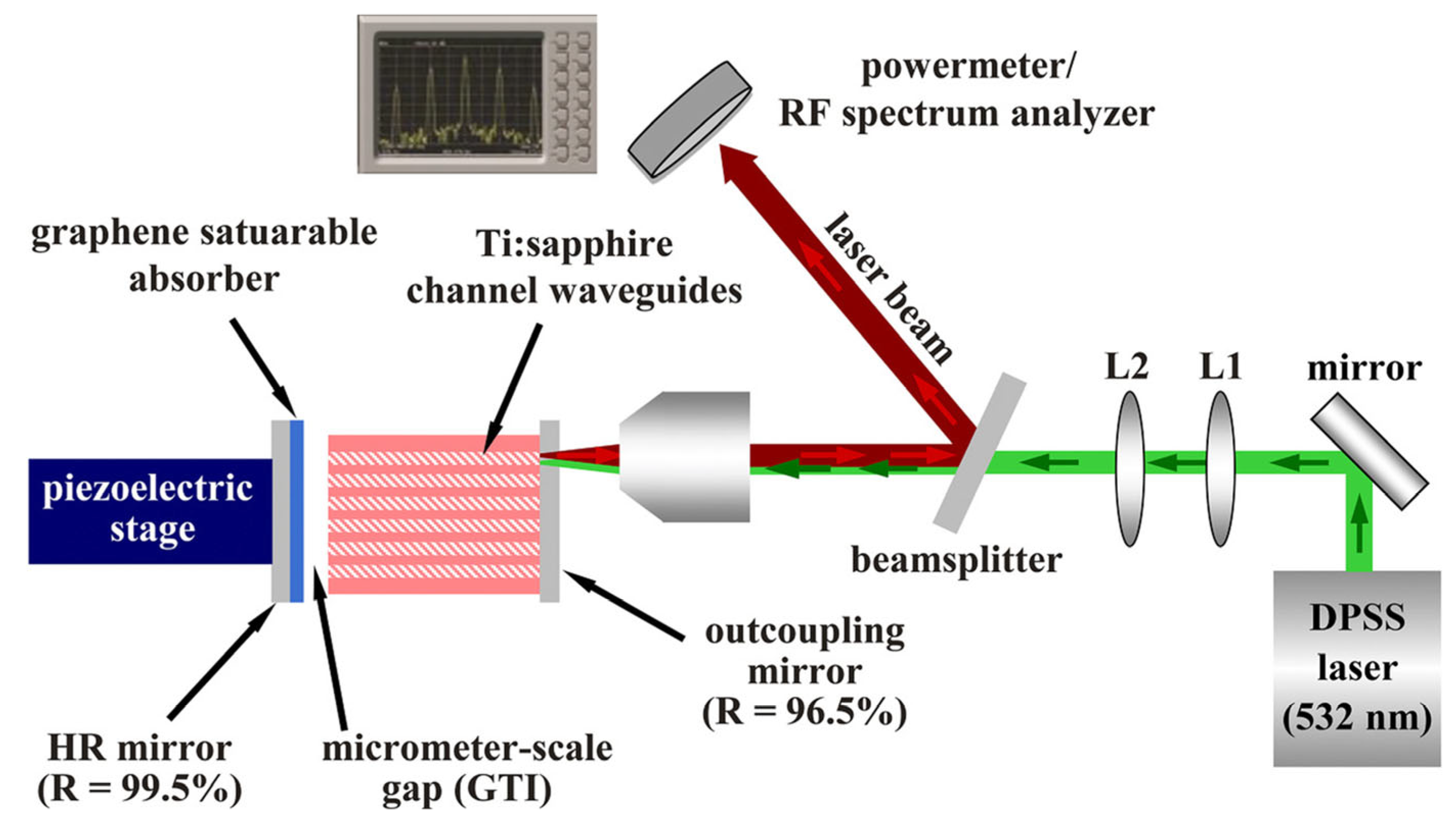
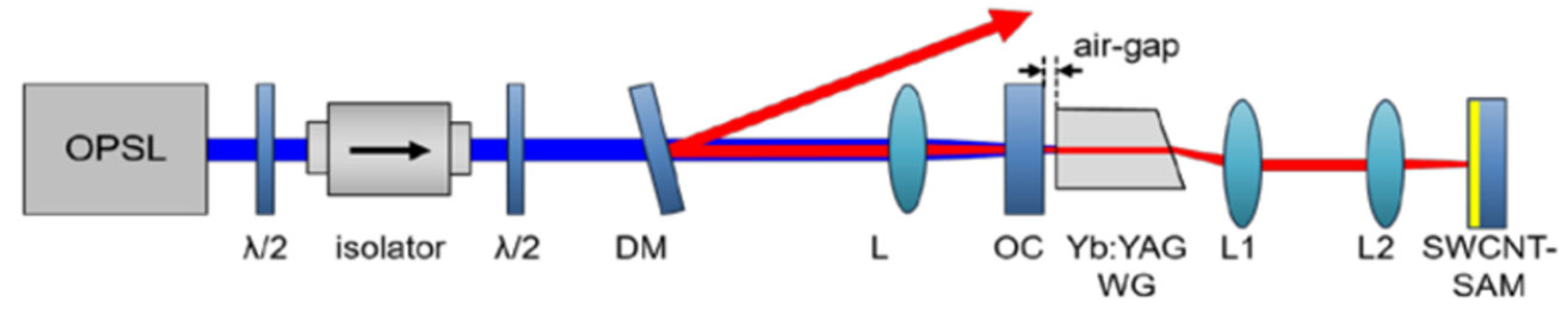
3. Development of Femtosecond Laser Direct–Writing Optical Waveguide Laser

As early as 2004, Taccheo et al. [36] first achieved the output of a CW waveguide laser on Er–Yb co–doped phosphate glass. The Type–I waveguide was fabricated using the processing laser with a center wavelength of 520 nm, a pulse duration of 300 fs, a repetition rate of 166 kHz, and a single–pulse energy of 270 nJ. The writing process employed a 100× oil–immersion microscope objective (NA = 1.4), with a writing speed of 500 μm/s. Since then, various CW waveguide lasers have been realized in different gain media. Table 1 summarizes the work of some waveguide lasers with a CW laser output.
In Table 1, the output laser wavebands involve visible to mid–infrared wavebands. In the visible waveband, the most commonly used crystals are doped with praseodymium (Pr3⁺), such as Pr:SrAl12O19 and Pr:LLF crystals. Pr3+ shows a strong absorption peak at approximately 445 nm, and its emission spectrum covers the entire visible range from 480 nm to 720 nm. In 2023, Baiocco et al. [58] used an amplified femtosecond laser system (800 nm, 60 fs, 5 kHz, with a 40× microscope objective with an NA of 0.65) to fabricate various types of waveguides in Pr:LLF crystals with FLDW technology. These include Type–I waveguides, dual–line waveguides, and suppressing cladding structures. Some of the waveguide end–face images are shown in Figure 3. Transmission measurements were conducted on all waveguides, and the lowest transmission loss of 0.12 dB/cm was obtained with a circular ear–like cladding of a 18 μm radius. They realized CW laser outputs at 604 nm, 645 nm, 721 nm, and 698 nm utilizing different waveguides. In 2024, they [35] further improved the performance of waveguide lasers. By using diode–pumped Pr:LiLuF4 waveguide lasers, they achieved laser emission at 604 nm with a maximum output power of 275 mW (three times than what they had done in 2023) and a slope efficiency of 40%. They also achieved laser emission at 721 nm with an output power of 310 mW (4.4 times than what they had done in 2023) and a slope efficiency of 50%. In addition, they achieved a laser emission at 523 nm in a diode–pumped waveguide, with a maximum output power of 65 mW and a slope efficiency of 11%. In the same year, they tested the thermal stress stability of high–efficiency diode–pumped waveguide lasers based on Pr:LiLuF4. In a 70 °C environment, the maximum output power of the 604 nm and 721 nm lasers remains unchanged, and the corresponding slope efficiency does not vary, which confirms the high–temperature stability of the laser [59].
Compared to milliwatt–level laser outputs in other bands, watt–level outputs can be achieved in the 1 μm waveband. The output power of CW waveguide lasers can reach up to approximately 5.7 W, with a slope efficiency of 78% [41]. Near–infrared waveguide lasers have now achieved continuous–wave mode–locked (CWML) output.
Lasers with wavelengths above 2 μm, especially mid–infrared lasers, are safe for the human eye, have high penetration, and overlap with the absorption peak of biological molecules. This makes them highly promising applications in remote sensing, wind measurement, coherent light detection, and biomedical fields. In 2024, Ayevi et al. [57] inscribed cladding waveguides with a diameter of 70 µm in Er:YLiF4 crystals. The laser used for inscription had a center wavelength of 800 nm, a repetition rate of 1 kHz, a pulse duration of 120 fs, and a single–pulse energy of 1 μJ. The inscription process employed a 40× objective lens with a NA of 0.65. The transmission loss of the final etched optical waveguide is 0.41 dB/cm at 780 nm, with a refractive index contrast of 7.1 × 10⁻⁴. A CW laser output with a power of up to 66 mW was achieved at 2808 nm, corresponding to a slope efficiency of 19.6%.
The typical laser cavity structure of CW waveguide lasers is shown in Figure 4a. Usually, a planar dichroic input mirror and an output coupling (OC) mirror are added on both sides of the optical waveguide. This spatial structure will compromise the ultra–compact advantages of waveguide lasers and hinder monolithic integration. To achieve highly integrated waveguide lasers, researchers have considered coating technology [60] and mirrorless structures [30,48]. In 2019, Tan et al. fabricated a dual–line waveguide in a Nd:GdVO4 crystal using a processing laser with a center wavelength of 1047 nm, a repetition rate of 200 kHz, a pulse duration of 350 fs, and a single–pulse energy of 700 nJ, achieving a low transmission loss of 0.5 dB/cm. They achieved high conversion efficiency CW laser output at 1064 nm wavelength using this waveguide, employing a mirrorless structure. Each end face of the waveguide had a reflectivity of 10% due to Fresnel reflection. At a pump power of 569 mW, the waveguide laser achieved the maximum output power of 256 mW, with a slope efficiency of 70%. These results approach the quantum defect limit of 76% between pump photons and laser photons [48].
In addition to achieving CW output with narrow linewidth, waveguide lasers can also achieve pulse laser outputs with an ultra–high repetition rate. Waveguide lasers use a semiconductor saturable absorber mirror (SESAM) and low–dimensional nanomaterials as a saturable absorber (SA) to achieve pulse laser outputs. Currently, SESAM is the most viable option due to its high damage threshold and excellent stability. However, it has the disadvantage of narrow working wavelength and high cost. Compared with SESAM, low–dimensional materials, especially two–dimensional SA materials (graphene [61], single–walled carbon nanotubes (SWCNTs) [33] and transition metal sulfides [62], etc.) have been more widely used in waveguide lasers to achieve pulse laser output due to their wide operating wavelength range, short bleaching time and low cost. There are two common deposition methods for SA. One is the indirect method shown in Figure 5a. The output of the pulse laser is realized by the coupling of the evanescent field with the SA, and the SA is usually deposited on the surface of the optical waveguide. The other is the direct method shown in Figure 5b. The SA is usually deposited on the surface of the pump mirror. The development of waveguide pulse lasers is shown in Table 2.
As shown in Table 2, the repetition rate of the Q–switched pulse laser is in the order of MHz, and the pulse duration is in the order of ns. Currently, there are no Q–switched pulse waveguide laser outputs in the visible wavebands fabricated by FLDW technology. The Q–switched pulse outputs are primarily in the near–infrared range, particularly around the 1 μm waveband, with relatively high slope efficiency. Hakobyan et al. [41] fabricated a low loss (0.5 dB/cm) dual–line waveguide in Yb:YAG crystal using FLDW technology. A SESAM was used as the SA to achieve a Q–switched laser pulse output with a maximum repetition rate of 5.4 MHz, a shortest pulse duration of 11 ns, a maximum pulse energy of 1 μJ, and a slope efficiency of 78%. Recently, in 2023, Liu et al. [62] used a radial polarization vortex femtosecond laser (1030 nm, 220 fs, 1 MHz) to fabricate a cladding waveguide with a transmission loss of 0.85 dB/cm in Yb:CaF2 crystal. By using this waveguide and ReS0.8Se1.2 as the SA, a Q–switched pulse laser output was achieved around 1045.2 nm. The output Q–switched pulses have an adjustable repetition rate ranging from 125 kHz to 692.5 kHz, with the shortest pulse duration of 513 ns. In the same year, Xiong et al. [56] fabricated a cladding waveguide in Tm:YLF crystal, utilizing Bi2Se3 as an SA. A Q–switched pulse laser output was achieved near 1877 nm, with a repetition rate of 421.6 kHz and a pulse duration of 392.8 ns, achieving the maximum output laser power of 474 mW. In the mid–infrared waveband, in 2024, Ayevi et al. [57] achieved a self–mode–locked Q–switched pulse output at around 2717 nm using a cladding waveguide with a diameter of 70 µm written into an Er:YLiF4 crystal. The pulse was generated with a pulse duration of 240 ns, with an average power of 51 mW, a repetition rate of 368 kHz, and a slope efficiency of 15.2%.
The repetition rate of a mode–locked waveguide laser can reach GHz, and the pulse duration can reach femtoseconds. Currently, mode–locked waveguide lasers have not appeared in the visible and mid–infrared wavebands. The biggest challenge is the balance of intracavity dispersion. The shortest pulse duration output from the mode–locked waveguide laser is 180 fs, which was achieved in 2018 by Grivas et al. [26] using a dual–line waveguide (with a spacing of 24 μm) inside Ti:sapphire crystals. The waveguide was fabricated using a mode–locked regenerative amplifier Yb:KGW laser (1030 nm, 180 fs, 1 kHz, 1.5 μJ). The experimental setup is shown in Figure 6. The mode–locking laser cavity commonly consists of two high–reflective (HR) mirrors: one end has a thin reflective mirror at the front face of the waveguide (with a reflectance of 96.5% for the signal light), which also serves the functions of coupling the pump light and the output signal light. The HR mirror (RB = 99.5%) on the other end is coated with a graphene layer that can act as an SA and is mounted on a piezoelectric stage close to the end face of the waveguide. The air gap between the end face of the waveguide and the SA mirror can produce a Gires–Tournois interferometer (GTI) effect to compensate for dispersion within the cavity. Ultimately, they achieved a CWML laser output with a repetition rate of 21.25 GHz and a pulse duration of 41.4 fs at 798.5 nm.
Choi et al. [40] used a femtosecond laser to write a cladding waveguide in Yb:YAG crystal in 2018 and realized a Yb3+–doped CWML waveguide laser based on single–walled carbon nanotubes as SA for the first time. The experimental setup is shown in Figure 7. The OC mirror with a reflection of 5% at laser wavelength is positioned at the entrance of the waveguide. It features a GTI coating that provides a total group delay dispersion of −1300 fs2 to compensate for dispersion. In the experiment, the piezoelectric control stage can be used to adjust the distance of the thin air gap between the OC mirror and the waveguide surface to control the dispersion in the laser cavity. Finally, the CWML pulse output with a center wavelength of 1040 nm, a repetition rate of 2.08 GHz, and a pulse duration of 1.89 ps is realized. The mode–locking pump power threshold is 1.8 W, the maximum CWML output power is 322 mW, and the slope efficiency is 11.3%.
In addition to the GTI effect, another method for compensating dispersion is to introduce optical components with specific dispersion characteristics.
Similar to CW waveguide lasers, most pulse waveguide lasers use a spatially optical path structure, which is not conducive to integration. Mirrorless waveguide lasers are one of the most straightforward solutions towards achieving photonics integration [66]. In addition, more diverse structures also need to be explored to achieve better performance of pulse laser output in optical waveguides.

4. Conclusions

This paper mainly introduces the research progress of femtosecond laser direct waveguide lasers. In Section 2, we introduce the application of FLDW technology in optical waveguide fabrication. Firstly, the principle of FLDW technology is explained. Secondly, we summarize the common scanning methods: the sample fixed–laser focus moving method and the laser focus fixed–sample moving method. Thirdly, we generalize the basic and some special types of optical waveguides. Finally, we analyze the factors that affect the performance of optical waveguides. At present, FLDW technology has irreplaceable advantages in the flexible fabrication of three–dimensional internal channel waveguides. However, the lattice distortion and defects in the laser–damaged region during the fabrication process will cause scattering loss, which makes it challenging to fabricate ultra–low loss optical waveguides (<0.5 dB/cm). In order to reduce the transmission loss of the optical waveguide, researchers have proposed to optimize the light source, such as using the spiral phase plate to convert the Gaussian femtosecond laser into a vortex laser and using the light field control technology to shape the Gaussian beam of the femtosecond laser.
In Section 3, we summarize the development of CW and pulse waveguide lasers. The materials used to realize the output of the CW waveguide laser in the visible waveband are mainly Pr3+–doped materials. Some frequency–doubling crystals can also realize the output of the CW waveguide laser in the visible waveband. The near–infrared CW waveguide laser has the most achievements compared to other wavebands and the CW laser at 1 μm can achieve an average power output in the order of watts, mainly concentrated in Yb3+– and Nd3+–doped crystals and phosphate glass. The maximum output wavelength of the mid–infrared band realized by the CW waveguide laser is 2808 nm. In the optical waveguide laser, the most common method to achieve pulse output is to add an SA in the laser cavity. The most common SAs are two–dimensional nanomaterials, such as graphene and SWCNTs. The repetition rate of Q–switched pulse lasers output by waveguide lasers is typically in the order of MHz, and the pulse duration is in the order of ns. At present, the Q–switched pulse laser output in the mid–infrared waveband has been realized, but that in the visible waveband is still absent. The average output power of the Q–switched pulse at the 1 μm band is up to the watt level. Mode–locked pulse lasers can achieve a repetition rate up to the GHz level, and this has only been reported in the near–infrared waveband.
The primary challenge of mode–locked pulse output lies in balancing the dispersion within the cavity. The most common method to achieve dispersion balance has two kinds: one is to utilize the GTI effect between the cavity mirror and the air gap at the waveguide end face, but this method is prone to instability; the other is to increase the dispersion compensation element in the cavity by using the extended cavity [67], but this will increase the cavity length. Due to the characteristics of FLDW technology, it is possible to write chirped gratings in the cavity to balance dispersion [65]. Moreover, employing the original Fresnel reflection at the waveguide end face instead of using a cavity mirror to achieve an ultra–compact waveguide structure is a straightforward and efficient method to address the limitations of the current waveguide laser integration with a spatial structure.

Author Contributions

Writing—original draft preparation, B.Y. and Y.Z.; writing—review and editing Z.Z. and X.D.; supervision, J.W. All authors have read and agreed to the published version of the manuscript.

Funding

This research was funded by the National Natural Science Foundation of China, grant number 62275209.

Data Availability Statement

No new data were created or analyzed in this study. Data sharing is not applicable to this article.

Conflicts of Interest

The authors declare no conflicts of interest.

References

  1. Bae, J.E.; Loiko, P.; Normani, S.; Brasse, G.; Benayad, A.; Braud, A.; Camy, P. Er:LiYF4 planar waveguide laser at 2.8 μm. Appl. Phys. Lett. 2024, 125, 081101. [Google Scholar] [CrossRef]
  2. Waeselmann, S.H.; Rüter, C.E.; Kip, D.; Kränkel, C.; Huber, G. Nd:sapphire channel waveguide laser. Opt. Mater. Express 2017, 7, 2361–2367. [Google Scholar] [CrossRef]
  3. Kurilchik, S.V.; Prentice, J.J.; Eason, R.W.; Mackenzie, J.I. Characterisation and laser performance of a Yb:LuAG double–clad planar waveguide grown by pulse laser deposition. Appl. Phys. B 2019, 125, 201. [Google Scholar] [CrossRef]
  4. Hao, Y.; Liu, J.; Che, L.; Wang, S.; Meng, H.; Liu, X. Buried Optical Waveguide in Photo–Thermo–Refractive Glass by Ion Exchange Technology. IEEE Photonics Technol. Lett. 2023, 35, 793–796. [Google Scholar] [CrossRef]
  5. Xiang, B.; Ren, X.; Ruan, S.; Wang, L.; Yan, P.; Han, H.; Wang, M.; Yin, J. Visible to near–infrared supercontinuum generation in yttrium orthosilicate bulk crystal and ion implanted planar waveguide. Sci. Rep. 2016, 6, 31612. [Google Scholar] [CrossRef]
  6. Jia, Y.C.; Wang, S.X.; Chen, F. Femtosecond laser direct writing of flexibly configured waveguide geometries in optical crystals: Fabrication and application. Opto–Electron. Adv. 2020, 3, 190042. [Google Scholar] [CrossRef]
  7. Davis, K.M.; Miura, K.; Sugimoto, N.; Hirao, K. Writing waveguides in glass with a femtosecond laser. Opt. Lett. 1996, 21, 1729–1731. [Google Scholar] [CrossRef]
  8. Hu, H.; Lu, F.; Chen, F.; Shi, B.-R.; Wang, K.-M.; Shen, D.-Y. Monomode optical waveguide in lithium niobate formed by MeV Si+ ion implantation. J. Appl. Phys. 2001, 89, 5224–5226. [Google Scholar] [CrossRef]
  9. Yevnin, M.; Atar, G.; Čampelj, S.; Lenardič, B.; Kaplan, N.; Sherman, V.; Gvishi, R.; Sfez, B.; Eger, D. Low–Loss Waveguides by Planar Modified Chemical Vapor Deposition. J. Light. Technol. 2020, 38, 792–796. [Google Scholar] [CrossRef]
  10. Wu, P.; He, S.; Liu, H. Annular waveguide lasers at 1064 nm in Nd:YAG crystal produced by femtosecond laser inscription. Appl. Opt. 2018, 57, 5420–5424. [Google Scholar] [CrossRef]
  11. Izawa, T.; Nakagome, H. Optical waveguide formed by electrically induced migration of ions in glass plates. Appl. Phys. Lett. 1972, 21, 584–586. [Google Scholar] [CrossRef]
  12. Alzahrani, A.S.; Pintori, G.; Sglavo, V.M. Conventional and electric field–assisted ion exchange on glass–ceramics for dental applications. J. Eur. Ceram. Soc. 2021, 41, 5341–5348. [Google Scholar] [CrossRef]
  13. Gibbons, J.F. Ion implantation in semiconductors–Part I: Range distribution theory and experiments. Proc. IEEE 1968, 56, 295–319. [Google Scholar] [CrossRef]
  14. He, F.; Liao, Y.; Lin, J.; Song, J.; Qiao, L.; Cheng, Y.; Sugioka, K. Femtosecond Laser Fabrication of Monolithically Integrated Microfluidic Sensors in Glass. Sensors 2014, 14, 19402–19440. [Google Scholar] [CrossRef]
  15. Sugioka, K.; Xu, J.; Wu, D.; Hanada, Y.; Wang, Z.; Cheng, Y.; Midorikawa, K. Femtosecond laser 3D micromachining: A powerful tool for the fabrication of microfluidic, optofluidic, and electrofluidic devices based on glass. Lab. A Chip. 2014, 14, 3447–3458. [Google Scholar] [CrossRef]
  16. Rethfeld, B.; Sokolowski-Tinten, K.; von der Linde, D.; Anisimov, S.I. Timescales in the response of materials to femtosecond laser excitation. Appl. Phys. A 2004, 79, 767–769. [Google Scholar] [CrossRef]
  17. Ams, M.; Marshall, G.D.; Dekker, P.; Dubov, M.; Mezentsev, V.K.; Bennion, I.; Withford, M.J. Investigation of Ultrafast Laser–Photonic Material Interactions: Challenges for Directly Written Glass Photonics. IEEE J. Sel. Top. Quantum Electron. 2008, 14, 1370–1381. [Google Scholar] [CrossRef]
  18. Correa, D.S.; Almeida, J.M.P.; Almeida, G.F.B.; Cardoso, M.R.; De Boni, L.; Mendonça, C.R. Ultrafast Laser Pulses for Structuring Materials at Micro/Nano Scale: From Waveguides to Superhydrophobic Surfaces. Photonics 2017, 4, 8. [Google Scholar] [CrossRef]
  19. Gross, S.; Dubov, M.; Withford, M.J. On the use of the Type I and II scheme for classifying ultrafast laser direct–write photonics. Opt. Express 2015, 23, 7767–7770. [Google Scholar] [CrossRef]
  20. Shen, Y.; Jia, Y.; Chen, F. Femtosecond laser–induced optical waveguides in crystalline garnets: Fabrication and application. Opt. Laser Technol. 2023, 164, 109528. [Google Scholar] [CrossRef]
  21. Thomson, R.R.; Campbell, S.; Blewett, I.J.; Kar, A.K.; Reid, D.T. Optical waveguide fabrication in z–cut lithium niobate (LiNbO3) using femtosecond pulses in the low repetition rate regime. Appl. Phys. Lett. 2006, 88, 111109. [Google Scholar] [CrossRef]
  22. Macdonald, J.R.; Thomson, R.R.; Beecher, S.J.; Psaila, N.D.; Bookey, H.T.; Kar, A.K. Ultrafast laser inscription of near–infrared waveguides in polycrystalline ZnSe. Opt. Lett. 2010, 35, 4036–4038. [Google Scholar] [CrossRef]
  23. Reichert, F.; Calmano, T.; Müller, S.; Marzahl, D.T.; Metz, P.W.; Huber, G. Efficient visible laser operation of Pr,Mg:SrAl12O19 channel waveguides. Opt. Lett. 2013, 38, 2698–2701. [Google Scholar] [CrossRef]
  24. Ren, Y.; Chen, F.; Vázquez de Aldana, J.R. Near–infrared lasers and self–frequency–doubling in Nd:YCOB cladding waveguides. Opt. Express 2013, 21, 11562–11567. [Google Scholar] [CrossRef]
  25. Li, L.; Li, Z.; Nie, W.; Romero, C.; Aldana, J.R.V.d.; Chen, F. Femtosecond–Laser–Written S–Curved Waveguide in Nd:YAP Crystal: Fabrication and Multi–Gigahertz Lasing. J. Light. Technol. 2020, 38, 6845–6852. [Google Scholar] [CrossRef]
  26. Grivas, C.; Ismaeel, R.; Corbari, C.; Huang, C.-C.; Hewak, D.W.; Lagoudakis, P.; Brambilla, G. Generation of Multi–Gigahertz Trains of Phase–Coherent Femtosecond Laser Pulses in Ti:Sapphire Waveguides. Laser Photonics Rev. 2018, 12, 1800167. [Google Scholar] [CrossRef]
  27. Wang, S.; Liu, H.; Mu, W.; Ren, Y.; Jia, Z.; Fu, X.; Sun, X.; Jia, Y. Dual–wavelength self–Q–switched mode–locked waveguide lasers based on Nd:LGGG cladding waveguides. Opt. Mater. Express 2022, 12, 854–862. [Google Scholar] [CrossRef]
  28. Calmano, T.; Kränkel, C.; Huber, G. Laser oscillation in Yb:YAG waveguide beam–splitters with variable splitting ratio. Opt. Lett. 2015, 40, 1753–1756. [Google Scholar] [CrossRef]
  29. Liu, H.; Aldana, J.R.V.d.; Hong, M.; Chen, F. Femtosecond Laser Inscribed Y–Branch Waveguide in Nd:YAG Crystal: Fabrication and Continuous–Wave Lasing. IEEE J. Sel. Top. Quantum Electron. 2016, 22, 227–230. [Google Scholar] [CrossRef]
  30. Jia, Y.; He, R.; Vázquez de Aldana, J.R.; Liu, H.; Chen, F. Femtosecond laser direct writing of few–mode depressed–cladding waveguide lasers. Opt. Express 2019, 27, 30941–30951. [Google Scholar] [CrossRef]
  31. Peng, Y.-P.; Zou, X.; Bai, Z.; Leng, Y.; Jiang, B.; Jiang, X.; Zhang, L. Mid–infrared laser emission from Cr:ZnS channel waveguide fabricated by femtosecond laser helical writing. Sci. Rep. 2015, 5, 18365. [Google Scholar] [CrossRef] [PubMed]
  32. Jia, Y.; Cheng, C.; Vázquez de Aldana, J.R.; Castillo, G.R.; Rabes, B.d.R.; Tan, Y.; Jaque, D.; Chen, F. Monolithic crystalline cladding microstructures for efficient light guiding and beam manipulation in passive and active regimes. Sci. Rep. 2014, 4, 5988. [Google Scholar] [CrossRef]
  33. Bae, J.E.; Park, T.G.; Kifle, E.; Mateos, X.; Aguiló, M.; Díaz, F.; Romero, C.; Rodríguez Vázquez de Aldana, J.; Lee, H.; Rotermund, F. Carbon nanotube Q–switched Yb:KLuW surface channel waveguide lasers. Opt. Lett. 2020, 45, 216–219. [Google Scholar] [CrossRef]
  34. Li, S.-L.; Ye, Y.-K.; Wang, H.-L. Cladding waveguide lasers in femtosecond laser written Nd:KGW waveguides. Opt. Mater. 2020, 110, 110517. [Google Scholar] [CrossRef]
  35. Chen, D.; Chen, Z.; Yang, Y.; Wang, Y.; Han, X.; Lau, K.Y.; Wu, Z.; Zou, C.; Zhang, Y.; Xu, B.; et al. 3D Laser Writing of Low–Loss Cross–Section–Variable Type–I Optical Waveguide Passive/Active Integrated Devices in Single Crystals. Adv. Mater. 2024, 36, 2404493. [Google Scholar] [CrossRef] [PubMed]
  36. Taccheo, S.; Della Valle, G.; Osellame, R.; Cerullo, G.; Chiodo, N.; Laporta, P.; Svelto, O.; Killi, A.; Morgner, U.; Lederer, M.; et al. Er:Yb–doped waveguide laser fabricated by femtosecond laser pulses. Opt. Lett. 2004, 29, 2626–2628. [Google Scholar] [CrossRef]
  37. Baiocco, D.; Lopez-Quintas, I.; Vázquez de Aldana, J.R.; Tonelli, M.; Tredicucci, A. High efficiency diode–pumped Pr:LiLuF4 visible lasers in femtosecond–laser–written waveguides. Opt. Express 2024, 32, 9767–9776. [Google Scholar] [CrossRef]
  38. Calmano, T.; Siebenmorgen, J.; Reichert, F.; Fechner, M.; Paschke, A.-G.; Hansen, N.-O.; Petermann, K.; Huber, G. Crystalline Pr:SrAl12O19 waveguide laser in the visible spectral region. Opt. Lett. 2011, 36, 4620–4622. [Google Scholar] [CrossRef]
  39. Grivas, C.; Corbari, C.; Brambilla, G.; Lagoudakis, P.G. Tunable, continuous–wave Ti:sapphire channel waveguide lasers written by femtosecond and picosecond laser pulses. Opt. Lett. 2012, 37, 4630–4632. [Google Scholar] [CrossRef]
  40. Choi, S.Y.; Calmano, T.; Rotermund, F.; Kränkel, C. 2–GHz carbon nanotube mode–locked Yb:YAG channel waveguide laser. Opt. Express 2018, 26, 5140–5145. [Google Scholar] [CrossRef]
  41. Hakobyan, S.; Wittwer, V.J.; Hasse, K.; Kränkel, C.; Südmeyer, T.; Calmano, T. Highly efficient Q–switched Yb:YAG channel waveguide laser with 5.6  W of average output power. Opt. Lett. 2016, 41, 4715–4718. [Google Scholar] [CrossRef] [PubMed]
  42. Siebenmorgen, J.; Calmano, T.; Petermann, K.; Huber, G. Highly efficient Yb:YAG channel waveguide laser written with a femtosecond–laser. Opt. Express 2010, 18, 16035–16041. [Google Scholar] [CrossRef]
  43. Jia, Y.; Vázquez de Aldana, J.R.; Chen, F. Efficient waveguide lasers in femtosecond laser inscribed double–cladding waveguides of Yb:YAG ceramics. Opt. Mater. Express 2013, 3, 645–650. [Google Scholar] [CrossRef]
  44. Calmano, T.; Siebenmorgen, J.; Hellmig, O.; Petermann, K.; Huber, G. Nd:YAG waveguide laser with 1.3 W output power, fabricated by direct femtosecond laser writing. Appl. Phys. B 2010, 100, 131–135. [Google Scholar] [CrossRef]
  45. Jia, Y.; Cheng, C.; Aldana, J.R.V.d.; Chen, F. Three–Dimensional Waveguide Splitters Inscribed in Nd:YAG by Femtosecond Laser Writing: Realization and Laser Emission. J. Light. Technol. 2016, 34, 1328–1332. [Google Scholar] [CrossRef]
  46. Zhang, C.; Dong, N.; Yang, J.; Chen, F.; Vázquez de Aldana, J.R.; Lu, Q. Channel waveguide lasers in Nd:GGG crystals fabricated by femtosecond laser inscription. Opt. Express 2011, 19, 12503–12508. [Google Scholar] [CrossRef] [PubMed]
  47. Liu, H.; Jia, Y.; Chen, F.; Vázquez de Aldana, J.R. Continuous wave laser operation in Nd:GGG depressed tubular cladding waveguides produced by inscription of femtosecond laser pulses. Opt. Mater. Express 2013, 3, 278–283. [Google Scholar] [CrossRef]
  48. Tan, Y.; Rodenas, A.; Chen, F.; Thomson, R.R.; Kar, A.K.; Jaque, D.; Lu, Q. 70% slope efficiency from an ultrafast laser–written Nd:GdVO4 channel waveguide laser. Opt. Express 2010, 18, 24994–24999. [Google Scholar] [CrossRef]
  49. Pavel, N.; Salamu, G.; Jipa, F.; Zamfirescu, M. Diode–laser pumping into the emitting level for efficient lasing of depressed cladding waveguides realized in Nd:YVO4 by the direct femtosecond–laser writing technique. Opt. Express 2014, 22, 23057–23065. [Google Scholar] [CrossRef]
  50. Ren, Y.; Dong, N.; Macdonald, J.; Chen, F.; Zhang, H.; Kar, A.K. Continuous wave channel waveguide lasers in Nd:LuVO4 fabricated by direct femtosecond laser writing. Opt. Express 2012, 20, 1969–1974. [Google Scholar] [CrossRef]
  51. Liu, H.; An, Q.; Chen, F.; Vázquez de Aldana, J.R.; del Rosal Rabes, B. Continuous–wave lasing at 1.06μm in femtosecond laser written Nd:KGW waveguides. Opt. Mater. 2014, 37, 93–96. [Google Scholar] [CrossRef]
  52. Okhrimchuk, A.G.; Obraztsov, P.A. 11–GHz waveguide Nd:YAG laser CW mode–locked with single–layer graphene. Sci. Rep. 2015, 5, 11172. [Google Scholar] [CrossRef]
  53. Nie, W.; Cheng, C.; Jia, Y.; Romero, C.; Vázquez de Aldana, J.R.; Chen, F. Dual–wavelength waveguide lasers at 1064 and 1079 nm in Nd:YAP crystal by direct femtosecond laser writing. Opt. Lett. 2015, 40, 2437–2440. [Google Scholar] [CrossRef] [PubMed]
  54. Kifle, E.; Mateos, X.; de Aldana, J.R.V.; Ródenas, A.; Loiko, P.; Choi, S.Y.; Rotermund, F.; Griebner, U.; Petrov, V.; Aguiló, M.; et al. Femtosecond–laser–written Tm:KLu(WO4)2 waveguide lasers. Opt. Lett. 2017, 42, 1169–1172. [Google Scholar] [CrossRef]
  55. Bai, Z.; Chen, Z.; Xiong, Y.; Liu, H.; Gao, S.; Ren, Y.; Zhao, X.; Liu, F.; Jia, Y.; Chen, F. Tm,Ho:YLF waveguide lasers at 2.05 µm. Opt. Lett. 2024, 49, 1977–1980. [Google Scholar] [CrossRef] [PubMed]
  56. Xiong, Y.; Wang, S.; Chen, Z.; Sun, X.; Liu, H.; Jia, Y.; Chen, F. Femtosecond laser direct writing of compact Tm:YLF waveguide lasers. Opt. Laser Technol. 2023, 167, 109786. [Google Scholar] [CrossRef]
  57. Ayevi, B.; Morova, Y.; Tonelli, M.; Sennaroglu, A. Er3+:YLiF4 channeled waveguide laser near 2.7–2.8 μm fabricated by femtosecond laser inscription. Opt. Lett. 2024, 49, 1017–1020. [Google Scholar] [CrossRef] [PubMed]
  58. Baiocco, D.; Lopez-Quintas, I.; Vázquez de Aldana, J.R.; Tonelli, M.; Tredicucci, A. Comparative Performance Analysis of Femtosecond–Laser–Written Diode–Pumped Pr:LiLuF4 Visible Waveguide Lasers. Photonics 2023, 10, 377. [Google Scholar] [CrossRef]
  59. Baiocco, D.; Lopez-Quintas, I.; de Aldana, J.R.V.; Tonelli, M.; Tredicucci, A. Thermal analysis of diode–pumped femtosecond–laser–written Pr:LiLuF4 waveguide lasers. Opt. Laser Technol. 2025, 180, 111499. [Google Scholar] [CrossRef]
  60. Kim, M.H.; Calmano, T.; Choi, S.Y.; Lee, B.J.; Baek, I.H.; Ahn, K.J.; Yeom, D.-I.; Kränkel, C.; Rotermund, F. Monolayer graphene coated Yb:YAG channel waveguides for Q–switched laser operation. Opt. Mater. Express 2016, 6, 2468–2474. [Google Scholar] [CrossRef]
  61. Ponarina, M.V.; Okhrimchuk, A.G.; Rybin, M.G.; Smayev, M.P.; Obraztsova, E.D.; Smirnov, A.V.; Zhluktova, I.V.; Kamynin, V.A.; Dolmatov, T.V.; Bukin, V.V.; et al. Dual–wavelength generation of picosecond pulses with 9.8 GHz repetition rate in Nd:YAG waveguide laser with graphene. Quantum Electron. 2019, 49, 365. [Google Scholar] [CrossRef]
  62. Liu, K.; Dong, Y.; Zhang, Z.; Duan, X.; Guo, R.; Zhai, Z.; Wang, J. MHz repetition rate femtosecond radially polarized vortex laser direct writing Yb:CaF2 waveguide laser operating in continuous–wave and pulse regimes. Nanophotonics 2024, 13, 9–18. [Google Scholar] [CrossRef]
  63. Bae, J.E.; Mateos, X.; Aguiló, M.; Díaz, F.; Vázquez de Aldana, J.R.; Romero, C.; Lee, H.; Rotermund, F. Transition of pulse operation from Q–switching to continuous–wave mode–locking in a Yb:KLuW waveguide laser. Opt. Express 2020, 28, 18027–18034. [Google Scholar] [CrossRef] [PubMed]
  64. Li, Z.; Zhang, Y.; Cheng, C.; Yu, H.; Chen, F. 6.5 GHz Q–switched mode–locked waveguide lasers based on two–dimensional materials as saturable absorbers. Opt. Express 2018, 26, 11321–11330. [Google Scholar] [CrossRef]
  65. Ams, M.; Dekker, P.; Gross, S.; Withford, M.J. Fabricating waveguide Bragg gratings (WBGs) in bulk materials using ultrashort laser pulses. Nanophotonics 2017, 6, 743–763. [Google Scholar] [CrossRef]
  66. Dong, X.; Zhang, B.; Sun, X.; Jia, Y.; Chen, F. 1.8–μm laser operation based on femtosecond–laser direct written Tm:YVO4 cladding waveguides. Opt. Express 2023, 31, 16560–16569. [Google Scholar] [CrossRef]
  67. Jia, Y.; Chen, F. Compact solid–state waveguide lasers operating in the pulse regime: A review [Invited]. Chin. Opt. Lett. 2019, 17, 012302. [Google Scholar]
Figure 1. Ion exchange technology diagram: (a) thermal ion exchange, (b) field-assisted ion exchange.
Photonics 11 00803 g001
Figure 2. The methods to achieve relative displacement between the laser focus and the sample: (a) sample fixed–laser focus moving method [18], (b) laser focus fixed–sample moving method [18]. Waveguide trace writing method: (c) longitudinal scanning method, (d) transverse scanning method.
Photonics 11 00803 g002
Figure 3. Optical microscope pictures of the different waveguide types fabricated in Pr:LLF: (a) circular cladding, (b) ear–like cladding, (c) hexagonal cladding, (d) stress–induced dual–line, (e) stress–induced dual–line with rhombic cladding, (f) single line [58].
Photonics 11 00803 g003
Figure 4. (a) Experimental setup and (b) output pulse characteristics of Nd:GdVO4 crystal CW waveguide laser [48]. WP1 and WP2: waveplate; GTP: Glan Taylor prism; MO: microscope objective lens (20×); CL: convex lens; M1 and M2: laser cavity mirrors adhered to the two end facets of the sample; DB: dichroic beamsplitter; λp and λL: pump and generated laser beam; OC: output coupler.
Photonics 11 00803 g004
Figure 5. The common deposition methods of SA in waveguide lasers: (a) evanescent and (b) direct–field interaction with SA.
Photonics 11 00803 g005
Figure 6. The experimental setup for the Ti:sapphire channel waveguides soliton mode–locking [26]. DPSS laser: diode–pumped solid–state laser. The green arrow represents the propagation direction of the pump light, while the red arrow represents the propagation direction of the signal light.
Photonics 11 00803 g006
Figure 7. The experimental setup of a Yb:YAG crystal CWML waveguide laser from [65]. OPSL: optically pumped semiconductor laser; DM: dichroic beamsplitter; L, L1 and L2: lens; OC: output coupler.
Photonics 11 00803 g007
Table 1. Summary of output parameters of continuous–wave waveguide laser.
Gain mediaWorking Wavelength
(nm)
Cavity ConfigurationLasing Threshold
(mW)
Maximum Output Power
(mW)
Slope Efficiency
(%)
Reference
Pr,Mg:SrAl12O19525.3dual–line108836[23]
Pr:LiLuF4604ear–like cadding27840[37]
Pr:SrAl12O19643.9dual–line19028.18[38]
Ti:sapphire798.5dual–line8414323.5[39]
Yb:YAG1030cadding4341015.2[40]
dual–line5.7 W78[41]
dual–line76575[42]
double–cladding80.262.9[43]
Y–branch dual–line2712.29 W52[28]
Nd:YAG1064Y–branch cladding23122[29]
dual–line631.2959[44]
1 × 4 splitters9021722[45]
Nd:GGG1061dual–line291125[46]
1063cladding27020944.4[47]
Nd:GdVO41063.6dual–line25670[48]
Nd:YVO41064cladding1.528[49]
1065cladding5944357[30]
Nd:LuVO41066.4dual–line983014[50]
Nd:KGW1065dual–line1413352.3[51]
1067cladding140198.539.4[52]
Nd:YAP1064 and 1079cladding243199.833.4[53]
Er–Yb co–doped phosphate glass1533.5Type–I3351.72[36]
Tm:Klu(WO4)21912cladding214615.2[54]
Tm,Ho:YLF2050cladding18147.520.1[55]
Ho:YLF1877cladding107.119[56]
Cr:ZnS2244spiral cladding29.17788.6[31]
Er:YliF42808cladding6619.6[57]
Table 2. A summary of some representative work of waveguide pulse lasers. CWML means continuous–wave mode–locked. QSML is for Q–switched mode–locked. SQSML stands for self–Q–switched mode–locked. SQS means self–Q–switched.
MaterialWorking Wavelength (nm)SACavity ConfigurationOperation
Regime
Repetition RatePulse
Duration
Slope
Efficiency (%)
Reference
Ti:sapphire798.5grapheneDual lineCWML21.25 GHz41.4 fs[26]
Yb:YAG1030SWCNT–SAMDual lineCWML2.08 GHz1.89 ps11.3[40]
SESAMDual lineQ–switched5.4 MHz11 ns74[41]
Yb:KLuW1040SWCNTsSurface claddingQ–switched1.16 MHz88.5 ns61[33]
Yb:KLuW1042.3SWCNTsCladdingCWML0.5 GHz2.05 ps30.8[63]
Yb:CaF21045.2ReS0.2Se1.2CladdingQ–switched125~692.5 kHz513 ns9.4[62]
Nd:YVO41064Bi2Se3CladdingQSML6.436 GHz52 ps46[64]
MoS26.48 GHz43 ps56
Bi2Se36.556 GHz26 ps33
Nd:LGGG1061 and 1063CladdingSQSML8.03 GHz30 ps25.38[27]
Nd:YAG1061 and 1064grapheneCladdingCWML9.8 GHz102 ps[61]
Nd:YAP1079 and 1064MoS2S–curved cladding waveguideQSML7.9 GHz64 ps14.10[25]
31.68 GHz16 ps14.1
Er:YLiF42717CladdingSQS368 kHz240 ns15.2[57]
Disclaimer/Publisher’s Note: The statements, opinions and data contained in all publications are solely those of the individual author(s) and contributor(s) and not of MDPI and/or the editor(s). MDPI and/or the editor(s) disclaim responsibility for any injury to people or property resulting from any ideas, methods, instructions or products referred to in the content.

