Abstract
We demonstrate a low latency delay of a radio frequency (RF)–linear frequency-modulated (LFM) pulse by modulating it onto optical carriers from a Kerr comb and sending the signal through a concatenation of off-the-shelf linearly chirped fiber Bragg gratings (LC-FBGs) and chirped-and-sampled FBG (CS-FBG). We characterize the frequency response and latency of the LC-FBG and CS-FBG. Then, experimentally, the LFM pulse performance is characterized by measuring the peak sidelobe level (PSL) at the output of the tunable delay system. The experiment, performed with an LFM pulse of 1 GHz bandwidth at a 10 GHz center frequency, shows a PSL better than 34.4 dB, attesting to the high quality of the buffer RF transfer function. Thus, the proposed optical memory buffer architecture, utilizing compact devices based on a Kerr comb and FBGs, offers several benefits for delaying LFM pulses, including (i) a larger tunable delay range, (ii) low latency, (iii) wide bandwidth, and (iv) high PSL.
1. Introduction
Delaying radio frequency (RF) signals using optical components has gained attention for various applications [1,2]. One of the most promising applications is hybrid optoelectronic beamforming radar systems. In such systems, optical delay buffers can be utilized alongside electronic memory buffers, allowing processors to tunably delay linear frequency modulated (LFM) radar pulses for feeding beamforming antennas. The advantage of using optical memory buffers is their ability to add large discrete delays in steps of tens of nanoseconds, which are challenging to achieve with electronic memory due to extensive requirements. Thus, electronic processors contribute to beamforming by adding small offsets of fine-tuning delays in the order of picoseconds, while optical memory buffers provide larger offsets of coarse-tuning delays in the order of nanoseconds [3].
To effectively delay radar LFM pulses, optical memory buffers must meet certain characteristics. Specifically, they should (i) provide different delay values to increase the tuning range, (ii) introduce delays with low latency (i.e., minimal added non-functional delay), (iii) support wide bandwidth, and (iv) deliver delays with high peak sidelobe levels (PSL) of the compressed LFM pulse [4,5,6].
Several optical delay techniques have been reported in this research area, such as (i) passing the signal through fiber segments of different lengths [7,8], which is challenging to scale, as each additional delay value requires an additional fiber segment, or (ii) recirculating the signal in fiber delay loops, which require a switch before the loop to prevent signal overlap, restricting the system to handling only short waveforms in time [9,10].
An interesting optical technology that could meet the requirements for delaying LFM pulses is chirped fiber Bragg gratings (FBGs) [11]. Chirped FBGs have been used to (i) compensate for chromatic dispersion in fibers [12,13], (ii) generate RF pulses [14,15,16,17,18], and (iii) delay signals by designing gratings to provide wavelength-dependent group delay [19,20,21,22]. For example, the work in [23] demonstrated using dispersive fiber gratings to tune the delay over 100 ps in a simplified system design for true-time delay beamforming. While the work showed successful steering for the RF X-band signal, it is still important for such a system to eliminate the need for technical complexities associated with the signal-side band (SSB) modulation needed to overcome the RF power fading and demonstrate such a system while processing broadband signals with bandwidths in the GHz range. Therefore, combining different chirped FBGs in a delay system can be a solution that offers many favorable advantages, such as (i) delay range scalability, providing multiple wavelength-dependent delays in the same setup, (ii) lower latency, as generating wavelength-dependent group delays in FBGs can occur in shorter devices compared to long fiber lengths, and (iii) wide bandwidth, as tailoring the intra-channel chromatic dispersion in concatenated FBGs achieves a flat response with a large bandwidth for each delay channel.
Using an optical frequency comb based on Kerr non-linearity as an optical source in various applications is another area of great interest [24,25,26]. A Kerr comb based on a microresonator provides multiple frequency lines in a compact footprint, replacing the need for a bank of discrete laser sources and eliminating the need for a fast-tunable laser source to extend the delay tuning range in wavelength-dependent delay systems [27,28]. Therefore, a laudable goal would be to demonstrate an optical buffer system combining different types of chirped FBGs and a frequency comb based on Kerr non-linearity for delaying an LFM signal and providing (i) a large tunable delay range, (ii) low latency, (iii) wide bandwidth, and (iv) high PSL.
In this paper, we experimentally demonstrate optically delaying an RF-LFM pulse by modulating the LFM pulse on optical carriers from a Kerr comb and sending the modulated carriers through a concatenation of off-the-shelf linearly chirped FBG (LC-FBG) and chirped-and-sampled FBG (CS-FBG). When we measure the PSL of a delayed LFM pulse with 1 GHz bandwidth at a 10 GHz center frequency, the results show a PSL of >34.4 dB, only a few dBs worse than the ideal. We present these results along with a complete analysis of the system characteristics and compare the performance with a system using a bank of discrete laser sources instead of the comb, with PSL values better than 41 dB.
The rest of the paper is organized as follows. Section 2 presents the concept. Section 3 presents the experimental setup. Section 4 presents the characterization of the optical delay system. Section 5 presents the experimental results for measuring the PSL after delaying the signal. Finally, Section 6 presents the conclusion.
2. Concept
Figure 1a provides a conceptual overview of our envisioned hybrid optoelectronic beamforming radar system that sends LFM pulses. Due to limited memory resources, the tuning range in the electronic radar processor is restricted to hundreds of picoseconds. In contrast, optical memory buffers can provide tunable delays in the order of nanoseconds. Thus, a hybrid optoelectronic memory buffer can choose fine-tuning delay values (picoseconds) using the electronic processor and add larger delays (nanoseconds) using the optical buffer. This approach increases the tuning delay range, meeting the beamforming requirements without additional electronic memory.
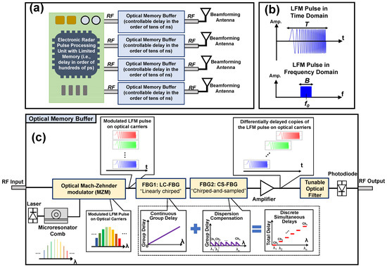
Figure 1.
(a) An envisioned hybrid optoelectronic beamforming radar system sending LFM pulses. Due to limited memory, the electronic radar processing unit can add only a small delay in the order of hundreds of picoseconds. In contrast, the optical memory buffer can add delays of tens of nanoseconds. (b) Depiction of the LFM pulse used in radar systems in the time domain and frequency domain. (c) The proposed optical memory buffer structure. An input RF-LFM pulse modulates optical carriers from a Kerr comb. The modulated carriers are sent through a concatenation of LC-FBG and CS-FBG. The amount of added wavelength-dependent delay is selected using a tunable optical filter, and the signal is converted to the RF domain using a photodiode.
This paper focuses on the performance of the optical memory buffer composed of a Kerr comb and concatenated off-the-shelf chirped FBGs. The radar processor generates the RF-LFM pulse using the mathematical model:
where is the RF center frequency, B is the total bandwidth of the RF signal (in Hz), and T is the pulse duration [29]. During the pulse duration , the instantaneous frequency linearly scans the range . In the frequency domain, the pulse is expressed as:
Figure 1b shows the LFM pulse in the time and frequency domains. Figure 1c focuses on the optical memory buffer, the primary research objective of this study. The RF-LFM pulse is fed into the optical memory buffer. In the optical Mach–Zehnder modulator (MZM), the RF-LFM pulse is modulated onto optical carriers from a microresonator Kerr comb at different wavelengths (’s), creating several copies of the LFM pulse on different optical carriers.
These optical copies are sent into a linearly chirped FBG (FBG1: LC-FBG), which provides a continuous wavelength-dependent group delay with added intra-channel group-delay dispersion. The added dispersion is then removed by a chirped-and-sampled FBG (FBG2: CS-FBG), compensating for the dispersion of multiple equally spaced frequency channels simultaneously. At the output of the concatenated FBGs, different copies of the input are available for detection, where each wavelength carrier corresponds to a signal with a different delay. The signal copies are amplified, and a tunable optical filter selects the added optical delay. The output is converted back to the RF domain using a photodiode. In summary, the four essential components of the optical memory buffer system are (i) FBG1, (ii) FBG2, (iii) optical amplifier, and (iv) optical tunable filter.
To theoretically explain the processes of adding the delay and compensating for the chromatic dispersion, let us assume we start from the Kerr comb in the angular frequency domain [30] (for the remaining part of this section, we will switch from the frequency domain (f) to angular frequency domain () notation to make the subsequent analysis consistent with the literature):
where is the repetition rate in the angular frequency domain, corresponding to the free spectral range (FSR) of the comb, and represents the amplitude of the mth spectral line. Let us assume that the signal passes through the optical Mach–Zehnder modulator to amplitude modulate the RF-LFM pulse signal onto all the Kerr comb carriers, where:
such that is the bandwidth in terms of the angular frequency. This will produce the modulated signal:
where is an amplitude modulation coefficient, and ∗ is the convolution operator. When passes through the concatenation of FBGs while ignoring frequency-independent loss, we obtain the FBGs output signal as:
where the medium’s optical properties determine the functional dependence of on . Since, normally, , it is valid to describe by the first few terms of its Taylor expansion around [31]:
Therefore:
The first term, , represents a phase term of no importance to intensity-based systems, such as ours. The second term, having an exponent that is linearly dependent on , stands for a pure delay:
where and are the group delay and group velocity at the carrier frequency , respectively. The third term of Equation (8) shows a quadratic dependence on , resulting in pulse distortion.
A linearly chirped FBG (LC-FBG) comprises a continuously written fiber Bragg grating of length (), with a continuous linearly increasing (or decreasing) period, which covers a spectral segment, . Thus, for positive chirping, where shorter wavelengths have less delays than longer ones, the dependence of the delay on the center frequency of a pulse propagating through the LC-FBG is given by:
where:
and while ignoring , this yields:
The fact that the device has frequency dependence delay means it has dispersion, so its gives rise to pulse distortion.
On the other hand, a chirped-and-sampled FBG (CS-FBG) dispersion compensator is a short device that offers the same amount of constant delay to the angular frequencies at the center of the CS-FBG channels , where is the first central angular frequency carrier in the ITU grid, , and is the ITU grid frequency spacing. Thus, the CS-FBG effect on the group delay at the frequencies ’s could be neglected as it is independent of . Also, the device has a pre-designed dispersion at the frequencies belonging to the ITU grid opposing those of the LC-FBG:
Therefore, the overall optical transfer function of the concatenation of the two FBGs at the ’s is , which is simply a delay-only element with no dispersion for carrier frequencies populating the ITU grid. After passing through the amplifier with the gain (G) and selecting the frequency of the desired delayed signal in the filter, the output selected signal becomes:
So by selecting the signal on the frequency modulated on the mth comb carrier, while holds, one can define the amount of added delay using the system using Equation (13). And the selected optical signal in the time domain becomes the inverse Fourier transform of .
3. Experimental Setup
The experimental setup for the optical memory buffer is shown in Figure 2a. Multiple frequency carriers are generated using a microresonator [27]. The microresonator consists of a silicon nitride (Si3N4) waveguide with a cross-section of 1.5 m × 0.9 m, and a ring radius of ∼119 m. The waveguide is pumped using an external cavity laser diode (ECDL) at 1559 nm light in the anomalous dispersion region, with coupled input power to the waveguide of 32.5 dBm. The resonator’s corresponding quality (Q) factor and the cavity linewidth are and 150 MHz, respectively. Figure 2b shows the spectrum of the generated soliton Kerr comb using the microresonator. The generated comb’s free spectral range (FSR) is ∼192 GHz. A zoomed-in view of the comb frequency lines over the optical C-band (1527.7–1567.6 nm) is shown in Figure 2c, where the measured power of the carriers next to the pump is −10 dBm, and the OSNR values of the carriers ranged between 18–31 dB (at 0.05 nm optical spectrum analyzer resolution).
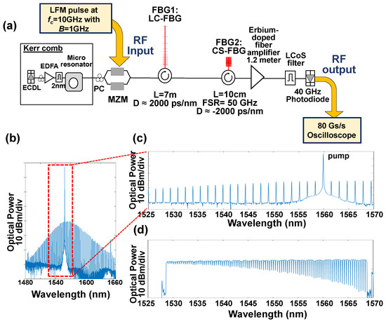
Figure 2.
(a) The experimental setup of the optical memory buffer for delaying a linear frequency-modulated wide-band pulse using carriers from a Kerr comb and off-the-shelf LC-FBG and CS-FBG. We modulate the LFM pulse on optical Kerr comb carriers and send the signal through a concatenation of LC-FBG and CS-FBG. (b) The optical spectrum of the generated soliton Kerr comb using the microresonator. (c) A zoomed-in spectrum for the Kerr comb carriers in the C-band (1527.7–1567.6 nm). (d) The spectrum of the light reflection from the concatenation of the FBGs.
The comb carriers are double-sideband modulated with the LFM signal using a communication-grade Mach–Zehnder modulator (MZM) (40+ Gb/s Intensity Modulator, Eospace, WA, USA), biased at the quadrature. The modulated carriers are then sent to FBG1 (LC-FBG) and FBG2 (CS-FBG). The 7 m functional section of FBG1 emulates continuous dispersion of approximately 2000 ps/nm over the C-band, whereas FBG2 performs its dispersion-compensating function for all the C-band channels belonging to the 50 GHz ITU grid. Both FBGs are off-the-shelf items, and the combined insertion loss is ∼7 dB. The optical signals are amplified in a specially ordered 22 dB gain erbium-doped fiber amplifier (EDFA) with 1.2 m effective length to minimize latency. Next, a tunable liquid crystal on silicon (LCoS) optical filter (WaveShaper 1000S, FINISAR, Sunnyvale, CA, USA) is used to select the wavelength channel of interest, corresponding to the desired delay of the tunable optical memory buffer. Finally, we convert the signal to the RF domain using a 40 GHz photodiode.
Figure 2d shows the optical spectrum of the concatenation of the LC-FBG and the CS-FBG when we illuminate the concatenation of the FBGs with a broadband optical source. We observe the reflected 100 accessible optical channels having 50 GHz spacing. Since the CS-FBG is sampled chirping yields 100 channels, while the LC-FBG is chirped over a length of 7 m with a round trip-trip delay associated with it, it should be assumed that every channel will have ns compared to its neighboring one.
4. Characterization of the Optical Memory Buffer
We carry out the characterization by (i) measuring the delay tuning range, (ii) measuring the latency of the system, and (iii) measuring the bandwidth of the delay channels.
4.1. Measuring the Delay Tuning Range
We start our characterization by measuring the added delay for each of the FBG channels using an electrical vector network analyzer as shown in Figure 3a. We send the electrical vector analyzer waveform to the RF input of the optical memory buffer. We modulate the waveform on a tunable laser source carrier and analyze the waveform phase at the buffer output. We deduce the delay from the slope of the phase curve for each wavelength channel compared to the zero wavelength of the optical channel at nm. Figure 3b shows the measured delay values and the delay trendline. We observe that the range of optical channels over 1527.7–1567.9 nm spans 76 ns, giving each of the 100 channels ∼0.76 ns of additional delay compared to its left-sided wavelength channel.
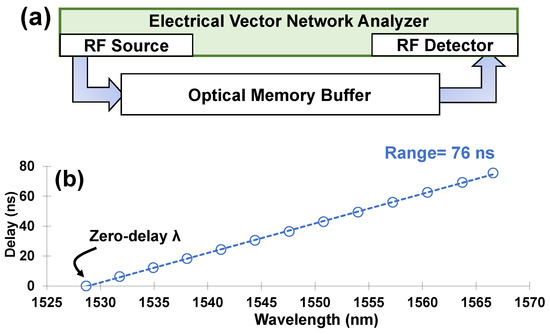
Figure 3.
(a) The configuration for measuring the wavelength-dependent delay in the optical memory buffer induced by the concatenation of off-the-shelf LC-FBG and CS-FBG. A waveform from an electrical vector network analyzer (VNA) is sent from the RF input port of the optical memory buffer. The output is retrieved in the VNA, and the delay is measured by analyzing the phase waveform. (b) The delay curve of the optical memory buffer. We observe a delay tuning range of 76 ns over the wavelength range of 1527.7 nm to 1567.9 nm.
4.2. Characterizing the Latency of the Delay System
We characterize the induced latency (i.e., non-functional added delay) by each of the components in the system: (i) FBG1, (ii) FBG2, (iii) optical amplifier (EDFA), and (iv) tunable LCoS optical filter. The measurement is performed by connecting only one optical component between the optical modulator and photodiode in the optical memory buffer and characterizing the vector network analyzer waveform after transmitting the signal through the component. The results are presented in Table 1. The first column in the table represents the optical component under test. The second column describes the internal element causing the latency. We observe that most of the measured latency is due to the wiring fibers connecting the different components inside the off-the-shelf item, which could be minimized if the components are carefully packaged. The third column presents the measured values of the latency at = 1527.27 nm (zero-delay ). The fourth column shows the minimum possible latency for the element if the internal fiber jumpers are eliminated or shortened.

Table 1.
Latency for the components in the optical delay system.
The effective length of FBG1, contributing to the tuning of the delay range, is 7 m, while the effective length of FBG2 is 10 cm. The measured latency induced by the combination of FBG1 and FBG2 at the zero-delay is in the order of ∼155 ns, which we believe is due to the internal circulator connectors and fiber jumpers linking between the device port and FBG; through proper packaging, this latency can be eliminated to below 1.5 ns. The optical amplifier (EDFA) used has a functional length of 1.2 m, and the functional length of the LCoS filter is determined by the distance between the collimators and the internal spatial light modulator, which is in the order of centimeters. Therefore, we estimate that the optical buffer latency can potentially be reduced to less than 5 ns by eliminating the sources of latency. This assumption entails that the wiring fibers for each component are no longer than 20 cm.
4.3. Characterizing the Bandwidth of the Delay Channels
In Figure 4, we measure the magnitude and phase response of the FBG channels in the optical memory buffer system to characterize their bandwidth [32]. The measurement configuration is shown in Figure 4a. We connect a swept-laser-based all-optical vector network analyzer between the ports of the concatenation of the FBGs. We characterize 12 out of the 100 wavelength delay channels, and the results are shown in Figure 4b,c. In Figure 4b, we observe that the 3 dB bandwidth of the FBG channels can at least span the frequency range from −22.7 to +21.7 GHz (i.e., the 3 dB bandwidth is at least ±20 GHz). Also, the results of Figure 4c show that the phase deviation is between −1.67 and +1.32 rad over the ±20 GHz bandwidth.
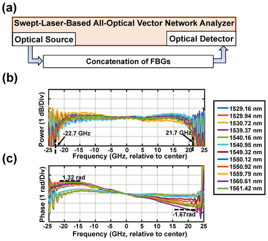
Figure 4.
(a) Experimental configuration to characterize the magnitude and phase response of the optical memory buffer system using a swept-laser-based optical vector network analyzer (OVA). (b) Magnitude response of different delayed wavelength channels of the delay system. (c) Phase response of different wavelength channels of the delay system.
We further extend the investigation and measure the RF system bandwidth using the VNA. We use the same setup of Figure 3a, where we set the VNA to measure the magnitude response for the optical memory buffer when the signal passes through (i) only the LC-FBG in Figure 5a, (ii) only the CS-FBG in Figure 5b, and (iii) the entire optical buffer system composed of the concatenation of FBGs in Figure 5c. As a proof of concept, we show the results for the delayed channel at 1550.12 nm. As can be observed from these figures, using the LC-FBG causes the system to suffer from frequency nulls induced by the fading of chromatic dispersion, and the same behavior is observed from the CS-FBG RF magnitude response. Meanwhile, the combination of FBGs eliminates the added fading and provides a flat magnitude response for frequency ranges higher than 20 GHz, enabling the system to delay large bandwidth signals.
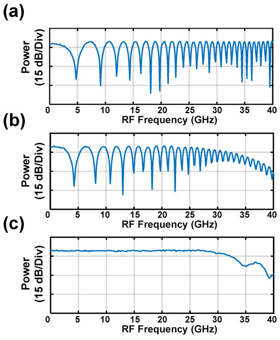
Figure 5.
Experimental results for measuring the RF magnitude response of the optical buffer using the VNA when the delay system is made of (a) only the LC-FBG, (b) only the CS-FBG, and (c) the combination of LC-FBG and CS-FBG.
5. Experimentally Measuring the PSL of LFM Pulse
In this section, we experimentally investigate the PSL performance of the LFM pulse after delaying multiple copies of an LFM pulse using the optical memory buffer. The following subsections include explaining the hardware used for RF-LFM pulse generation and detection, explaining the signal processing for measuring the PSL of an LFM pulse, measuring the PSL performance of the LFM pulse, and comparing the optical memory buffer performance to the system made up of discrete lasers.
5.1. Configuration for RF-LFM Pulse Generation and Detection
The hardware configuration for generating an RF-LFM pulse and detecting it is shown in Figure 6a. The LFM pulse is generated from a 12-bit 92 GSample/sec waveform generator. The LFM pulse has a bandwidth of B = 1 GHz at a center frequency of = 10 GHz. The pulse duration is T = 3 s at a repetition rate of 250 kHz. The pulse is captured using a 10-bit 80 GSample/sec oscilloscope. Figure 6b shows the captured LFM pulse in the time domain, and Figure 6c shows the LFM pulse in the frequency domain.
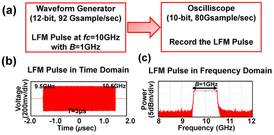
Figure 6.
(a) Experimental configuration for back-to-back generation and detection of an LFM pulse at 10 GHz center frequency and with 1 GHz bandwidth. (b) The captured LFM pulse in the time domain. (c) The captured LFM pulse in the frequency domain.
5.2. The Process of Measuring the PSL
To measure the PSL, we follow the steps in Figure 7a. The process involves [3]: (i) Fourier transformation of the received pulse, (ii) removal of the quadratic phase by multiplying the pulse Fourier transform by , (iii) multiplication by a Hamming window to achieve a peak having a 3 dB width of and a PSL of 42.68 dB, and finally, (iv) inverse Fourier transformation of the result.
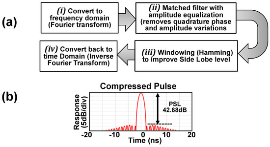
Figure 7.
(a) The process of measuring the PSL of a compressed pulse. (b) The ideal LFM pulse of B = 1 GHz at = 10 GHz after compression shows the maximum PSL to be 42.68 dB in the back-to-back configuration.
When we perform the PSL measurement process on our LFM pulse of B = 1 GHz at = 10 GHz that is recorded in the electronic back-to-back configuration, we obtain a PSL of 42.68 dB as shown in Figure 7b.
5.3. Experimentally Measuring the PSL Performance of the LFM Pulse after Delaying It Using the Optical Memory Buffer
We experimentally measure the PSL performance of the LFM pulse after delaying it using the optical memory buffer. We feed the optical memory buffer with the LFM signal at the RF input port and capture the delayed signal at the buffer output using the optical spectrum analyzer as shown in Figure 8a. Given that our comb FSR is approximately 192 GHz and not fully aligned with the 50 GHz ITU grid, we concentrate on three comb line carriers in the vicinity of the CS-FBG center frequencies at 1535.43 nm, 1545.72 nm, and 1556.55 nm as illustrated in Figure 8b, to ensure that the LFM pulse is fully contained in the flat magnitude response region of the channel. We select these channels because we assume the microresonator can be fabricated in any desired dimensions and FSR to exactly match the CS-FBGs, while the currently available devices may be sufficient for proof of concept. We individually select each channel using the tunable filter and detect the channel using the photodiode of the optical memory buffer.
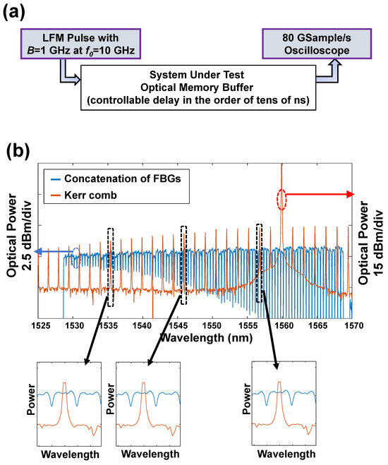
Figure 8.
(a) Setup for measuring the PSL of an LFM pulse that is delayed using the optical memory buffer. (b) The selected wavelengths from the Kerr comb source, where each wavelength carrier represents a different delay value.
In our assessment, we start by measuring the PSL for the LFM pulse at the output of the optical buffer when we bypass the FBGs. The compressed pulses’ results are shown in Figure 9a, with PSL values of ∼35 dB (lower than the RF back-to-back 42.67 dB baseline), indicating the non-flatness of the modulator and detector frequency response when bypassing the delaying FBGs. Next, we design an offline digital filter to compensate for this non-flatness of the system response for every optical delay channel. We apply this filter to the detected signal, and the result of the compressed pulse shows obtaining an ideal PSL of 42.68 dB, as in Figure 9b, representing an improvement of 6.45–8.76 dB. Afterward, we insert the FBGs into our optical memory buffer system and measure the PSL. Our results in Figure 9c show PSL values of 34.43–35.45 dB for the compressed LFM pulse after delay, indicating an overall penalty in the PSL of 7.23–8.25 dB.
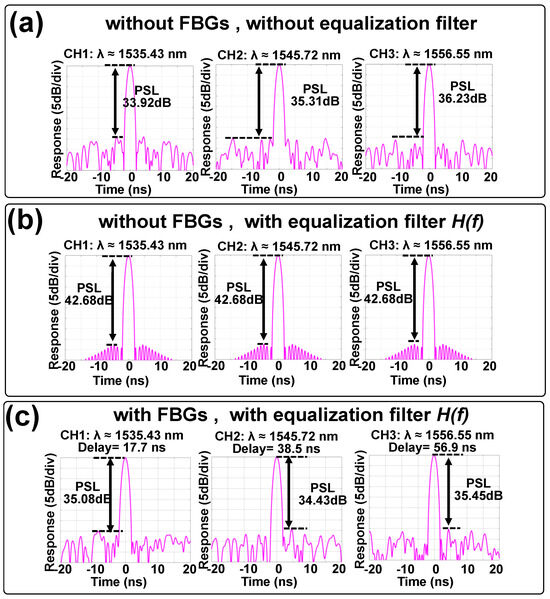
Figure 9.
(a) The PSL for three versions of the LFM pulse after compression when the FBGs are bypassed in the optical delay buffer. (b) The PSL for three delayed versions of the LFM pulse after compression and after using the equalization filter . (c) The PSL for three delayed versions of the LFM pulse after compression when inserting the FBGs for the delay and using the equalization filter .
5.4. Performance Comparison with the Buffer Made of a Bank of Lasers
For performance comparison, we replace the Kerr comb with four discrete laser sources. In Figure 10a, we show the modified setup of the optical memory buffer, where we use four lasers with <10 kHz linewidth (Teraxion TNL). The lasers are set to the wavelengths of 1540.16 nm, 1544.92 nm, 1549.72 nm, and 1554.54 nm as shown in Figure 10b. Every laser emits ∼10 dBm of optical power with more than 35 dB of optical OSNR. We repeat the same systematic analysis of the prior subsection for penalty analysis.
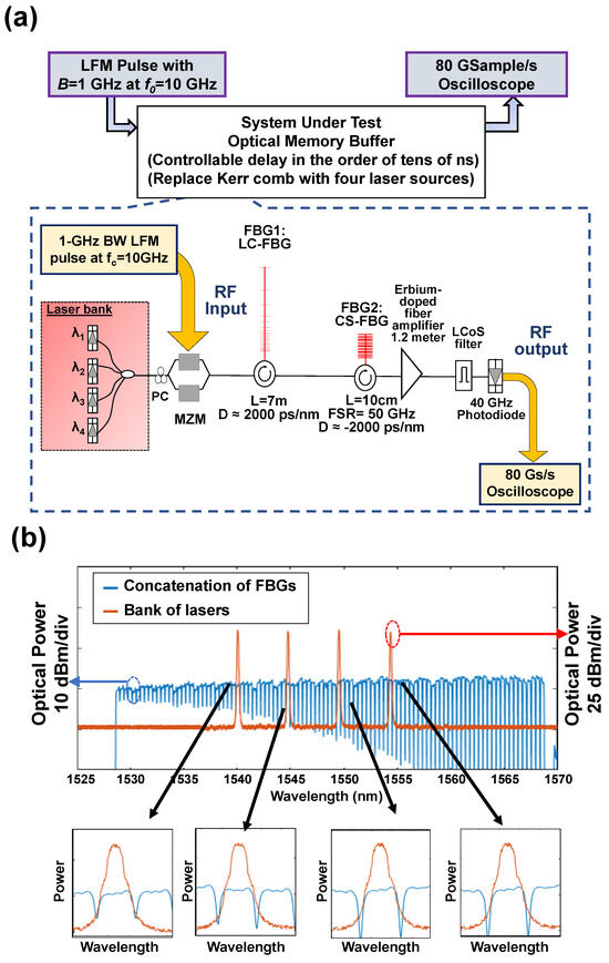
Figure 10.
(a) The modified setup for measuring the PSL of an LFM pulse that is delayed using the optical buffer. (b) The spectrum of the FBG delay channels and the wavelengths of the laser carriers.
In Figure 11a, we measure the PSL of the LFM pulses when we send the signal through the optical buffer while bypassing the FBGs. The measured PSL values are 36.78–37.43 dB due to the non-flat frequency response of the optical system of the modulator and detector. We design a digital filter for each channel and apply the filter. The PSL values become similar to the baseline at 42.68 dB as shown in Figure 11b. Then, we insert the FBGs into the optical buffer system and measure the PSL as in Figure 11c. The measured PSL values range between 41.11 and 41.32 dB for the delayed pulses, indicating a PSL penalty of only 1.36–1.57 dB.
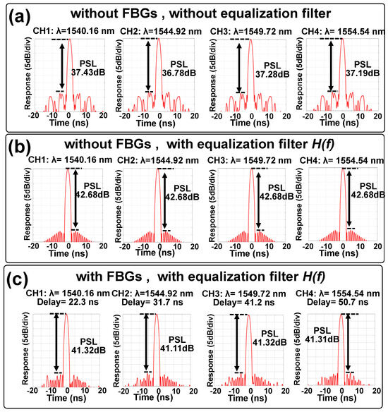
Figure 11.
The results when we replace the Kerr comb carriers with a bank of lasers. (a) The PSL for the four versions of the LFM pulse after compression when the FBGs are bypassed in the optical delay buffer. (b) The PSL for the four versions of the LFM pulse after compression and after using the equalization filter . (c) The PSL for the four delayed versions of the LFM pulse after compression when inserting the FBGs for the delay and using the equalization filter .
For further analysis, we investigate increasing the LFM pulse bandwidth to 10 GHz at a center frequency of 5 GHz (10 times greater bandwidth than the precedent experiment). This study could validate the benefit of concatenating the LC-FBG and CS-FBG. Here, we repeat the systematic analysis approach, where in Figure 12a,b, we show the captured 10 GHz bandwidth LFM pulse experimentally in the time and frequency domains in the back-to-back RF configuration. In Figure 12c, we show the compressed pulse in the back-to-back configuration after applying a matched filter and windowing, where the compressed pulse shows a PSL of 42.68 dB. Figure 12c–e show the PSL when we send the signal through the optical memory buffer while bypassing the FBGs, the PSL when we insert the FBGs into the optical buffer system, and the PSL when we design and apply the digital filter . The results in Figure 12e show that the system can potentially be used to delay broadband signals with a penalty of 3.95–6.7 dB.
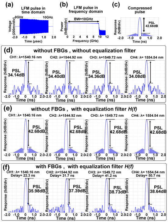
Figure 12.
The results when delaying a 10 GHz bandwidth LFM pulse at a center frequency of 5 GHz. (a) The captured LFM pulse in the time domain. (b) The captured LFM pulse in the frequency domain. (c) The back-to-back (i.e., ideal) LFM pulse of B = 10 GHz at = 5 GHz after compression, showing a maximum PSL of 42.68 dB. (d) The PSL for the four versions of the LFM pulse in the optical delay buffer after compression when the FBGs are bypassed. (e) The PSL for the four versions of the LFM pulse after compression and after using the equalization filter . (f) After compression, the PSL for the four delayed versions of the LFM pulse when inserting the FBGs for the delay and using the equalization filter .
6. Discussion and Conclusions
In conclusion, we have demonstrated delaying a radio frequency–linear frequency-modulated (LFM) wide-band pulse of 1-GHz bandwidth by modulating the LFM pulse on optical carriers from a Kerr comb and sending the modulated carriers through an optical memory buffer system with the concatenation of off-the-shelf linearly chirped fiber Bragg grating (LC-FBG) and chirped-and-sampled FBG (CS-FBG). Potential advantages of using our structure include (i) a larger tunable delay range, (ii) low latency, (iii) wide bandwidth, and (iv) high PSL.
Our measurements show that our proposed system can potentially (i) provide a delay range of 76 ns with 100 steps, (ii) delay the signal with a latency of <5 ns if carefully packaged, (iii) delay the signals with bandwidth up to ±20 GHz, and (iv) achieve PSL values of 34.43–35.45 dB.
When we analyze the system’s performance when replacing the Kerr comb source with separate lasers, the results show that independent laser sources demonstrate better PSL performance, which may be attributed to the higher emitted power per carrier compared to the comb, the higher OSNR per carrier, and the smaller number of carriers that become boosted in the 1.2 m amplifier. Here, we note that the power of the Kerr comb frequency lines and the quality of OSNR depend on several factors, including the power level of the pump laser and its carrier-to-noise ratio [28]. On the other hand, although independent laser sources show better performance, using these may not be considered a scalable solution, as they require independent packaging and separate controllers for each laser.
Therefore, we believe the performance of the optical buffer using the Kerr comb should be improved in the future by (i) aligning the Kerr comb and the FBGs spectra by redesigning the ring resonator to match the FBGs or vice versa, (ii) optimizing the generation of the Kerr comb with higher OSNR and power levels, and (iii) stabilizing the temperature of the Kerr comb source for better frequency/phase stability. For example, aligning the Kerr comb to the FBG can be achieved in the design and fabrication phase by tuning the microresonator’s physical dimensions and its dispersion properties [33,34]. In addition, after the fabrication, one could slightly tune the Kerr comb FSR by implementing external thermal tuning or mechanical stress [35,36]. Also, the mechanical and thermal approaches may tune the FBGs to align with the generated comb as previously reported in [37,38]. Regarding the Kerr comb power level and its OSNR, one should consider maximizing the input coupled power of the device [33] and using a low noise amplifier right after the device to increase the carrier’s power levels. Although we did not observe significant effects of the temperature variation on the comb generation in the lab environment, it is essential to note that severe variation may lead the microresonator to lose its soliton state or slightly induce frequency shift, leading the carriers to lose the alignment with the center of the FBGs which impacts the RF channel bandwidth magnitude response.
Although redesigning the Kerr comb to meet our application requirements may take a long turnaround time, the current results indicate that compared to the independent lasers, the reduction in the optical carrier power from +10 dBm to −10 dBm and decreased OSNR from <35 dB to <31 dB for the Kerr comb carriers lead to increased penalty from ∼1 dB to 7–8 dB for the LFM pulse with 1 GHz of bandwidth. One potential solution to address this issue would be, for example, using non-solitonic combs, which demonstrate higher pump-to-comb conversion efficiency and high power-per-line [39]. Moreover, by extending our analysis by increasing the LFM pulse bandwidth by a factor of 10 from 1 GHz to 10 GHz, we can conclude that the minimum penalty would increase from ∼1 dB to 4–6 dB.
In our concept demonstration, one can observe that the actual latency greatly exceeds the minimum viable one. This added latency is due to using off-the-shelf components with long internal fiber jumpers connecting the elements. Luckily, most of the components have the potential to be integrated into a single photonic integrated circuit. For example, the chirped gratings are designed and fabricated on-chip [40,41,42]. Moreover, the amplifier can be replaced with an integrated semiconductor optical amplifier [43,44]. In addition, the LCoS filter can be replaced with any integrated photonic technology filter such as ring resonator tunable filters [45,46].
Author Contributions
Conceptualization, A.A. and M.T.; methodology, A.A., Y.C. and M.T.; software, A.A. and M.T.; validation, A.A., Y.C. and M.T.; formal analysis A.A. and M.T.; investigation, A.A. and M.T.; resources, P.L. and A.W.; data curation, A.A. and M.T.; writing—original draft preparation, A.A.; writing—review and editing, A.W. and M.T.; visualization, A.A. and M.T.; project administration, M.T. All authors have read and agreed to the published version of the manuscript.
Funding
Center for Integrated Access Network (CIAN) (Y501119); and National Science Foundation (NSF) (ECCS-1202575); Defense Security Cooperation Agency (DSCA) (4440646262); The Office of Naval Research (ONR) (N000141812352).
Institutional Review Board Statement
Not applicable.
Informed Consent Statement
Not applicable.
Data Availability Statement
Underlying the results presented in this paper are not publicly available at this time but may be obtained from the authors upon reasonable request.
Acknowledgments
The authors would like to thank Fatemeh Alishahi, Amirhossein Mohajerin-Ariaei, Long Li, and Kaiheng Zhou.
Conflicts of Interest
The authors declare no conflicts of interest.
References
- Yang, D.H.; Lin, W.P. Phased-array beam steering using optical true time delay technique. Opt. Commun. 2015, 350, 90–96. [Google Scholar] [CrossRef]
- Tan, M.; Xu, X.; Wu, J.; Morandotti, R.; Mitchell, A.; Moss, D.J. Photonic RF and microwave filters based on 49 GHz and 200 GHz Kerr microcombs. Opt. Commun. 2020, 465, 125563. [Google Scholar] [CrossRef]
- Rotman, R.; Tur, M.; Yaron, L. True time delay in phased arrays. Proc. IEEE 2016, 104, 504–518. [Google Scholar] [CrossRef]
- Urick, V.J.; Williams, K.J.; McKinney, J.D. Fundamentals of Microwave Photonics; John Wiley & Sons: Hoboken, NJ, USA, 2015. [Google Scholar]
- Zhou, P.; Zhang, F.; Pan, S. Generation of linear frequency-modulated waveforms by a frequency-sweeping optoelectronic oscillator. J. Light. Technol. 2018, 36, 3927–3934. [Google Scholar] [CrossRef]
- Klinger, O.; Stern, Y.; Pederiva, F.; Jamshidi, K.; Schneider, T.; Zadok, A. Continuously variable long microwave-photonic delay of arbitrary frequency-chirped signals. Opt. Lett. 2012, 37, 3939–3941. [Google Scholar] [CrossRef] [PubMed]
- Min, S.S.; Yoo, H.; Won, Y.H. Time–wavelength hybrid optical CDMA system with tunable encoder/decoder using switch and fixed delay-line. Opt. Commun. 2003, 216, 335–342. [Google Scholar] [CrossRef]
- Yoo, S.B. Optical packet and burst switching technologies for the future photonic internet. J. Light. Technol. 2006, 24, 4468–4492. [Google Scholar] [CrossRef]
- Liu, Y.; Hill, M.; Geldenhuys, R.; Calabretta, N.; De Waardt, H.; Khoe, G.D.; Dorren, H. Demonstration of a variable optical delay for a recirculating buffer by using all-optical signal processing. IEEE Photonics Technol. Lett. 2004, 16, 1748–1750. [Google Scholar] [CrossRef]
- Tucker, R.S. The role of optics and electronics in high-capacity routers. J. Light. Technol. 2006, 24, 4655–4673. [Google Scholar] [CrossRef]
- Praena, J.Á.; Carballar, A. Chirped Integrated Bragg Grating Design. Photonics 2024, 11, 476. [Google Scholar] [CrossRef]
- Zou, X.H.; Pan, W.; Luo, B.; Qin, Z.M.; Wang, M.Y.; Zhang, W.L. Periodically chirped sampled fiber Bragg gratings for multichannel comb filters. IEEE Photonics Technol. Lett. 2006, 18, 1371–1373. [Google Scholar] [CrossRef]
- Asseh, A.; Storoy, H.; Sahlgren, B.E.; Sandgren, S.; Stubbe, R.A. A writing technique for long fiber Bragg gratings with complex reflectivity profiles. J. Light. Technol. 1997, 15, 1419–1423. [Google Scholar] [CrossRef]
- Zeitouny, A.; Stepanov, S.; Levinson, O.; Horowitz, M. Optical generation of linearly chirped microwave pulses using fiber Bragg gratings. IEEE Photonics Technol. Lett. 2005, 17, 660–662. [Google Scholar] [CrossRef]
- Ashrafi, R.; Park, Y.; Azana, J. Fiber-based photonic generation of high-frequency microwave pulses with reconfigurable linear chirp control. IEEE Trans. Microw. Theory Tech. 2010, 58, 3312–3319. [Google Scholar] [CrossRef]
- Ghelfi, P.; Scotti, F.; Laghezza, F.; Bogoni, A. Photonic generation of phase-modulated RF signals for pulse compression techniques in coherent radars. J. Light. Technol. 2012, 30, 1638–1644. [Google Scholar] [CrossRef]
- Moslemi, P.; Chen, L.R. Simultaneously generating multiple chirped microwave pulses with superimposed FBGs. IEEE Photonics Technol. Lett. 2017, 29, 1387–1390. [Google Scholar] [CrossRef]
- Wang, H.; Wu, B.; Zhou, H.; Wang, W.; Xu, G. Optical Tunable Frequency-Doubling OEO Using a Chirped FBG Based on Orthogonally Polarized Double Sideband Modulation. Photonics 2023, 10, 1002. [Google Scholar] [CrossRef]
- Jiang, Y.; Howley, B.; Shi, Z.; Zhou, Q.; Chen, R.T.; Chen, M.Y.; Brost, G.; Lee, C. Dispersion-enhanced photonic crystal fiber array for a true time-delay structured X-band phased array antenna. IEEE Photonics Technol. Lett. 2004, 17, 187–189. [Google Scholar] [CrossRef]
- Shaheen, S.; Gris-Sánchez, I.; Gasulla, I. True-time delay line based on dispersion-flattened 19-core photonic crystal fiber. J. Light. Technol. 2020, 38, 6237–6246. [Google Scholar] [CrossRef]
- Zhao, Y.; Wang, C.; Zhao, Z.; Zhang, W.; Liu, J. A Microwave Photonics True-Time-Delay System Using Carrier Compensation Technique Based on Wavelength Division Multiplexing. Photonics 2023, 10, 34. [Google Scholar] [CrossRef]
- Sun, Q.; Liu, C.; Yang, J.; Liu, J.; Dong, J.; Li, W. Phase-Derived Ranging Based Fiber Transfer Delay Measurement Using a Composite Signal for Distributed Radars with Fiber Networks. Photonics 2023, 10, 421. [Google Scholar] [CrossRef]
- Zhou, W.; Stead, M.; Weiss, S.; Okusaga, O.; Jiang, L.; Anderson, S.; Huang, Z.R. Developing an integrated photonic system with a simple beamforming architecture for phased-array antennas. Appl. Opt. 2017, 56, B5–B13. [Google Scholar] [CrossRef]
- Xu, X.; Tan, M.; Wu, J.; Morandotti, R.; Mitchell, A.; Moss, D.J. Microcomb-Based Photonic RF Signal Processing. IEEE Photonics Technol. Lett. 2019, 31, 1854–1857. [Google Scholar] [CrossRef]
- Hu, J.; He, J.; Liu, J.; Raja, A.S.; Karpov, M.; Lukashchuk, A.; Kippenberg, T.J.; Brès, C.S. Reconfigurable radiofrequency filters based on versatile soliton microcombs. Nat. Commun. 2020, 11, 4377. [Google Scholar] [CrossRef] [PubMed]
- Anashkina, E.A.; Marisova, M.P.; Andrianov, A.V.; Akhmedzhanov, R.A.; Murnieks, R.; Tokman, M.D.; Skladova, L.; Oladyshkin, I.V.; Salgals, T.; Lyashuk, I.; et al. Microsphere-Based Optical Frequency Comb Generator for 200 GHz Spaced WDM Data Transmission System. Photonics 2020, 7, 72. [Google Scholar] [CrossRef]
- Xu, X.; Wu, J.; Nguyen, T.G.; Shoeiby, M.; Chu, S.T.; Little, B.E.; Morandotti, R.; Mitchell, A.; Moss, D.J. Advanced RF and microwave functions based on an integrated optical frequency comb source. Opt. Express 2018, 26, 2569–2583. [Google Scholar] [CrossRef]
- Liao, P.; Bao, C.; Kordts, A.; Karpov, M.; Pfeiffer, M.H.; Zhang, L.; Cao, Y.; Almaiman, A.; Mohajerin-Ariaei, A.; Alishahi, F.; et al. Effects of erbium-doped fiber amplifier induced pump noise on soliton Kerr frequency combs for 64-quadrature amplitude modulation transmission. Opt. Lett. 2018, 43, 2495–2498. [Google Scholar] [CrossRef] [PubMed]
- Raz, O.; Barzilay, S.; Rotman, R.; Tur, M. Submicrosecond scan-angle switching photonic beamformer with flat RF response in the C and X bands. J. Light. Technol. 2008, 26, 2774–2781. [Google Scholar] [CrossRef][Green Version]
- Kippenberg, T.J.; Holzwarth, R.; Diddams, S.A. Microresonator-based optical frequency combs. Science 2011, 332, 555–559. [Google Scholar] [CrossRef]
- Pan, Z.; Song, Y.; Yu, C.; Wang, Y.; Yu, Q.; Popelek, J.; Li, H.; Li, Y.; Willner, A.E. Tunable chromatic dispersion compensation in 40-Gb/s systems using nonlinearly chirped fiber Bragg gratings. J. Light. Technol. 2002, 20, 2239–2246. [Google Scholar] [CrossRef]
- Almaiman, A.; Cao, Y.; Alishahi, F.; Fallahpour, A.; Li, L.; Liao, P.; Zou, K.; Zach, S.; Cohen, N.; Tur, M.; et al. Experimental Characterization of Low-Latency Multiple and Tunable Delays of Wideband Analog LFM Signal Using Concatenated Linearly Chirped and Sampled FBGs. In Proceedings of the CLEO: Science and Innovations. Optica Publishing Group, San Jose, CA, USA, 15–20 May 2019; p. SF2N–3. [Google Scholar]
- Liu, Y.; Xuan, Y.; Xue, X.; Wang, P.H.; Chen, S.; Metcalf, A.J.; Wang, J.; Leaird, D.E.; Qi, M.; Weiner, A.M. Investigation of mode coupling in normal-dispersion silicon nitride microresonators for Kerr frequency comb generation. Optica 2014, 1, 137–144. [Google Scholar] [CrossRef]
- Kim, S.; Han, K.; Wang, C.; Jaramillo-Villegas, J.A.; Xue, X.; Bao, C.; Xuan, Y.; Leaird, D.E.; Weiner, A.M.; Qi, M. Dispersion engineering and frequency comb generation in thin silicon nitride concentric microresonators. Nat. Commun. 2017, 8, 372. [Google Scholar] [CrossRef] [PubMed]
- Feng, Y.; Zheng, Y.; Zhang, F.; Yang, J.; Qin, T.; Wan, W. Passive fine-tuning of microcavity whispering gallery mode for nonlinear optics by thermo-optical effect. Appl. Phys. Lett. 2019, 114, 101103. [Google Scholar] [CrossRef]
- Jin, W.; Polcawich, R.G.; Morton, P.A.; Bowers, J.E. Piezoelectrically tuned silicon nitride ring resonator. Opt. Express 2018, 26, 3174–3187. [Google Scholar] [CrossRef]
- Han, Y.G.; Dong, X.; Lee, J.; Lee, S. Simultaneous measurement of bending and temperature based on a single sampled chirped fiber Bragg grating embedded on a flexible cantilever beam. Opt. Lett. 2006, 31, 2839–2841. [Google Scholar] [CrossRef] [PubMed]
- Sun, J.; Dai, Y.; Chen, X.; Zhang, Y.; Xie, S. Thermally tunable dispersion compensator in 40-Gb/s system using FBG fabricated with linearly chirped phase mask. Opt. Express 2006, 14, 44–49. [Google Scholar] [CrossRef]
- Rizzo, A.; Daudlin, S.; Novick, A.; James, A.; Gopal, V.; Murthy, V.; Cheng, Q.; Kim, B.Y.; Ji, X.; Okawachi, Y.; et al. Petabit-scale silicon photonic interconnects with integrated kerr frequency combs. IEEE J. Sel. Top. Quantum Electron. 2022, 29, 1–20. [Google Scholar] [CrossRef]
- Strain, M.J.; Sorel, M. Design and fabrication of integrated chirped Bragg gratings for on-chip dispersion control. IEEE J. Quantum Electron. 2010, 46, 774–782. [Google Scholar] [CrossRef]
- Sahin, E.; Ooi, K.; Png, C.; Tan, D. Large, scalable dispersion engineering using cladding-modulated Bragg gratings on a silicon chip. Appl. Phys. Lett. 2017, 110, 161113. [Google Scholar] [CrossRef]
- Sun, Y.; Wang, D.; Deng, C.; Lu, M.; Huang, L.; Hu, G.; Yun, B.; Zhang, R.; Li, M.; Dong, J.; et al. Large group delay in silicon-on-insulator chirped spiral Bragg grating waveguide. IEEE Photonics J. 2021, 13, 1–5. [Google Scholar] [CrossRef]
- Hiraki, T.; Aihara, T.; Fujii, T.; Takeda, K.; Kakitsuka, T.; Tsuchizawa, T.; Matsuo, S. Membrane InGaAsP Mach–Zehnder modulator integrated with optical amplifier on Si platform. J. Light. Technol. 2020, 38, 3030–3036. [Google Scholar] [CrossRef]
- Van Gasse, K.; Wang, R.; Roelkens, G. 27 dB gain III–V-on-silicon semiconductor optical amplifier with >17 dBm output power. Opt. Express 2019, 27, 293–302. [Google Scholar] [CrossRef] [PubMed]
- Errando-Herranz, C.; Niklaus, F.; Stemme, G.; Gylfason, K.B. Low-power microelectromechanically tunable silicon photonic ring resonator add-drop filter. Opt. Lett. 2015, 40, 3556–3559. [Google Scholar] [CrossRef] [PubMed]
- Hammood, M.; Mistry, A.; Yun, H.; Ma, M.; Lin, S.; Chrostowski, L.; Jaeger, N.A. Broadband, silicon photonic, optical add–drop filters with 3 dB bandwidths up to 11 THz. Opt. Lett. 2021, 46, 2738–2741. [Google Scholar] [CrossRef] [PubMed]


Disclaimer/Publisher’s Note: The statements, opinions and data contained in all publications are solely those of the individual author(s) and contributor(s) and not of MDPI and/or the editor(s). MDPI and/or the editor(s) disclaim responsibility for any injury to people or property resulting from any ideas, methods, instructions or products referred to in the content. |
© 2024 by the authors. Licensee MDPI, Basel, Switzerland. This article is an open access article distributed under the terms and conditions of the Creative Commons Attribution (CC BY) license (https://creativecommons.org/licenses/by/4.0/).