Article

Model Calculation of Enhanced Light Absorption Efficiency in Two-Dimensional Photonic Crystal Phosphor Films

by
Taehun Kim
1,
Sanghoon Lee
1 and
Kyungtaek Min
1,2,*
1
Department of IT-Semiconductor Convergence Engineering, Tech University of Korea, Siheung 15073, Republic of Korea
2
Department of Nano and Semiconductor Engineering, Tech University of Korea, Siheung 15073, Republic of Korea
*
Author to whom correspondence should be addressed.
Photonics 2025, 12(1), 10; https://doi.org/10.3390/photonics12010010
Submission received: 8 November 2024 / Revised: 18 December 2024 / Accepted: 24 December 2024 / Published: 26 December 2024
(This article belongs to the Special Issue Optical Metamaterials for Advanced Optoelectronic Devices)

Abstract

:
When a phosphor film based on a photonic crystal (PhC) is excited at the photonic band-edge wavelength, the absorption of excitation light increases, which can potentially enhance the color-conversion efficiency. In this study, we modeled a two-dimensional (2D) PhC quantum dot (QD) film with a square-lattice structure using the finite-difference time-domain method to theoretically investigate its optical properties. The embedment of a thin-film layer with a high refractive index on the surface of the QD film enables an effective localization of excitation light within the phosphor. A numerical estimation shows that the optimized 2D PhC QD film can enhance the light absorption by up to 4.2 times with a monochromatic source and by up to 1.8 times with a broadband (FWHM~30 nm) source compared to a flat-type reference QD film.

1. Introduction

Phosphor is a color-conversion material utilized as an essential component for high-performance lighting and display technologies because it can express a variety of colors in the visible light spectrum [1,2,3,4]. Unlike direct bandgap materials such as group III–V semiconductors or emerging two-dimensional (2D) materials, which exhibit intrinsically high quantum efficiency [5,6], phosphors are favored for their flexibility in achieving a broad emission spectrum and tunable color characteristics. This makes phosphors particularly suitable for applications requiring precise color rendering or full-spectrum light emission, such as white-light illumination and wide-color-gamut displays. In recent years, significant advancements in phosphor-based technologies have been driven by the increasing demand for high-efficiency light-emitting devices, especially in applications such as solid-state lighting and micro-LED displays [7,8,9,10,11,12,13,14,15]. For the development of high-performance phosphor materials, previous studies have focused on methods to increase the internal quantum efficiency (IQE), which is the re-emission ratio of absorbed photons [16,17]. For example, new chemical compositions or luminescent materials are being developed to improve the efficiency of radiative recombination that occurs during the luminescence process [18]. The primary goal of this approach is to enhance the material’s inherent luminescent properties. In recent studies, methods to enhance the absorption efficiency of excitation light through structural engineering of the device have been proposed [19,20,21,22]. The color-conversion efficiency of phosphor can also be improved by structural engineering. The optical path of the excitation light propagating through the medium can be extended by introducing a scatterer [23,24,25] or photonic crystal (PhC) [26,27,28,29,30,31,32,33] structure within the phosphor. As the optical path of the photons extends, the number of excited photons absorbed by the medium increases. Thus, the method of enhancing the absorption efficiency of excited light through device structural engineering can improve the performance of various light-emitting and light-receiving devices, regardless of the type of phosphor embedded in the device.
PhC is a periodic photonic structure that influences photon propagation [34,35,36]. By controlling geometric structural features such as periodicity, the behavior of light can be manipulated, making PhCs applicable in various optoelectronic devices [37,38,39,40,41,42,43,44]. Notably, recent studies have demonstrated the feasibility of critical coupling in guided resonances to achieve near-unity absorption in PhC-based systems, even for 2D materials like monolayer graphene [45,46,47,48] and black phosphorus [49]. The PhC structure can be effectively utilized to improve the external quantum efficiency of the phosphor-based light-emitting devices. When the group velocity of light passing through the phosphor approaches near zero based on the photonic band-edge (PBE) effect, the interaction between the phosphor and the excitation light can be enhanced, thereby improving the color-conversion efficiency of the phosphor. However, recent studies on slab waveguide-based PhC phosphor structures face challenges in practical implementation due to the thin thickness of the phosphor waveguide [26,27,28,29,30,31]. The waveguide thickness required to induce the PBE mode is only a few hundred nanometers, which is unfavorable for optimizing the color-conversion efficiency of excitation light by the phosphor. For practical applications, new structural designs are needed to enable the photonic mode of excitation light to overlap with a greater amount of optically active agents.
In this study, we propose a PhC structure applied to the surface of a phosphor film with a thickness of several micrometers, which is expected to enhance the absorption efficiency of excitation light by the phosphor [50,51]. The proposed PhC phosphor model was considered as a structure where a high-refractive-index slab layer is deposited on top of a phosphor film with 2D grating patterns [52]. The high-refractive-index layer of appropriate thickness can effectively induce the PBE resonance mode, enhance the interaction between the phosphor and light, and contribute to an improvement in light absorption efficiency. We designed an optimized model for efficient light absorption by adjusting the structural parameters that define the PhC phosphor using the finite-difference time-domain (FDTD) method. By analyzing the photonic band structure and electromagnetic field profile of the PhC phosphor model, we estimated the absorption efficiency improvement resulting from the PBE resonance effect. Furthermore, to verify the applicability of the proposed PhC phosphor model, we investigated the absorption efficiency based on the extinction coefficient and the thickness of the phosphor film.

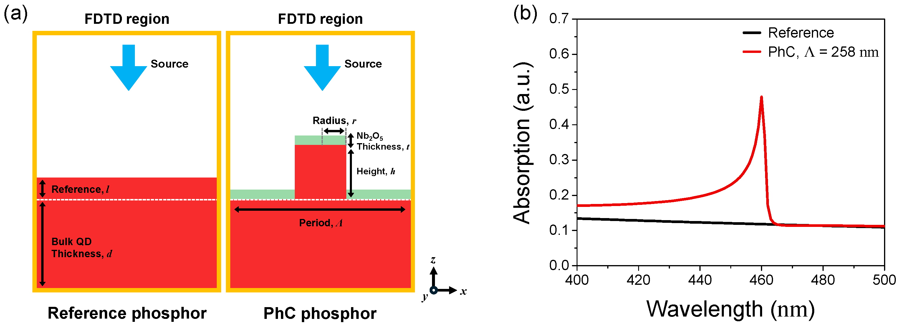
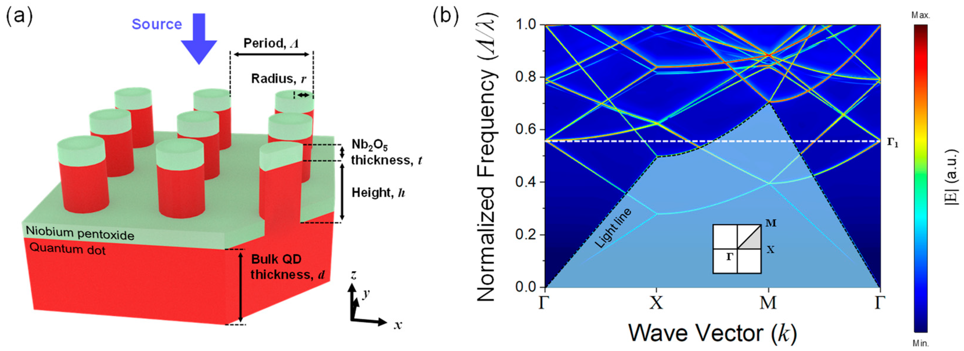
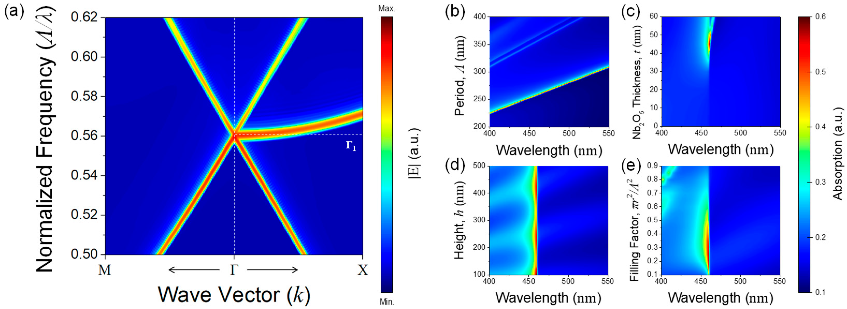
2. Design of a 2D PhC Phosphor Structure

A PhC phosphor with a 1D slab waveguide may have a limited absorption efficiency depending on the polarization state of the excitation light [27]. In this study, we employed a square-lattice-based 2D PhC phosphor model with rotational symmetry, making it independent of the polarization of the incident light. The proposed PhC phosphor model features a high-refractive-index dielectric thin film with a thickness of approximately several tens of nanometers, which is deposited on the surface of a phosphor film patterned with a 2D PhC structure. Figure 1a shows a schematic of the 2D PhC phosphor structure (the period in the PhC is denoted as Λ, the radius of the cylinder as r, the height of the cylinder as h, and the thickness of the high-refractive-index thin film as t). The phosphor materials were considered to be a quantum dot (QD)/polymer composite matrix that can be easily fabricated with a thickness of several micrometers. In the calculations, the refractive index of the phosphor was assumed to be 1.8, while the extinction coefficient was assumed to be 10−3 [53,54]. The high-refractive-index dielectric layer serves as a leaky waveguide to facilitate coupling between excitation photons and the PBE resonance mode. Materials with a high index contrast relative to the phosphor (Δn > 0.5), such as titanium dioxide (TiO2) or niobium pentoxide (Nb2O5), can be considered as candidates for the high-refractive-index layer. In this study, we applied Nb2O5 with a refractive index of approximately 2.37 and excellent heat resistance and durability [55], making it suitable for use in displays and light-emitting devices, to the dielectric thin film. The refractive index and extinction coefficient of the materials used in the calculations were assumed to be constant across the visible wavelength range.
We employed the FDTD method to analyze the photonic band structure of the 2D PhC phosphor model and calculated the electric field profile and absorption efficiency at the PBE resonance wavelength. We calculated the photonic band structure by randomly placing multiple dipole sources within the unit cell and integrating the intensity of the collected electric field. In contrast, to investigate the electric field profile and absorption efficiency within the PhC phosphor structure, we assumed excitation light incident perpendicularly on the surface of the phosphor film. To create an infinitely repeating unit cell in two dimensions, periodic boundary conditions were set along the x and y axes. The unit cell size of the 2D PhC was set as equal to one period (Λ) of the structure, and the minimum mesh size for the simulation was set to 5 nm to ensure the accurate resolution of the photonic crystal structure. The thickness of the bulk QD layer, excluding the PhC-patterned region, was assumed to be 5 µm. The simulation was conducted over a total time of 1000 femtoseconds to ensure a comprehensive analysis of the resonance behavior of the PhC structure. All numerical analyses were conducted using the commercial software Lumerical FDTD.
Figure 1b shows the photonic band structure of the 2D PhC phosphor model. The light line for the nondispersive medium vacuum is indicated by a black dot line, while the direction of the wave vector is shown in the inset. Since the excitation light is incident perpendicularly on the PhC phosphor, it is favorable for inducing the Γ-point PBE resonance mode with a lateral k-vector component of 0, leading to the most efficient absorption [27]. To avoid the emission resonance of the down-conversion phosphor occurring in the wavelength range longer than that of the excitation light, we designed the structure so that the excitation resonance appears at the first PBE mode of the Γ-point (Γ1, white dotted line). Furthermore, to utilize the blue excitation source primarily used in the lighting and display industry, the PhC phosphor model was designed so that the Γ1 PBE wavelength overlaps with the blue-light wavelength (λex ≈ 450~460 nm).

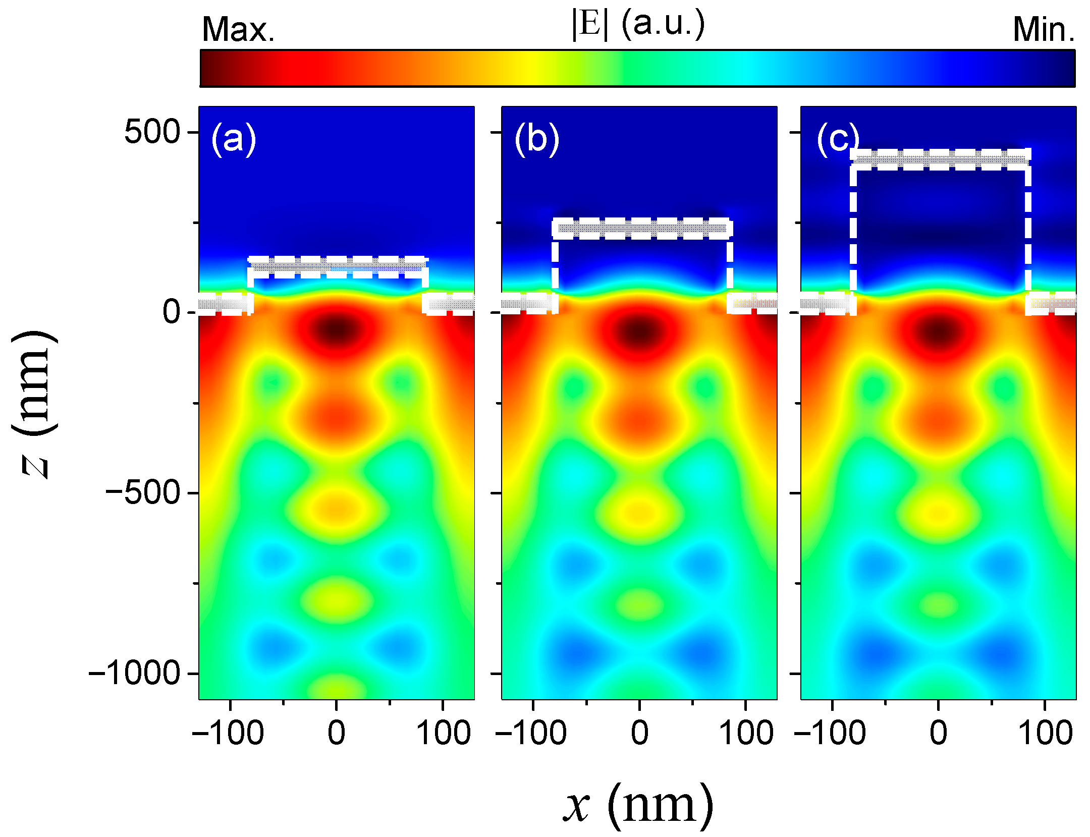
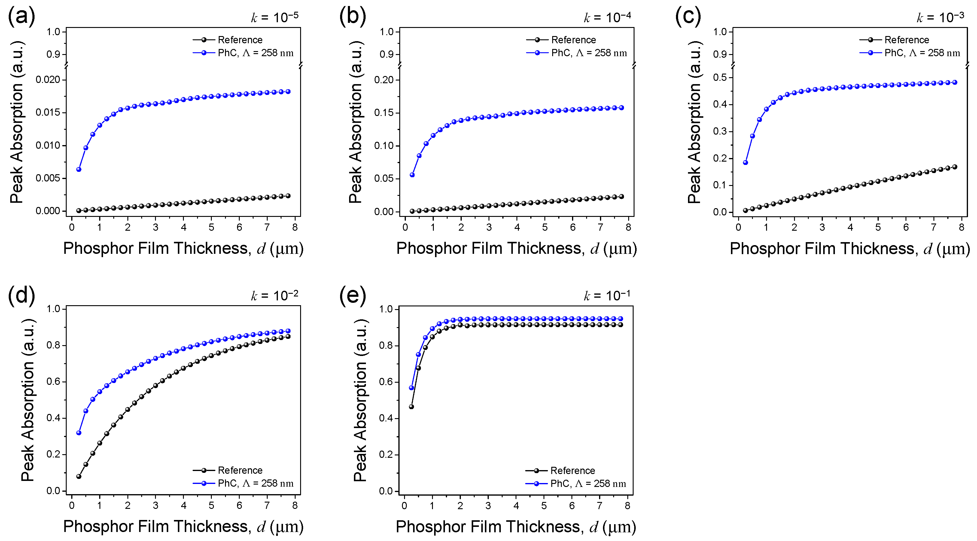
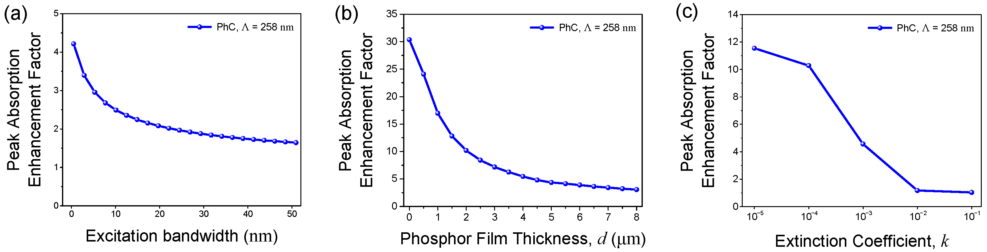
3. Results and Discussion

Figure 2a shows an enlarged view of the photonic band structure of the 2D PhC phosphor model, where an electric field with a high intensity is observed in the X-point direction at Γ1 (Λ/λ~0.56). The excitation photon corresponding to Γ1 is expected to have a very low group velocity (dω/dk~0) inside the PhC phosphor, which leads to a stronger interaction between the light and medium, and thereby enhances the absorption. We calculated the optical power absorbed per unit volume to estimate the light absorption efficiency of the PhC phosphor model. The absorption rate per unit volume is calculated by the divergence of the Poynting vector [56]:
P abs = 0.5   real   · S = 0.5   real   i ω E · D = 0.5   ω   | E | 2   imag ε ,
where ω denotes the angular frequency of the light and ε denotes the medium’s permittivity. Based on this, the light absorption by the phosphor is calculated by integrating Pabs over the spatial domain.
Absorption = phosphor 0.5   ω   | E | 2   imag ε   d V .
The investigation of the absorption efficiency of the PhC phosphor due to the PBE resonance effect allows for designing the most efficient model by adjusting key structural parameters. As indicated in Figure 1a, we analyzed the absorption of a vertically incident light by adjusting the period (Λ) of the PhC phosphor structure, thickness (t) of the Nb2O5 thin film, height (h) of the cylinder, and filling factor (πr2/Λ2) representing the volume ratio of the cylinder within the unit cell. Figure 2b shows the calculated results for the absorption of the 2D PhC phosphor as a function of the period, with high resonance absorption observed at the Γ1 PBE wavelength. It is clear that the PBE resonance wavelength is proportional to the period of the PhC phosphor structure. As shown in the absorption spectra of Nb2O5 thin films with varying thicknesses (Figure 2c), the light cannot be guided on the surface when the Nb2O5 thin film is absent or too thin, and thus the resonance phenomenon cannot be induced. The highest resonance absorption was observed when the thickness of the Nb2O5 thin film increased to approximately 45 nm, while the resonance absorption effect weakened when the thickness exceeded 50 nm. Although a waveguide with a sufficient thickness exceeding half the wavelength would typically be more favorable for light localization, it is worth noting that intentionally forming a thinner film allows the electric field of the resonance mode to overlap with the phosphor region. This suggests that the thickness of the Nb2O5 thin film is an important parameter for optimization of the external quantum yield of the PhC phosphor structure. Furthermore, as the thickness of the Nb2O5 thin film increased, the PBE wavelength exhibited a red shift. This is believed to be due to the increase in the overall effective refractive index of the PhC structure.
Meanwhile, the absorption intensity at the PBE resonance mode exhibited periodic modulation depending on the height of the cylinder, while the resonance wavelength remained unchanged (Figure 2d). To further investigate this behavior, we analyzed the electric field profile at different cylinder heights (100 nm, 240 nm, and 420 nm), as shown in Figure A1. The results indicate that the PBE resonance mode remains strongly localized in the phosphor region along the periodic PhC structure, regardless of the cylinder height. Practically, variations in the height of the phosphor cylinder can influence the effective refractive index of the slab waveguide. However, changes in cylinder height result in subtle variations in absorption intensity rather than spectral shifts. This is likely due to the dominant optical response of the PBE resonance mode at the base of the cylinder and the lower region of the slab waveguide. The cylinder height in the PhC phosphor structure can be appropriately selected by considering both the fabrication conditions and simulation results for the PhC structure. Similarly, as shown in Figure 2e, the filling factor of the PhC structure was an important factor affecting the intensity of resonance absorption. When the proportion of the phosphor cylinder within the unit cell was too large, absorption efficiency significantly decreased. However, when the filling factor was around 30%, a high absorption intensity was observed across a relatively broad wavelength range around the resonance wavelength. This suggests that optimizing the filling factor can not only enhance excitation light absorption but also enable a wider selection of excitation wavelengths. Based on the simulation results (Figure 2b–e), we selected the key parameters for the 2D PhC phosphor to design an optimized structure anticipated to achieve high absorption in the Γ1 PBE mode. Specifically, the PhC phosphor with a 258 nm period, a cylinder height of 100 nm, an Nb2O5 thin-film thickness of 45 nm, and a filling factor of 30% is expected to exhibit the highest absorption of blue excitation light (λex~460 nm).
We calculated the electric field distribution observed in the Γ1 PBE resonance mode of the PhC phosphor. Figure 3a shows the simulated electric field profile in the xz cross section passing through the center of the phosphor cylinder. The electric field for each xy cross section according to the height from the PhC phosphor surface is shown in Figure 3b–d. To conduct a detailed analysis of the electric field distribution formed around the waveguide, the xy cross-sectional electric field was observed at the center of the phosphor cylinder (Figure 3b), in the lower Nb2O5 thin film (Figure 3c), and in the phosphor film under the slab waveguide (Figure 3d). The coordinate system of the structure is shown in the schematic of Figure 1a. As shown in Figure 3a, the light with the Γ1 PBE resonance wavelength is strongly localized in the phosphor region along the periodic PhC structure. We aimed to enhance the excitation light absorption efficiency by adjusting the thickness of the Nb2O5 thin film to overlap the electric field of the resonance mode with the phosphor region. As a result, a relatively weak electric field is observed at the center of the phosphor cylinder (Figure 3b). In contrast, the excitation photons were strongly concentrated around the lower Nb2O5 thin film (Figure 3c), and a strong electric field of the resonance mode was observed across a broad area of the phosphor as intended (Figure 3d). As shown in the simulated absorption spectra, the PhC-patterned structure with a thin slab layer on the surface enables effective overlap of the excitation light with the phosphor due to the leaky waveguide mode. The Nb2O5 layer is designed to be relatively thinner than conventional waveguide thickness (corresponding to half the wavelength of light), allowing the waveguide mode to extend into a larger portion of the phosphor region rather than being strictly confined within the waveguide. This leaky mode expands the interaction volume between the excitation light and the phosphor material, thereby enabling more enhanced light absorption.
To evaluate the enhanced light absorption due to the PBE effect, the absorption enhancement factor of the PhC phosphor was estimated based on the excitation wavelength. The absorption enhancement factor was calculated by dividing the absorption rate of the PhC phosphor film by that of a flat reference phosphor film with the same amount of optically active agents. The structural differences between the reference phosphor region and the 2D PhC phosphor are illustrated in Figure A2a. The thickness of the reference phosphor region was assumed to be the same as the volume occupied by the PhC phosphor structure in the unit cell. At this time, the bulk phosphor thickness (d) is assumed to be the same in both cases. Specifically, the thickness of the flat reference phosphor layer (l) is calculated as the product of the phosphor cylinder height (h) and the volume ratio, which is represented by the filling factor (πr2/Λ2). First, we compared the absorption spectra of PhC phosphor films with different periods. For PhC phosphors with periods of 258, 286, and 314 nm, the optimal excitation wavelengths are 460, 510, and 560 nm, respectively (Figure 3e). For example, exciting the PhC phosphor with a period of 258 nm using a monochromatic blue-light source at 460 nm (red solid line) is expected to increase the absorption efficiency by more than 4.2 times compared to that of a flat reference phosphor. As shown in Figure A2b, the absorption spectra clearly demonstrate the enhancement in absorption efficiency at the PBE resonance wavelength for the 2D PhC phosphor compared to the reference phosphor. Excitation light sources widely used in the lighting and display industry, such as light-emitting diodes (LEDs), typically have a broad spectral bandwidth. Therefore, we also assumed an excitation light source with a Gaussian profile and a full width at half maximum (FWHM) of approximately 30 nm in our simulation. To achieve this, we revised the conventional absorption calculation formula based on the monochromatic source, adapting it for use with broadband sources. Specifically, the absorption spectrum of the broadband source was calculated by integrating the product of the absorption of the monochromatic source and the Gaussian function over the wavelength range [54]:
A b s b r o a d λ p e a k = λ p e a k 3 σ λ p e a k + 3 σ A b s m o n o ( λ ) · 1 2 π · σ e λ λ p e a k 2 2 σ 2 d λ .
Figure 3f shows the absorption enhancement factor of the PhC phosphor as a function of wavelength when using the broadband source. For PhC phosphors with periods of 258, 286, and 314 nm, the optimal center wavelengths of the excitation sources are 452, 502, and 552 nm, respectively. Exciting the PhC phosphor with a period of 258 nm using a blue LED source with a center wavelength of 452 nm (red solid line) is expected to increase the absorption efficiency by more than 1.8 times compared to that of a flat reference phosphor. The absorption efficiency of the PhC phosphor is decreased to some extent compared to when a monochromatic light source is used, likely because the increase in the source’s bandwidth results in more photons that do not contribute to the PBE resonance mode. Nevertheless, the absorption enhancement of the PhC phosphor was still effective even with a broad-bandwidth source.
The PhC phosphor can be applied to various light-emitting devices, and its absorption enhancement factor may vary depending on the bandwidth of the excitation light source. Figure 4a shows the calculated maximum absorption enhancement factor as a function of the excitation source bandwidth. As the bandwidth of the excitation light source decreases, an effective photonic resonance mode is induced, leading to significantly enhanced light absorption. Furthermore, even when the excitation source bandwidth exceeds 50 nm, an absorption enhancement factor greater than 1.6 is predicted, suggesting that our proposed PhC phosphor model operates effectively across a range of excitation sources.
In the latest research on QDs for high-efficiency color conversion, a minimum thickness of several micrometers has been required to achieve sufficient absorption and emission efficiency of the excitation light [50,51]. Although various PhC phosphor structures have been proposed to efficiently excite the phosphor, a practical limitation has been the low quantum efficiency due to the limited amount of optically active agents in the phosphor film constrained by the waveguide thickness [26,27,28,29,30,31]. In this study, we proposed phosphor structures in which the PhC is patterned on the surface of phosphor films with various thicknesses of approximately several micrometers, inducing a resonance mode over a relatively large area to effectively excite the thicker phosphor films. Figure 4b shows the absorption enhancement factor as a function of the thickness of the phosphor film. If the thickness of the PhC phosphor film in our proposed model is very thin, which is similar to previous studies where the phosphor film acts as a waveguide, the absorption enhancement factor could exceed 30. However, as the phosphor film becomes thicker, the absorption enhancement factor decreases. It is worth noting that our goal is not to maximize the absorption enhancement factor but to develop PhC modeling that can be applied to thick phosphor films. As shown in Figure 3a, the PBE resonance mode is most strongly induced in the phosphor film surrounding the waveguide. Therefore, the thinner the PhC phosphor film, the greater the proportion of the phosphor region where the enhanced electric field of the excitation light is distributed across the entire phosphor area. However, as the thickness of the phosphor film decreases, the path of the excitation light is reduced, and the total amount of light that the medium can absorb significantly decreases. Figure A3 shows the total absorption of excitation light by the PhC phosphor (blue dotted line) and the reference phosphor (black dotted line) as a function of phosphor film thickness. Although the enhancement factor may decrease as the phosphor thickness increases, we found that the PhC phosphor consistently outperforms the reference in terms of the total amount of excitation light absorbed.
Furthermore, in the development of high-efficiency optical devices, the extinction coefficient of phosphor materials is a critical factor in determining quantum efficiency. Phosphors with a low extinction coefficient cannot absorb light sufficiently, resulting in significantly low color-conversion efficiency. PhC phosphors can be an effective alternative to overcome low quantum efficiency [29]. Figure 4c shows the absorption enhancement factor of the PhC phosphor as a function of the phosphor’s extinction coefficient. When the extinction coefficient is very low, around 10−5, excitation light can propagate sufficiently through the PhC region, effectively inducing the PhC resonance mode and enabling high resonance absorption. Conversely, when the extinction coefficient is high, above 10−2, excitation light is absorbed by phosphor molecules before it fully traverses the PhC region, inevitably diminishing the PBE resonance effect. Therefore, the PhC phosphor structure proposed in this study is effective when the extinction coefficient of the phosphor medium is below 10−3. This approach is especially beneficial for applications involving phosphors with a low extinction coefficient or low internal quantum efficiency.

4. Conclusions

We propose an advanced 2D PhC phosphor model that overcomes limitations related to phosphor thickness to enhance the absorption efficiency of phosphor films. Using the FDTD method, we designed a PhC phosphor structure integrated with a high-refractive-index dielectric thin film and analyzed the absorption efficiency of excitation photons. A high-refractive-index dielectric layer with an optimized thickness effectively induced the PBE resonance mode within the phosphor film, significantly enhancing absorption efficiency. The absorption efficiency of the optimized PhC phosphor model is expected to increase by approximately 4.2 times compared to the reference phosphor when using monochromatic sources at the PBE resonance wavelength and by approximately 1.8 times when using broadband sources with a 30 nm bandwidth. The proposed PhC phosphor model can be applied with various thicknesses to optimize the excitation absorption and color-conversion efficiency of light-emitting devices. Our slab waveguide-based 2D PhC phosphor film can be implemented through laser interference lithography and nanoimprinting techniques [52]. In the future, we aim to experimentally validate the effectiveness of the 2D PhC phosphor film by conducting optical measurements based on the theoretical predictions presented in this study. These efforts will help bridge the gap between theoretical modeling and practical applications of PhC phosphor films in advanced light-emitting devices. In addition, the proposed PhC phosphor is not limited to specific materials, but can be applied to a wide range of optoelectronic applications.

Author Contributions

K.M. conceived the idea of the paper. T.K. performed the numerical calculations. All authors contributed to the analysis of the results and wrote the manuscript. All authors have read and agreed to the published version of the manuscript.

Funding

This research was supported by a National Research Foundation of Korea grant funded by the Ministry of Science and ICT (No. 2021R1C1C1007405), and the Korea Environmental Industry & Technology Institute (KEITI) funded by the Ministry of Environment (MOE) (Training DX-based carbon supply network environmental experts).

Institutional Review Board Statement

Not applicable.

Informed Consent Statement

Not applicable.

Data Availability Statement

The data that support the presented results are available from the corresponding author upon reasonable request.

Conflicts of Interest

The authors declare no conflicts of interest.

Appendix A

Figure A1. Electric field profile in the Γ1 PBE resonance mode when the height (h) of the phosphor cylinder is (a) 100 nm, (b) 240 nm, and (c) 420 nm, respectively.
Photonics 12 00010 g0a1
Figure A2. (a) Schematic diagram of the structural differences between the flat reference phosphor and PhC phosphor. (b) Comparison of absorption spectra between the reference and PhC phosphor.
Photonics 12 00010 g0a2
Figure A3. Comparison of absorption efficiencies as a function of the phosphor film thickness according to the extinction coefficient (k). The peak absorption enhancement factor was found for an extinction coefficient k of (a) 10−5, (b) 10−4, (c) 10−3, (d) 10−2, and (e) 10−1.
Photonics 12 00010 g0a3

References

  1. Kumar, M.; Kumar, A.; Makki, A.H.; Seong, K.-S.; Park, S.-H. Quantum dot scaffold phosphors: Maximizing luminescence quantum yield via different stock environments. Mater. Lett. 2020, 259, 126846. [Google Scholar] [CrossRef]
  2. Chávez, D.; Garcia, C.R.; Oliva, J.; Diaz-Torres, L.A. A review of phosphorescent and fluorescent phosphors for fingerprint detection. Ceram. Int. 2021, 47, 10–41. [Google Scholar] [CrossRef]
  3. Hariyani, S.; Sójka, M.; Setlur, A.; Brgoch, J. A guide to comprehensive phosphor discovery for solid-state lighting. Nat. Rev. Mater. 2023, 8, 759–775. [Google Scholar] [CrossRef]
  4. Ryu, J.-E.; Park, S.; Park, Y.; Ryu, S.-W.; Hwang, K.; Jang, H.W. Technological breakthroughs in chip fabrication, transfer, and color conversion for high-performance micro-LED displays. Adv. Mater. 2023, 35, 2204947. [Google Scholar] [CrossRef] [PubMed]
  5. Kim, H.; Lee, S.; Shin, J.; Zhu, M.; Akl, M.; Lu, K.; Han, N.M.; Baek, Y.; Cang, C.S.; Suh, J.M.; et al. Graphene nanopattern as a universal epitaxy platform for single-crystal membrane production and defect reduction. Nat. Nanotechnol. 2022, 17, 1054–1059. [Google Scholar] [CrossRef]
  6. Meng, Y.; Feng, J.; Han, S.; Xu, Z.; Mao, W.; Zhang, T.; Kim, J.S.; Roh, I.; Zhao, Y.; Kim, D.-H.; et al. Photonic van der Waals integration from 2D materials to 3D nanomembranes. Nat. Rev. Mater. 2023, 8, 498–517. [Google Scholar] [CrossRef]
  7. Nair, G.B.; Swart, H.C.; Dhoble, S.J. A review on the advancements in phosphor-converted light emitting diodes (pc-LEDs): Phosphor synthesis, device fabrication and characterization. Prog. Mater. Sci. 2020, 109, 100622. [Google Scholar] [CrossRef]
  8. Huang, Y.-M.; Singh, K.J.; Liu, A.-C.; Lin, C.-C.; Chen, Z.; Wang, K.; Lin, Y.; Liu, Z.; Wu, T.; Kuo, H.C. Advances in quantum-dot-based displays. Nanomaterials 2020, 10, 1327. [Google Scholar] [CrossRef]
  9. Liu, Z.; Lin, C.-H.; Hyun, B.-R.; Sher, C.-W.; Lv, Z.; Luo, B.; Jiang, F.; Wu, T.; Ho, C.-H.; Kuo, H.-C.; et al. Micro-light-emitting diodes with quantum dots in display technology. Light Sci. Appl. 2020, 9, 83. [Google Scholar] [CrossRef]
  10. Charak, I.; Manhas, M.; Bedyal, A.K.; Singh, S.; Srivastava, A.; Swart, H.C.; Kumar, V. Structural and spectral studies of highly pure red-emitting Ca3B2O6: Eu3+ phosphors for white light emitting diodes. J. Alloys Compd. 2021, 869, 159363. [Google Scholar] [CrossRef]
  11. Panigrahi, K.; Nag, A. Challenges and strategies to design phosphors for future white light emitting diodes. J. Phys. Chem. C 2022, 126, 8553–8564. [Google Scholar] [CrossRef]
  12. Wang, Y.; Wang, Z.; Wei, G.; Yang, Y.; He, S.; Li, J.; Shi, Y.; Li, R.; Zhang, J.; Li, P. Highly efficient and stable near-infrared broadband garnet phosphor for multifunctional phosphor-converted light-emitting diodes. Adv. Opt. Mater. 2022, 10, 2200415. [Google Scholar] [CrossRef]
  13. Jiang, H.; Chen, L.; Zheng, G.; Luo, Z.; Wu, X.; Liu, Z.; Li, R.; Liu, Y.; Sun, P.; Jiang, J. Ultra-efficient GAGG: Cr3+ ceramic phosphor-converted laser diode: A promising high-power compact near-infrared light source enabling clear imaging. Adv. Opt. Mater. 2022, 10, 2102741. [Google Scholar] [CrossRef]
  14. Jang, E.; Jang, H. Review: Quantum dot light-emitting diodes. Chem. Rev. 2023, 123, 4663–4692. [Google Scholar] [CrossRef]
  15. Song, K.-H.; Peng, M.; Wang, J.-J.; Feng, L.-Z.; Yin, Y.-C.; Song, Y.-H.; Ru, X.-C.; Xie, Y.-P.; Zhang, G.; Deng, Z.; et al. Copper-Iodide Hybrid Clusters with Partial Distortion Enable High-Performance Full-Visible-Spectrum White-Light-Emitting Diodes. J. Am. Chem. Soc. 2024, 146, 34199–34208. [Google Scholar] [CrossRef]
  16. Zhao, K.; Ma, Z.; Yin, L.; Hui, B.; Si, H.; Tong, X.; Tang, H.; Cao, P.; Huang, S. Site preference and defect engineering of a highly efficient blue-emitting phosphor Sr2SiO4:Ce3+/K+ toward thermally enhanced luminescence. Inorg. Chem. Front. 2023, 10, 2314–2324. [Google Scholar] [CrossRef]
  17. Wang, S.; Xu, Y.; Chen, T.; Jiang, W.; Liu, J.; Zhang, X.; Jiang, W.; Wang, L. A red phosphor LaSc3(BO3)4:Eu3+ with zero-thermal-quenching and high quantum efficiency for LEDs. Chem. Eng. J. 2021, 404, 125912. [Google Scholar] [CrossRef]
  18. Oliver, R.D.J.; Caprioglio, P.; Peña-Camargo, F.; Buizza, L.R.V.; Zu, F.; Ramadan, A.J.; Motti, S.G.; Mahesh, S.; McCarthy, M.M.; Warby, J.H.; et al. Understanding and suppressing non-radiative losses in methylammonium-free wide-bandgap perovskite solar cells. Energy Environ. Sci. 2022, 15, 714–726. [Google Scholar] [CrossRef]
  19. Chen, M.; Lu, L.; Yu, H.; Li, C.; Zhao, N. Integration of colloidal quantum dots with photonic structures for optoelectronic and optical devices. Adv. Sci. 2021, 8, 2101560. [Google Scholar] [CrossRef] [PubMed]
  20. Lee, S.; Kim, C.U.; Bae, S.; Liu, Y.; Noh, Y.I.; Zhou, Z.; Leu, P.W.; Choi, K.J.; Lee, J.-K. Improving light absorption in a perovskite/Si tandem solar cell via light scattering and UV-down shifting by a mixture of SiO2 nanoparticles and phosphors. Adv. Funct. Mater. 2022, 32, 2204328. [Google Scholar] [CrossRef]
  21. Yang, X.; Shui, F.; Yu, Y.; Yi, Z.; Li, H.; Xu, Z.; Zhang, F.; Xiong, J.; Liu, X.; Wangyang, P.; et al. All layers patterned conical nanostructured thin-film silicon solar cells for light-trapping efficiency improvement. Opt. Express 2023, 31, 42111–42124. [Google Scholar] [CrossRef]
  22. Gaurav, A.; Chen, C.-S.; Tsai, C.-Y.; Ye, Z.-T.; Lin, C.-F. Stable colour conversion layer with enhanced conversion efficiency by incorporating nanoparticles for micro-LED display application. Mater. Today Chem. 2024, 39, 102184. [Google Scholar] [CrossRef]
  23. Hyun, B.-R.; Sher, C.-W.; Chang, Y.-W.; Lin, Y.; Liu, Z.; Kuo, H.-C. Dual role of quantum dots as color conversion layer and suppression of input light for full-color micro-LED displays. J. Phys. Chem. Lett. 2021, 12, 6946–6954. [Google Scholar] [CrossRef]
  24. Park, H.; Hahm, D.; Cho, H.; Shin, J.-W.; Kang, C.-M.; Ahn, D.-H.; Joo, C.-W.; Kwon, B.-H.; Kim, K.; Kim, J.Y.; et al. Efficient quantum dot color conversion layer with mixed spherical/rod-shaped scattering particles. ACS Appl. Opt. Mater. 2023, 1, 289–297. [Google Scholar] [CrossRef]
  25. Lee, T.-Y.; Miao, W.-C.; Hung, Y.-Y.; Bai, Y.-H.; Chen, P.-T.; Huang, W.-T.; Chen, K.-A.; Lin, C.-C.; Chen, F.-C.; Hong, Y.-H.; et al. Ameliorating uniformity and color conversion efficiency in quantum dot-based micro-LED displays through blue–UV hybrid structures. Nanomaterials 2023, 13, 2099. [Google Scholar] [CrossRef] [PubMed]
  26. Min, K.; Choi, S.; Choi, Y.; Jeon, H. Enhanced fluorescence from CdSe/ZnS quantum dot nanophosphors embedded in a one-dimensional photonic crystal backbone structure. Nanoscale 2014, 6, 14531–14537. [Google Scholar] [CrossRef] [PubMed]
  27. Min, K.; Jung, H.; Park, Y.; Cho, K.-S.; Roh, Y.-G.; Hwang, S.W.; Jeon, H. A colloidal quantum dot photonic crystal phosphor: Nanostructural engineering of the phosphor for enhanced color conversion. Nanoscale 2017, 9, 8703–8709. [Google Scholar] [CrossRef] [PubMed]
  28. Lee, J.; Min, K.; Park, Y.; Cho, K.-S.; Jeon, H. Photonic crystal phosphors integrated on a blue LED chip for efficient white light generation. Adv. Mater. 2018, 30, 1703506. [Google Scholar] [CrossRef]
  29. Mao, C.; Min, K.; Bae, K.; Cho, S.; Xu, T.; Jeon, H.; Park, W. Enhanced upconversion luminescence by two-dimensional photonic crystal structure. ACS Photonics 2019, 6, 1882–1888. [Google Scholar] [CrossRef]
  30. Lee, T.-Y.; Lee, J.; Park, Y.; Cho, K.-S.; Min, K.; Jeon, H. 2D square lattice photonic crystal phosphor films for efficient and excitation polarization insensitive color conversion. Adv. Opt. Mater. 2019, 7, 1900209. [Google Scholar] [CrossRef]
  31. Lee, H.; Lee, T.-Y.; Park, Y.; Cho, K.-S.; Rho, Y.-G.; Choo, H.; Jeon, H. Structurally engineered colloidal quantum dot phosphor using TiO2 photonic crystal backbone. Light Sci. Appl. 2022, 11, 318. [Google Scholar] [CrossRef]
  32. Lee, T.-Y.; Park, Y.; Jeon, H. Resonant cavity phosphor. Nat. Commun. 2023, 14, 6661. [Google Scholar] [CrossRef] [PubMed]
  33. Kim, T.; Lee, J.; Hwang, J.; Kim, D.; Hwang, K.; Min, K. Highly efficient color conversion of 3D photonic crystal phosphor films for micro-light-emitting diode applications. Adv. Photonics Res. 2024, 5, 2300297. [Google Scholar] [CrossRef]
  34. Yablonovitch, E. Inhibited spontaneous emission in solid-state physics and electronics. Phys. Rev. Lett. 1987, 58, 2059–2062. [Google Scholar] [CrossRef] [PubMed]
  35. John, S.; Quang, T. Spontaneous emission near the edge of a photonic band gap. Phys. Rev. A 1994, 50, 1764–1769. [Google Scholar] [CrossRef]
  36. Baba, T. Slow light in photonic crystals. Nat. Photonics 2008, 2, 465–473. [Google Scholar] [CrossRef]
  37. Do, Y.R.; Kim, Y.C.; Song, Y.-W.; Cho, C.-O.; Jeon, H.; Lee, Y.-J.; Kim, S.-H.; Lee, Y.-H. Enhanced light extraction from organic light-emitting diodes with 2D SiO2/SiNx photonic crystals. Adv. Mater. 2003, 15, 1214–1218. [Google Scholar] [CrossRef]
  38. Kim, D.-H.; Cho, C.-O.; Roh, Y.-G.; Jeon, H.; Park, Y.S.; Cho, J.; Im, J.S.; Sone, C.; Park, Y.; Choi, W.J.; et al. Enhanced light extraction from GaN-based light-emitting diodes with holographically generated two-dimensional photonic crystal patterns. Appl. Phys. Lett. 2005, 87, 203508. [Google Scholar] [CrossRef]
  39. Wierer Jr, J.J.; David, A.; Megens, M.M. III-nitride photonic-crystal light-emitting diodes with high extraction efficiency. Nat. Photonics 2009, 3, 163–169. [Google Scholar] [CrossRef]
  40. Kim, S.; Lee, J.; Jeon, H.; Kim, H.J. Fiber-coupled surface-emitting photonic crystal band edge laser for biochemical sensor applications. Appl. Phys. Lett. 2009, 94, 133503. [Google Scholar] [CrossRef]
  41. Matioli, E.; Brinkley, S.; Kelchner, K.M.; Hu, Y.-L.; Nakamura, S.; DenBaars, S.; Speck, J.; Weisbuch, C. High-brightness polarized light-emitting diodes. Light Sci. Appl. 2012, 1, e22. [Google Scholar] [CrossRef]
  42. Zhang, Q.; Tavakoli, M.M.; Gu, L.; Zhang, D.; Tang, L.; Gao, Y.; Guo, J.; Lin, Y.; Leung, S.-F.; Poddar, S.; et al. Efficient metal halide perovskite light-emitting diodes with significantly improved light extraction on nanophotonic substrates. Nat. Commun. 2019, 10, 727. [Google Scholar] [CrossRef] [PubMed]
  43. Wu, P.; Wang, J.; Jiang, L. Bio-inspired photonic crystal patterns. Mater. Horiz. 2020, 7, 338–365. [Google Scholar] [CrossRef]
  44. Qian, Z.; Shan, L.; Zhang, X.; Liu, Q.; Ma, Y.; Gong, Q.; Gu, Y. Spontaneous emission in micro-or nanophotonic structures. PhotoniX 2021, 2, 21. [Google Scholar] [CrossRef]
  45. Piper, J.R.; Fan, S. Total absorption in a graphene monolayer in the optical regime by critical coupling with a photonic crystal guided resonance. ACS Photonics 2014, 1, 347–353. [Google Scholar] [CrossRef]
  46. Piper, J.R.; Liu, V.; Fan, S. Total absorption by degenerate critical coupling. Appl. Phys. Lett. 2014, 104, 251110. [Google Scholar] [CrossRef]
  47. Liu, Y.; Chadha, A.; Zhao, D.; Piper, J.R.; Jia, Y.; Shuai, Y.; Menon, L.; Yang, H.; Ma, Z.; Fan, S.; et al. Approaching total absorption at near infrared in a large area monolayer graphene by critical coupling. Appl. Phys. Lett. 2014, 105, 181105. [Google Scholar] [CrossRef]
  48. Qing, Y.M.; Huang, Z.; Jiang, H.; Li, B. Polarization-dependent thermal-tunable graphene-based metamaterial exploiting critical coupling with guided mode resonances. J. Opt. Soc. Am. B 2023, 40, 233–238. [Google Scholar] [CrossRef]
  49. Qing, Y.M.; Ma, H.F.; Cui, T.J. Tailoring anisotropic perfect absorption in monolayer black phosphorus by critical coupling at terahertz frequencies. Opt. Express 2018, 26, 32442–32450. [Google Scholar] [CrossRef]
  50. Hu, Z.; Yin, Y.; Ali, M.U.; Peng, W.; Zhang, S.; Li, D.; Zou, T.; Li, Y.; Jiao, S.; Chen, S.-J.; et al. Inkjet printed uniform quantum dots as color conversion layers for full-color OLED displays. Nanoscale 2020, 12, 2103–2110. [Google Scholar] [CrossRef]
  51. Weng, Y.; Chen, S.; Zhang, Y.; Sun, L.; Wu, Y.; Yan, Q.; Guo, T.; Zhou, X.; Wu, C. Fabrication and color conversion of patterned InP/ZnS quantum dots photoresist film via a laser-assisted route. Opt. Laser Technol. 2021, 140, 107026. [Google Scholar] [CrossRef]
  52. Umar, M.; Min, K.; Jeon, H.; Kim, S. Single-mode distributed feedback laser operation with no dependence on the morphology of the gain medium. Ann. Phys. 2017, 529, 1700034. [Google Scholar] [CrossRef]
  53. Zimmennann, L.; Weibel, M.; Caseri, W.; Suter, U.W. High refractive index films of polymer nanocomposites. J. Mater. Res. 1993, 8, 1742–1748. [Google Scholar] [CrossRef]
  54. Min, K.; Choi, Y.K.; Jeon, H. Model calculations for enhanced fluorescence in photonic crystal phosphor. Opt. Express 2012, 20, 2452–2459. [Google Scholar] [CrossRef] [PubMed]
  55. Abood, M.; Salim, E.T.; Saimon, J.A. Optical investigations of Nb2O5 at different temperatures for optoelectronic devices. J. Ovonic Res. 2019, 15, 109–115. [Google Scholar]
  56. Taflove, A.; Hagness, S.C. Computational Electrodynamics: The Finite-Difference Time-Domain Method, 3rd ed.; Artech House Publishers: Norwood, MA, USA, 2005. [Google Scholar]
Figure 1. (a) Schematic and (b) photonic band structure of the 2D PhC phosphor model.
Photonics 12 00010 g001
Figure 2. (a) Γ1 PBE mode in the photonic band structure of the 2D PhC phosphor structure. Absorption spectra according to the (b) period, (c) Nb2O5 thickness, (d) height, and (e) filling factor.
Photonics 12 00010 g002
Figure 3. Electric field distribution in the Γ1 PBE resonance mode at the (a) xz cross section at the phosphor cylinder center and (bd) xy cross section according to the height from the PhC phosphor surface. Enhancement factor of excitation light absorption using (e) a monochromatic light source and (f) a broadband light source.
Photonics 12 00010 g003
Figure 4. Absorption enhancement factor as a function of the (a) bandwidth of the broadband light source, (b) bulk phosphor film thickness, and (c) extinction coefficient of the phosphor.
Photonics 12 00010 g004
Disclaimer/Publisher’s Note: The statements, opinions and data contained in all publications are solely those of the individual author(s) and contributor(s) and not of MDPI and/or the editor(s). MDPI and/or the editor(s) disclaim responsibility for any injury to people or property resulting from any ideas, methods, instructions or products referred to in the content.

