Abstract
We present a framework to optimize the voltage range of electro-optic polarization controllers (EPC) in polarization-based quantum key distribution (QKD) subsystems. In this study, we consider an EPC capable of modifying both the phase difference between its fast and slow axes and the orientation of the fast axis. This capability allows it to transform any input state of polarization (SOP) into any desired output SOP on the Poincaré sphere using a single wave-plate. When multiple wave-plates are available, properly distributing the required polarization modulation across them effectively reduces the electronic demands, lowers the implementation costs, and enhances the polarization modulation speeds. This optimization is achieved through the application of multi-objective optimization (MOO) and wave-plate splitting techniques. Within a simulation model, using the calibration parameters from a commercially available six-wave-plate EPC, we determined the optimized voltage ranges required to achieve the six, four, and three SOPs typically used in polarization-based QKD protocols. Two voltage reference points are considered in our study: bias voltage points, which result in zero birefringence, and zero voltage points. For optimization procedures centered around the bias voltage points, we observe a significant reduction in the voltage range, from V, for a single wave-plate, to approximately V, for six wave-plates. Furthermore, using wave-plate splitting techniques, we conclude that only two independent wave-plates (four variables) need to be considered in our model to achieve optimized results, which contributes to the efficient design of polarization-based QKD subsystems by minimizing voltage transitions while ensuring precise SOP control, ultimately enabling cost-effective and high-speed polarization modulation.
1. Introduction
As advances in quantum computing pose future risks to an important part of currently employed encryption algorithms [1], quantum key distribution (QKD), together with quantum networks [2], have emerged as a promising solution for secure key distribution. Polarization, one of the different properties of photons that can be used to encode quantum bits in QKD, stands out due to its high versatility in both fiber-optic- [3] and free-space-based links [4], along with its achievable reach [5], key rates [6], and low error rates [7]. This makes it a practical and effective approach compared to other encoding techniques such as time-bin [8,9] and phase encoding [10]. Despite this, polarization-based QKD subsystems still face challenges in their implementation, particularly in enhancing encoding and decoding methods to improve adaptability to external factors, reduce electronic costs, and ensure fast and precise qubit encoding.
In polarization-based discrete variable QKD (DV-QKD), up to six polarization states from three distinct bases can be employed, with four states being the most common, as in protocols like BB84 [11]. Therefore, advancements in polarization control methods that enable fast and precise polarization control are paramount. Several promising polarization control techniques have emerged for controlling polarization in DV-QKD, including balanced Mach–Zehnder interferometers [12] and fiber-based Sagnac loops [13]. The most widely used techniques employ phase modulators [6,14,15], whose key advantage is the potential to achieve encoding/decoding speeds in the tens of GHz range, far exceeding the physical limitations of current single-photon detector (SPD) technology [16,17]. These setups require a well-defined SOP at their input to operate effectively, while also being often limited to the generation of four or fewer SOPs [18].
In this context, EPCs offer a promising set of advantages, as they can independently compensate for external SOP changes at the input due to their ability to perform arbitrary polarization transformations, while maintaining competitive encoding speeds in the tens of MHz range. This benefits both the transmitter and receiver sides, with the receiver side, in particular, reaping the most advantages, as EPCs can be used for both basis selection and compensation of polarization drift in the quantum channel, thereby eliminating the need for additional equipment [7]. Research on the use of EPCs has already been conducted, with much of the work focusing on calibration [19,20,21] and their use for compensating polarization drifts [22]. As for their role as encoders/decoders in polarization-based QKD subsystems, previous studies have suggested implementations and evaluated expected performance [23]. Most prior work relies on the well-known behavior of quarter-wave- and half-wave-plates, with the associated electrical requirements reaching up to V. However, a detailed understanding of the actual physical and electrical limitations, as well as the minimal requirements for effective implementation in a QKD system, have yet to be fully explored.
In this paper, we present a framework to enhance the efficiency of multi-wave-plate EPCs in polarization-based QKD subsystems by reducing the voltage ranges and swings required for transitioning between different SOPs. This work builds upon the abstract submitted to the International Conference on Application of Optics and Photonics (AOP) 2024 [24]. Using the calibration parameters of a particular EPC and a given input polarization state, we develop a comprehensive model of its behavior. The framework integrates multi-objective optimization (MOO) algorithms [25], specifically, the non-dominated sorting genetic algorithm (NSGA-II) [26], while simplifying the optimization process by reducing the number of independent variables through wave-plate splitting. Our results demonstrate that a voltage range of is sufficient for transitioning between all orthogonal SOPs when operations are centered around bias voltage points, while a range of is required when centered around zero volts.
This paper is organized as follows: Section 2 provides an overview of EPCs, detailing their working principles and significance in QKD systems. Section 3 introduces the optimization targets and cost functions aimed at minimizing voltage ranges and swings while ensuring SOP accuracy. It also describes the algorithm implementation, focusing on MOO frameworks such as NSGA-II, and outlines a method for wave-plate splitting. Section 4 presents the simulation results, analyzing the voltage requirements around bias points and around zero volts, as well as the maximum voltage swings for various EPC configurations. Finally, Section 5 concludes the paper by summarizing the findings and discussing their implications.
2. EPC Description
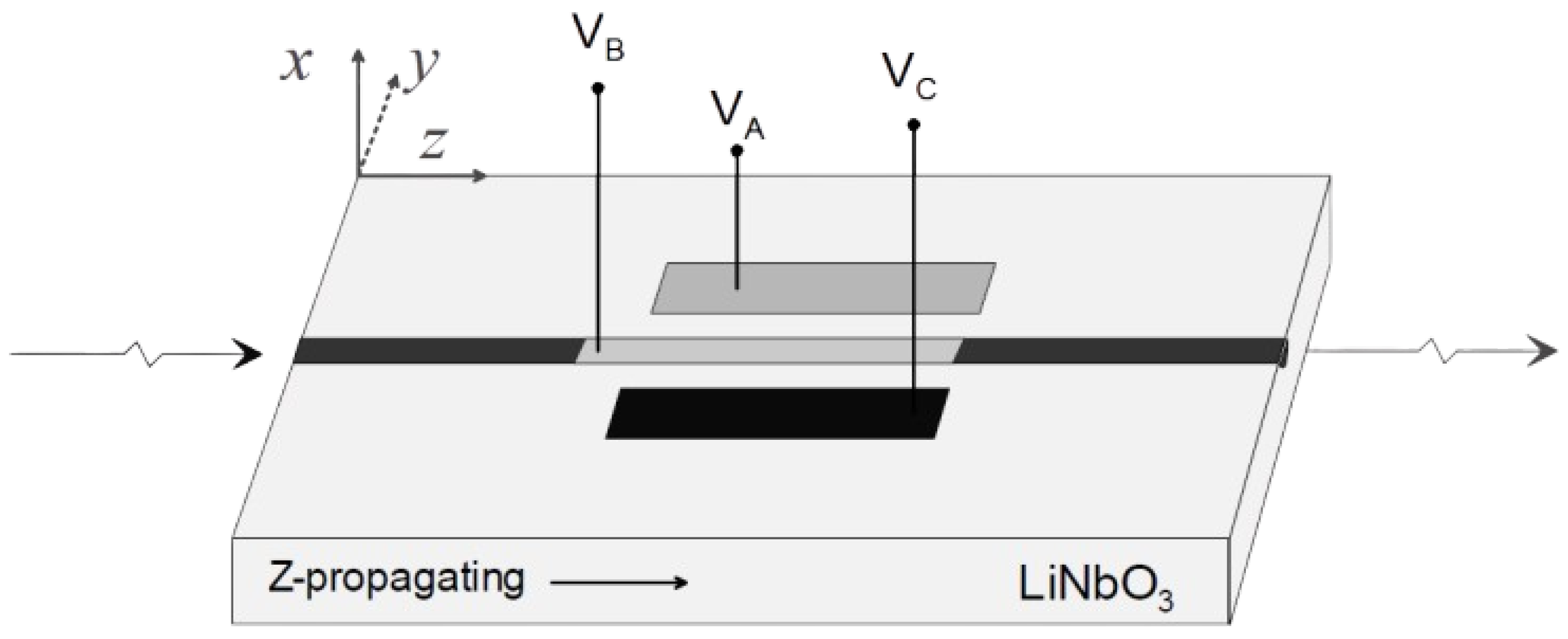
An EPC, in the context of this work, is device capable of achieving an arbitrary output SOP irrelevant to its input SOP. These devices can operate through piezoelectric effects, such as with fiber squeezers [7], or electro-optic, in the case of lithium niobate ()-based EPCs [27]. Most EPCs are composed of multiple wave-plates, because a single wave-plate can typically only modify either the phase difference between the fast and slow axes or the orientation of the fast axis. Among these two, changing the phase difference between the axes is the more common approach. The EPC we based our study on, sourced from EOSPACE, is based on and makes use of the electro-optical effect. is a substrate whose refractive index changes upon the establishment of an electrical potential difference across its terminals [27], in an implementation similar to Figure 1. Unlike other EPCs, one of its key features, in addition to its fast response time (<100 ns), is its ability to simultaneously adjust both the phase difference between its axes and the orientation of the fast axis for each wave-plate.

Figure 1.
Schematic representation of the controller waveguide, x-cut on substrate with a titanium diffused channel waveguide in the z-direction, featuring an independent electrode configuration , from [28].
Wave-plates in an EPC are treated as general linear retarders. Their properties can be described using Mueller calculus [29]. The matrix for a general linear retarder can be written as
where is the phase difference between the fast and slow axis, and is the orientation of the fast axis. To calculate the effect of a cascade of multiple wave-plates on light polarization, such as with an EPC, we multiply each wave-plate matrix (1) in reverse order to the light propagation. This framework is generic and applicable to most commonly found EPCs, regardless of their number of wave-plates. The resulting overall transformation can be expressed as
where and represent the input and output SOP, respectively, as Stokes vectors, whose entries comprise the , , and parameters. The transformation matrix is obtained by concatenating all wave-plate matrices, starting from , the last wave-plate that light exits, to , the first wave-plate in the EPC. From an electrical design standpoint, for the types of the EPCs considered in this work, each wave-plate consists of three electrodes, see Figure 1. Two of these electrodes, and , control the wave-plates’ characteristics, while the third, , is grounded. The relationship between the wave-plate characteristics and the applied voltage can be expressed through the following equations
where , and represents the voltage required to induce a 180-degree phase shift between two orthogonal polarization modes (transverse electric (TE) and transverse magnetic (TM)) within a single wave-plate. is the voltage necessary to transfer all power from one polarization mode (TE) to the other (TM), or vice versa, for a single wave-plate. and correspond to the voltages at which the wave-plates exhibit zero birefringence between the TM and TE modes. The precise values of , , , and should be determined through a calibration process [19,20,21]. However, based on the datasheet provided by EOSPACE [28], we estimate , where N is the total number of EPC wave-plates. Additionally, we assume as an initial approximation.
3. Optimizing Domains of the Wave-Plate Phase Delay and the Fast Axis Orientation
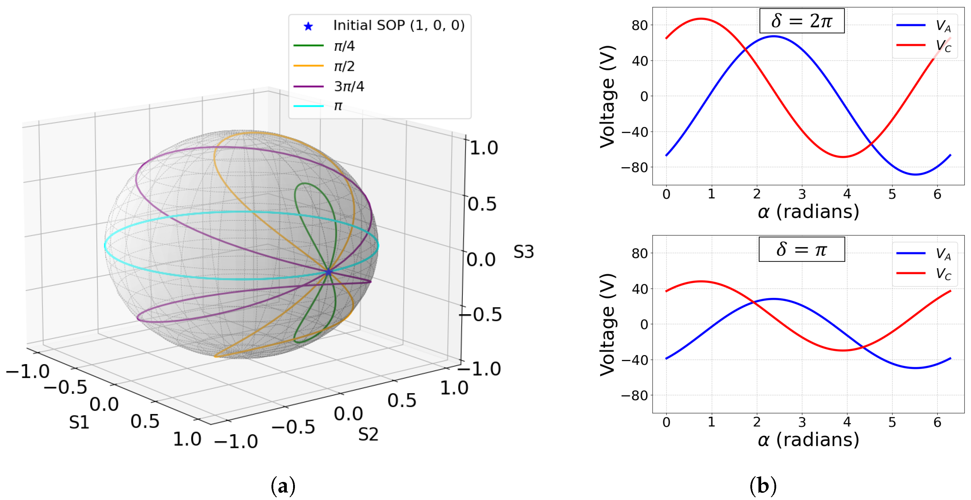
Given that both the phase difference between the fast and slow axes and the orientation of the fast axis can be adjusted, a single wave-plate can act as a complete EPC. In Figure 2a, this behavior is demonstrated, as the entire Poincaré sphere is covered within the domains and . However, this is not the only viable approach. By extending the range of to , the required domain of can be reduced to . The impact of changes in the domain on the corresponding and values is shown in Figure 2b. Higher values result in sinusoidal voltage variations with larger amplitudes, leading to greater differences between SOPs. Since lower voltage amplitudes are more practical for implementation, prioritizing smaller values is preferable.

Figure 2.
(a) Output SOP as a function of wave-plate angle (ranging from 0 to ), considering particular values of phase delay between axis, (). (b) and values in function of with (upper) and (down), for a six-wave-plate EPC model.
Given that our EPC is composed of multiple wave-plates it makes sense to split the polarization changes required to obtain a certain output SOP between them. This distribution reduces the voltage range required for each wave-plate, leading to smaller voltage swings between the target SOPs. Lower voltage swings reduce the electronic power demands and allow for faster response times, potentially enabling higher encoding and decoding frequencies for the polarization-based QKD subsystem. However, the maximum achievable rate is also influenced by other system factors such synchronization constraints, attenuation, polarization drift compensation, and SPD configurations, which together define the overall system performance.
The behavior of each wave-plate is highly non-linear and evolves quickly into a very complex variable space. The Mueller matrix in (1) establishes the relationship between the input and output SOP of a wave-plate, whereas (3) and (5) can be used to obtain the associated voltage values. Due to the potential complexity of the variable space, we develop a framework to optimize the values of and across all wave-plates to both achieve the required SOPs and minimize the voltage ranges needed to accomplish this. Since lower values are expected to result in lower voltage amplitudes, voltage optimization around the bias points corresponding to zero birefringence () is one focus of our study, along with optimization surrounding zero volts.
3.1. Optimization Objectives
The main objectives of the optimization procedure are as follows:
- Minimization of the SOP error in Stokes space.
- Minimization of the absolute maximum voltage deviation from a reference voltage value.
- Minimization of the absolute maximum voltage jump between the SOPs required by a QKD protocol.
The first objective focuses on achieving high output SOP accuracy, which is crucial in QKD implementations. Any uncertainty in polarization control increases the quantum bit error rate (QBER), leading to a reduced secret key rate (SKR) and ultimately limiting the achievable transmission distance [6]. To be able to minimize the error between an SOP associated with an and combination for each wave-plate and the objective SOP, we define as the sum of the differences between the parameters of the Stokes vector, , obtained using the current combination of and and the target Stokes vector, , required in the QKD protocol
where and correspond to each respective Stokes parameter, , , and . The algorithm should also include inequality constraints, rejecting any solutions exceeding a defined threshold. The second optimization objective is the voltage minimization of the absolute maximum voltage deviation from a reference value. Two reference values were considered in this analysis: the bias voltage values representing zero birefringence for each wave-plate and the condition where all wave-plates are set to zero (ground) volts. The bias voltage values are significant because they represent the state where no polarization modulation occurs, while the zero-volt condition reflects a setup in which the wave-plates are centered around the expected average point of an electronic driver, zero. This is accomplished through the use of the following cost function, ,
where and represent the corresponding voltage values from (3) and (5), respectively, associated with the current combination of and for wave-plate i, with m denoting the number of wave-plates intended for use. When minimizing around zero volts, and are set to zero for all i. In contrast, when minimizing around the bias points for each wave-plate, and are set equal to the corresponding values. The deviations are considered in terms of their absolute values, meaning the direction (negative or positive) does not affect the analysis. We only take into account the maximum value, because we want to generalize the implementation and expect all electronic drivers to have equal ranges in all wave-plates. Finally, to address the third optimization objective, i.e., the absolute maximum voltage swing between SOPs, we also make use of (7). This is accomplished, in our implementation, at a later stage, once the first SOPs have been obtained. We set the values of and to the value or the average of values of the wave-plate parameters of previously optimized SOPs. The wave-plate parameters for each new SOP were then obtained sequentially. We only deal with two or three optimization goals simultaneously, which justifies the use of MOO and NSGA-II in particular.
3.2. Algorithm Implementation
To simulate the polarization modulation induced by the EPC, we used (2). The calibration parameters in (3) and (5) were set to , , , and . These specific values were chosen, as they represent the average calibration parameters for our six-wave-plate EPC model sourced from EOSPACE. In this study, we assumed all wave-plates to have equal calibration values. For and , this approach is justified by their low standard deviation (under ) across wave-plates. For and , although the standard variations are slightly larger, ranging between and , they are inconsequential for the optimization procedure centered around the bias voltage points and can be easily compensated in the procedure centered around zero volts by adjusting for wave-plates with values further from zero. This allows for direct performance comparations to the simplified models, discussed in Section 3.3.
NSGA-II was implemented using the Multi-Objective Optimization Python library ‘pymoo’ (version 0.6.1.3) [30], with the seed fixed to one to ensure reproducibility. Inequality constraints were incorporated into the algorithm to ensure that the sum associated with (6) satisfies , corresponding to an angular error of less than 0.29 degrees in the Poincaré sphere. The population size was set to 200 when the current calculation only involved 4 wave-plates or lower, and 400 when it involves a higher number of wave-plates. This approach provided a reasonable trade-off between exploration and computational efficiency while accounting for the increased number of optimization variables as the wave-plate count increases. As a result, the computational time scaled accordingly, with the optimization for 6 wave-plates requiring an average of 171.1 s, while 4 and 2 wave-plate configurations required 94.58 and 38.82 s, respectively, when running on an Intel Core i7-6800K @ 3.4 GHz CPU, 32 GB of RAM, and an Nvidia GeForce GTX 1050 GPU. The constraints in NSGA-II, as well as in ‘pymoo’, were handled using a constraint dominance approach [26].
The absolute maximum voltage deviation was optimized using (7). An inequality constraint was also applied to this equation, through a progressive constraint approach. This dynamic method, chosen to enhance the algorithm’s exploration capabilities, adjusts the constraints based on the solutions found within a given iteration count. In this approach, an initial inequality constraint is set. If the algorithm finds a solution before reaching a maximum pre-defined iteration count, the iteration count resets, and the constraint is reduced by 15%. This procedure is repeated until no valid solution is found. At that point, the algorithm reverts to the last valid constraint and performs all the required iterations to reach a difference between successive iterations below 0.001, for the best voltage range combination. The combination that results in the lowest value for from (7), is selected. Overall, this approach leads to significant improvements in solution quality, providing more consistent results and better convergence compared to a standard minimization approach.
The dependence of the optimization result on the input SOP was also analyzed. Although its state was fixed during a run, its value did affect the final optimization results. Hence, it was considered an object of study, and we present its dependency.
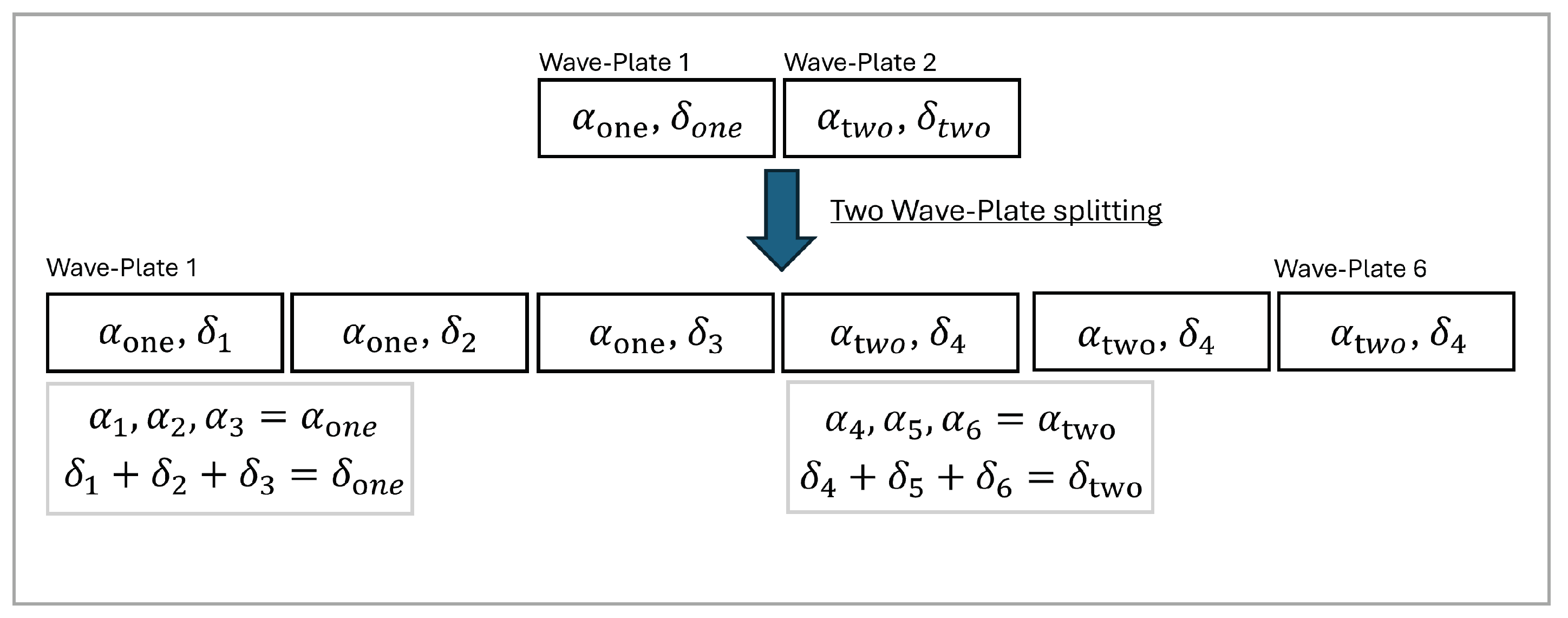
3.3. Wave-Plate Splitting
In Section 3, we demonstrated that a wave-plate capable of modifying both the phase difference between its axes and the orientation of its fast axis can transform any random input SOP into a desired output SOP. We also proposed that distributing the required polarization rotation across multiple wave-plates could significantly improve the system’s efficiency. To illustrate this approach, consider the scenario where achieving a specific output SOP requires a phase difference between the axes of and an orientation of the fast axis of in a single wave-plate configuration. Rather than relying on a single wave-plate, the same output SOP can be achieved using N wave-plates by setting the fast axis orientation of each wave-plate to and distributing the phase difference between the axes across the wave-plates. This is accomplished by ensuring that the sum of all phase differences equals , i.e., . The simplest approach for distributing is to assign for each wave-plate.
Alternatively, we can consider a two wave-plate configuration for transforming the input polarization, which introduces four variables: , , , and . Figure 3 presents a schematic representation of the two wave-plate splitting procedure, where a six wave-plate EPC is divided into two groups. Each group of three wave-plates performs the equivalent function of a single wave-plate in the two wave-plate model.

Figure 3.
Wave-plate splitting process for an EPC. The behavior of a six-wave-plate model is simplified by splitting the variables optimized in a two-wave-plate model; the relative wave-plate order must remain the same.
The procedure must always begin with a model consisting of a lower wave-plate count. Ideally, this count is a divisor of the complete wave-plate EPC model, such as 1, 2, or 3 for a six-wave-plate model. The relative order of the wave-plates must be maintained. The following equations describe the behavior for expanding 1- and 2-wave-plate models, with similar logic extended to higher wave-plate models,
where is the Mueller matrix presented in (1), and and refer to the wave-plates one and two of a simplified model, respectively. The concatenation of matrices is performed in the reverse order of the light propagation, as shown in (2). L and K represent the number of wave-plates used to achieve the same rotation as their corresponding counterparts in the simplified model.
For the simplified wave-plate model to achieve the same maximum voltage deviations as the complete model, it is essential to preserve the proportions , where N is the number of wave-plates in the simplified model, along with the constants and . For instance, in our implementation, we assume , meaning that in a six-wave-plate model, each wave-plate has . Reducing this to an equivalent one-wave-plate model results in being used during the optimization procedure.
4. Simulation Results for Voltage Optimization
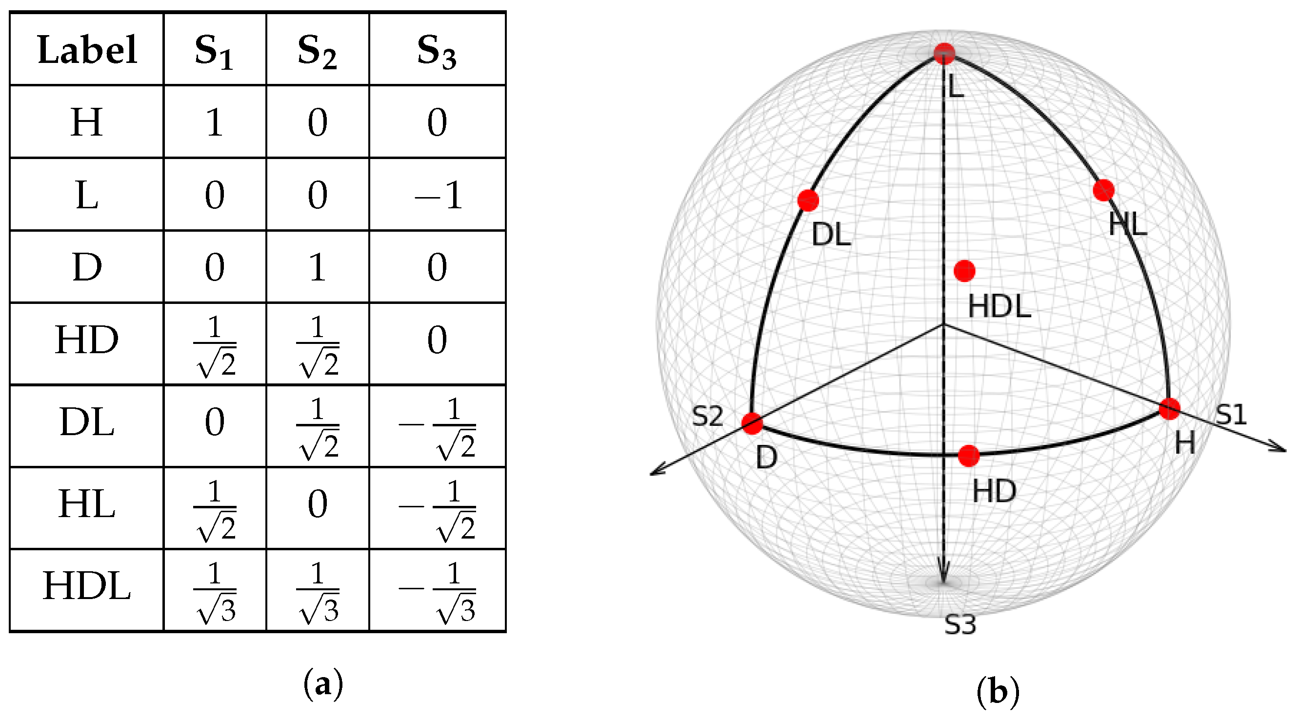
This section presents the simulation results aimed at optimizing the maximum voltage requirements for EPCs employed in polarization-based QKD subsystems. The simulations analyze the absolute maximum voltage deviations and swings required for SOP transitions across various EPC wave-plate configurations, considering both the bias voltage points and zero-volt centering scenarios. Additionally, the results explore the impact of the input SOP and wave-plate splitting on the voltage optimization, highlighting the flexibility and scalability of the proposed framework. In Figure 4, the input polarization labels used throughout the paper are presented.

Figure 4.
(a) Table presenting the SOP labels used throughout the paper alongside the associated Stokes parameter values. (b) Representation of the SOPs listed in Table (a) plotted on the Poincaré sphere.
4.1. Optimization Surrounding Bias Voltage Points
Optimizing the voltage ranges around the bias voltage points, and , of the EPC is highly relevant, since as illustrated in Figure 2, reducing the values leads to smaller voltage ranges. Notably, the bias points correspond to the condition of zero birefringence, where across all wave-plates. In this section, we assume that an implemented electronic driver does not need to account for the bias points, as they can be added as a DC value to its square wave output.
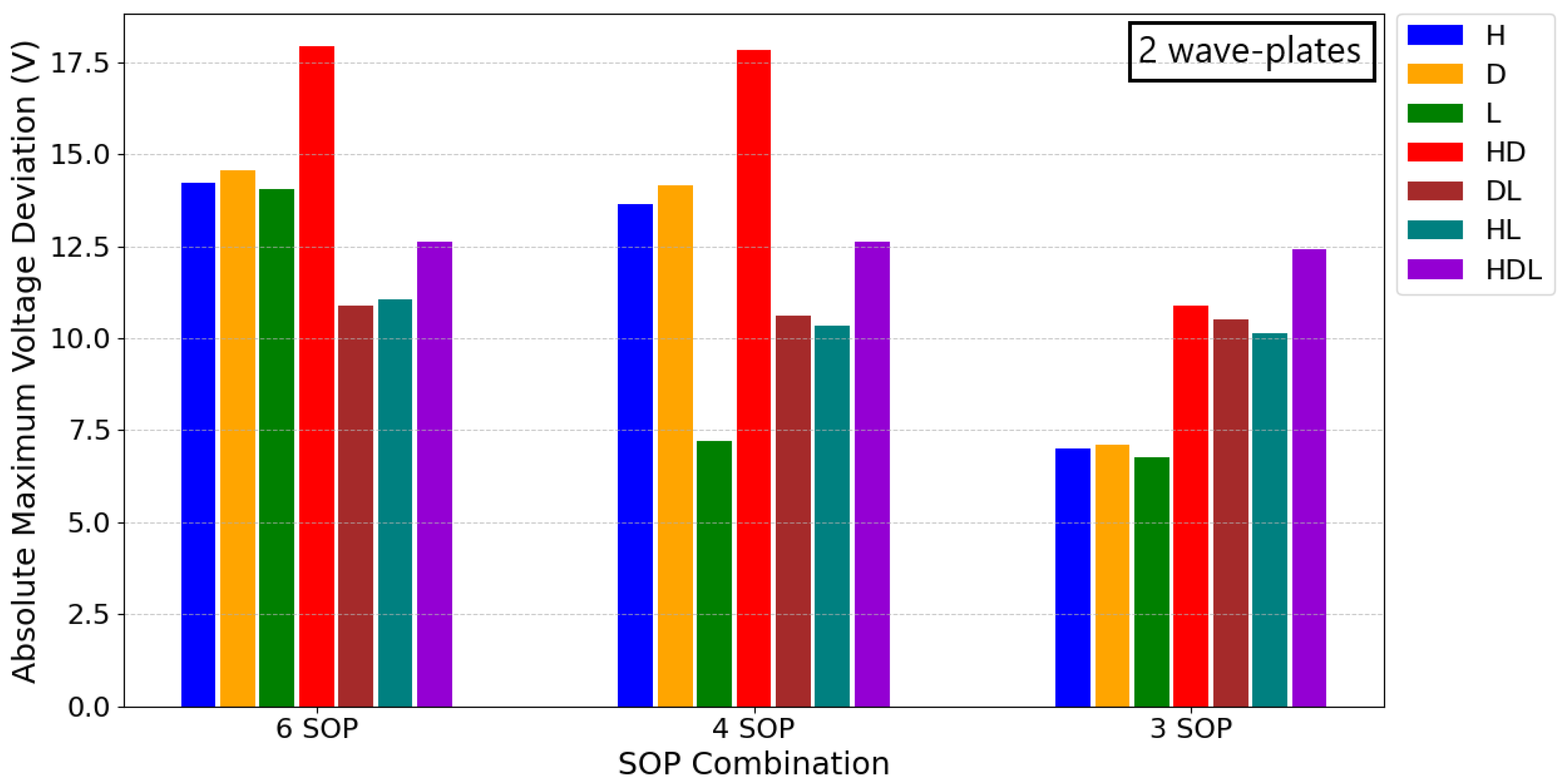
In Figure 5, the influence of each input SOP on the absolute maximum deviation from the bias points is shown, demonstrating its dependence on the combination of SOPs utilized in the QKD protocol. If the input polarization had no significant effect, all bars would exhibit the same magnitude for each of the corresponding SOP combinations; however, this is not observed. Furthermore, the relative magnitude between the SOPs for a given input SOP combination remains consistent regardless of the total number of wave-plates used, except for the single wave-plate scenario; so, the choice to present two wave-plates is not consequential. In Figure 5, the input SOPs such as (DL) and (HL), as well as their opposites on the Poincaré sphere, yield very similar results to each other. Further analysis of other polarization states revealed that for a six SOP implementation, the optimal input polarization would be a state such as (HL) or (DL). For a four SOP setup, starting in one of the SOPs of the circular basis provides the best results, while for a simplified three SOP protocol, beginning within any of the bases yields optimal performance. To ensure the analysis is not limited to specific input SOPs, we focused on the worst-case scenario, from the presented results and additional studies for six SOP and four SOP combinations, where the input SOP is (HD).
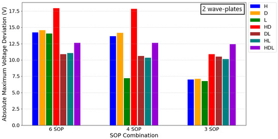
Figure 5.
Bar graph representing the optimized absolute maximum voltage deviation from the bias points for different SOP configurations: six SOP (three bases), four SOP (two bases), and three SOP (two bases excluding one SOP).
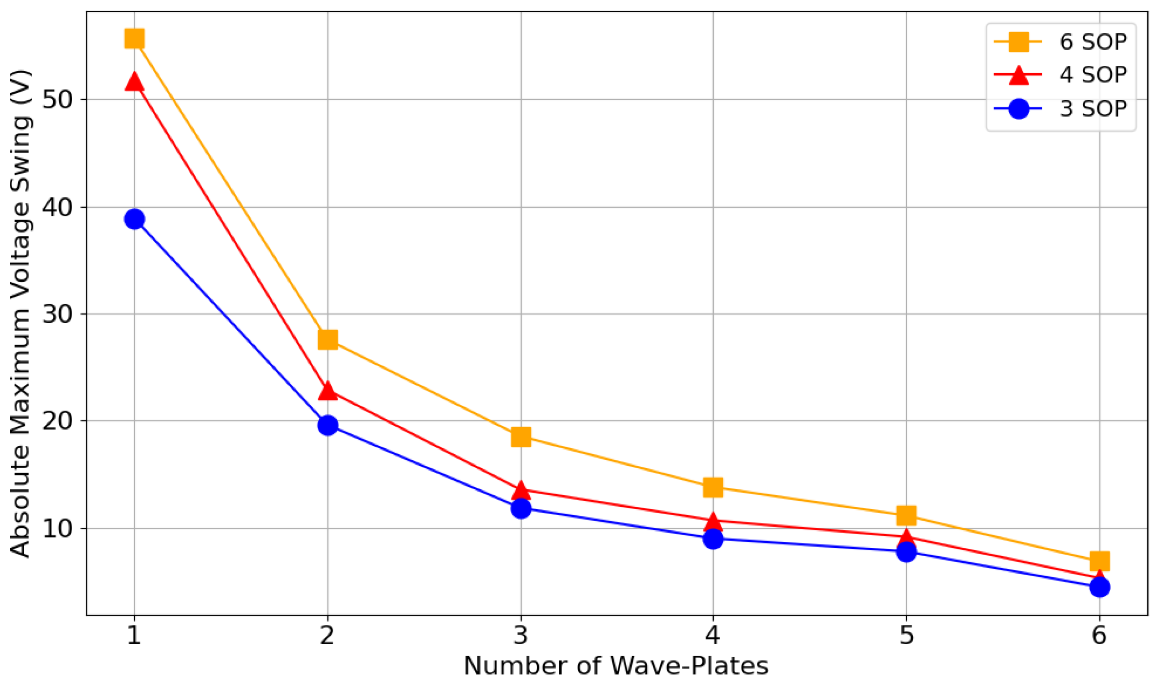
Figure 6 shows the evolution of the absolute maximum voltage deviation from the bias values using the worst input SOP (HD). This is presented as a function of the number of wave-plates in a six-wave-plate EPC model, where unused wave-plates are left at their associated values.

Figure 6.
Absolute maximum voltage deviation from bias, as a function of the number of wave-plates for different SOP combinations (three, four, and six SOP), using a six-wave-plate EPC model, where unused wave-plates are set to their associated values.
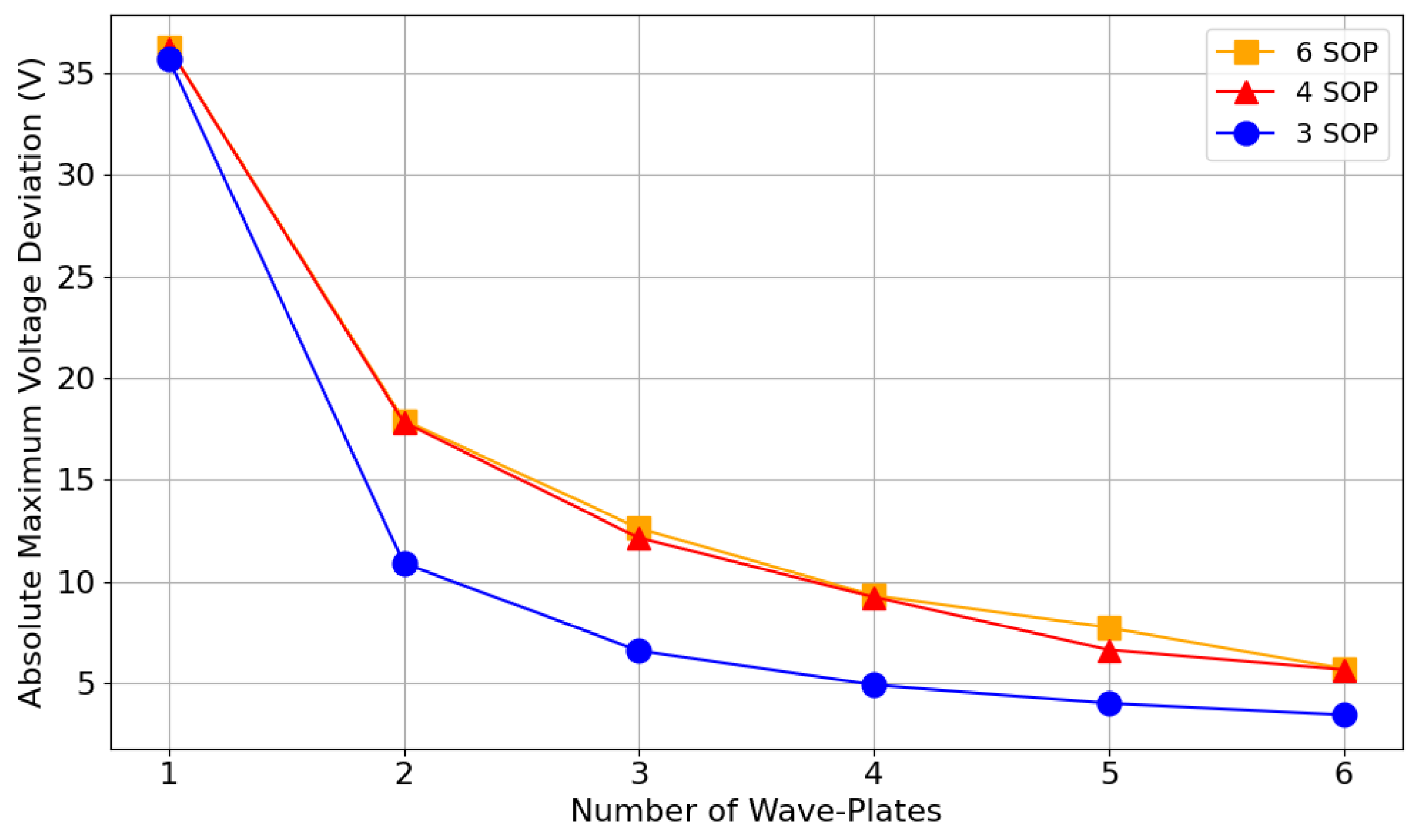
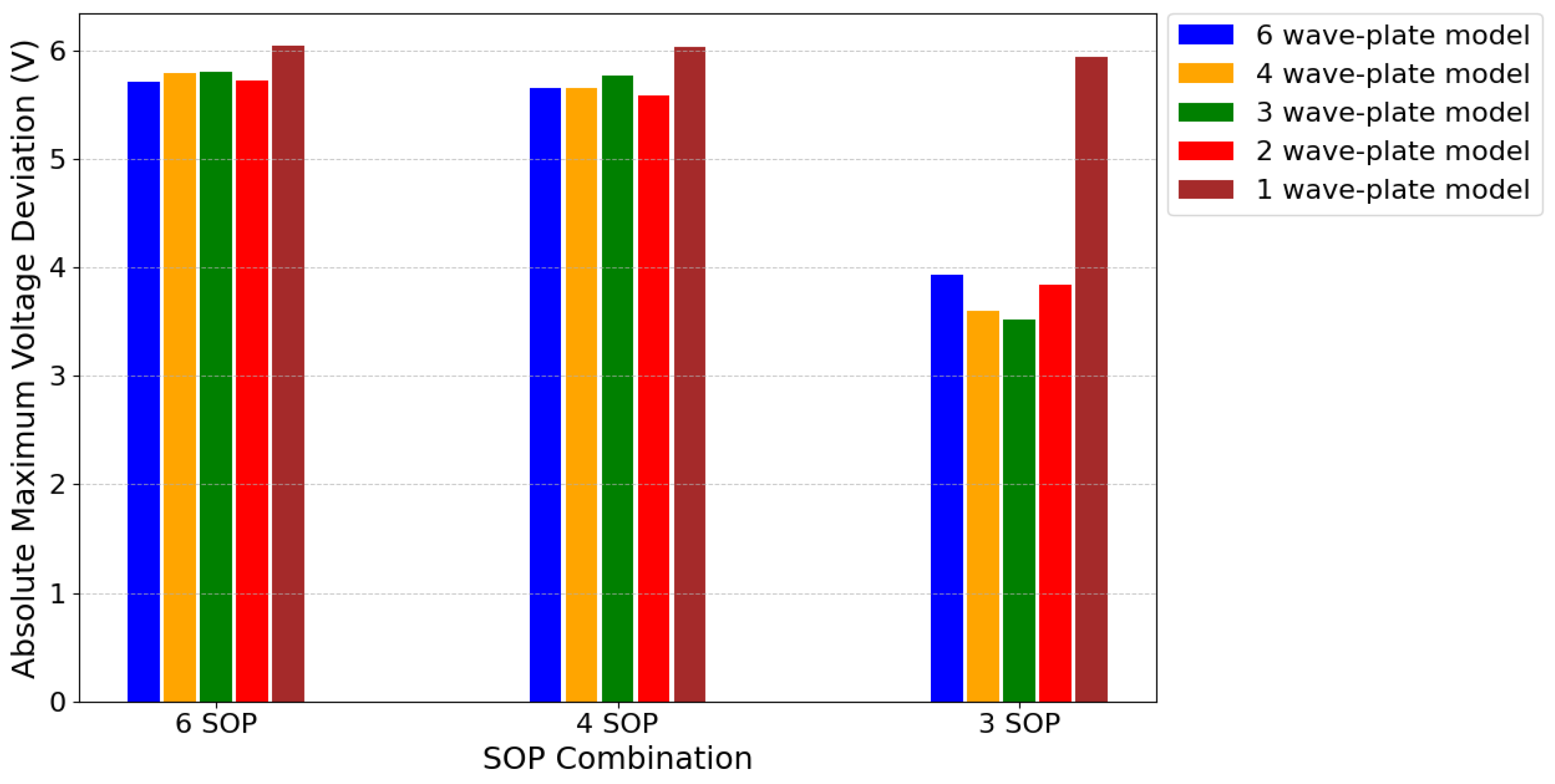
Based on these results, designing a driver capable of reaching all three bases, utilizing all available wave-plates, and accommodating the worst-case input polarization would require a voltage range of approximately V. The results in Figure 6 were obtained without splitting wave-plates, which means that when using all six wave-plates of a six-wave-plate model, all 12 independent variables are considered during the optimization process. The number of variables can be reduced using the method described in Section 3.3.
In Figure 7, we present the voltage maximum voltage deviations obtained for four, three, two, and one wave-plate simplified models, while keeping the proportions , , and , , and (HD) remains as the starting polarization state. We observe that reducing the number of independent variables does not significantly impact our optimization results, provided the model includes at least two wave-plates (four variables), as the changes remain within an acceptable margin of error for the algorithm. The results of a one wave-plate simplification are also a good starting point to obtain the overall expected requirements for both six and four SOP combinations.

Figure 7.
Absolute maximum voltage deviation as a function of the number of SOPs, using simplified models with one to four wave-plates, derived from a six-wave-plate EPC model.
Using this knowledge, we can also generate a graph such as Figure 6 after calculating the and values for a simplified model, such as for one wave-plate. The values and remain fixed for each individual wave-plate regardless of the number of wave-plates used in the six-wave-plate EPC model.
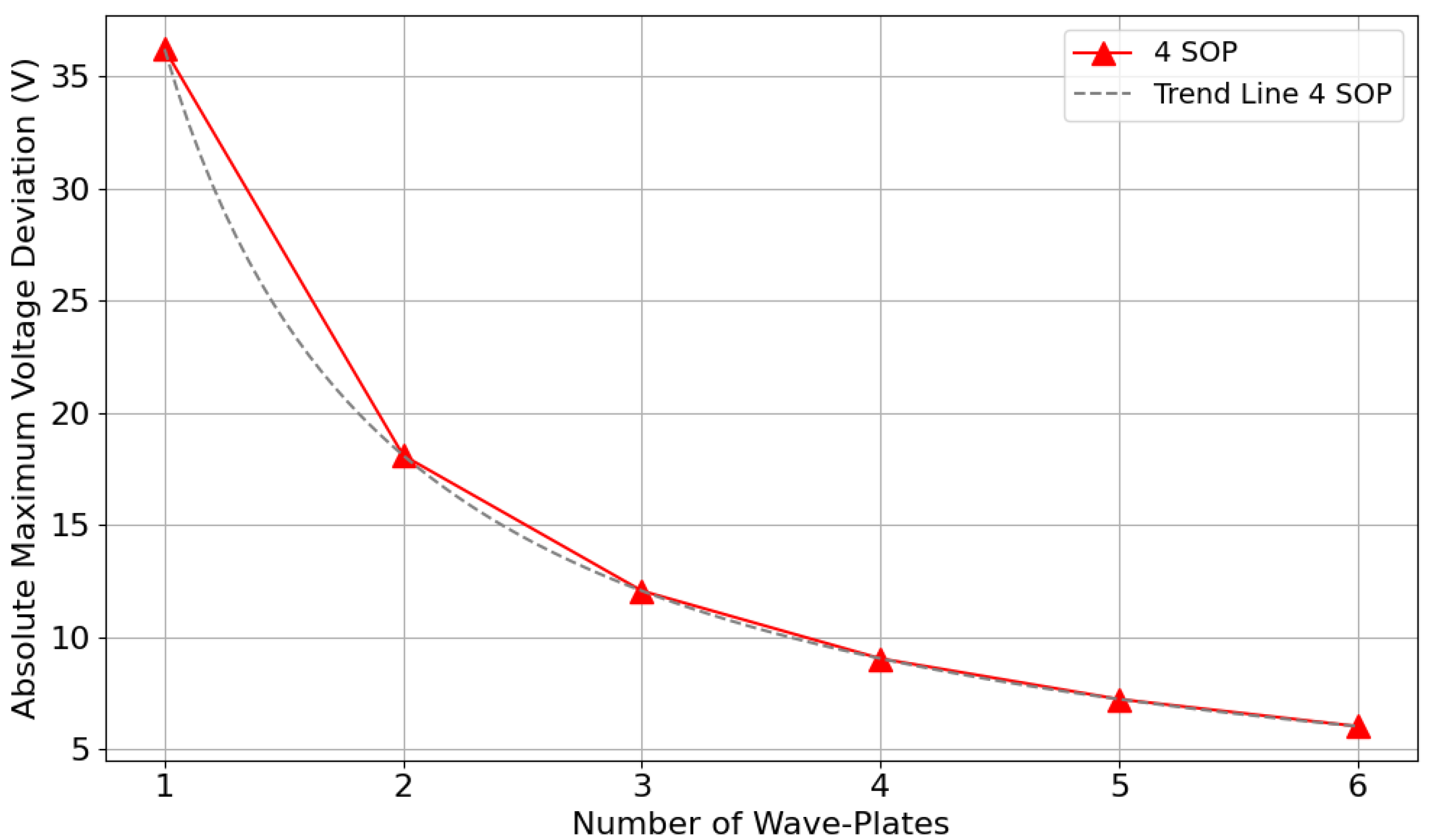
Figure 8 shows the results of wave-plate splitting, through the use of a one wave-plate simplified model, according to the number of wave-plates used from the six available. The associated trend line follows the equation , since we evenly divided over the respective number of wave-plates used. The multiplication factor corresponds to the maximum deviation observed when using only one wave-plate in the six-wave-plate model. The trend also closely resembles the one presented in Figure 6, for four SOP. This same logic can be applied to a two-wave-plate simplification, where only the values for two, four, and six wave-plates would be included, as they are multiples of two. The two-wave-plate simplification would also provide more meaningful insights into the requirements for an implementation using only three SOPs.

Figure 8.
Absolute maximum voltage deviation from bias as a function of the number of wave-plates for a four SOP combination (two bases), obtained by splitting a simplified one-wave-plate model over a six-wave-plate EPC, where unused wave-plates are set to their associated values.
4.2. Optimization Surrounding Zero Volts
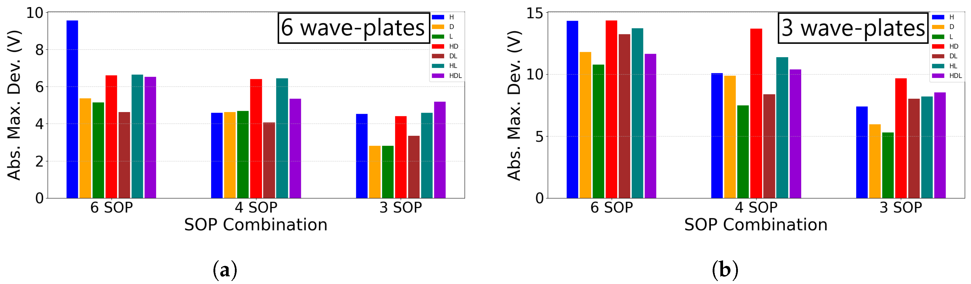
The optimization around zero volts, or ground, stems from an implementation expectation, as we consider this to be the midpoint of the electronic driver. Consequently, the results in this section depend on the bias voltages , specifically and in our case. Another assumption in this section is that any unused wave-plate in our six-wave-plate model is either left unconnected or connected to ground. Consequently, all unused wave-plates are characterized by and , as determined by our specific calibration parameters. The input polarization dependence results, shown in Figure 9 for three and six wave-plates, reveal that the relative magnitudes of each input SOP are not preserved across different wave-plate configurations. This trend remains consistent for other wave-plate combinations and can be attributed to additional polarization modulation introduced by unused wave-plates, which effectively alter the input SOP. Such alterations are absent if the unused wave-plates exhibit zero birefringence when not in use, as assumed in the previous section.

Figure 9.
Absolute maximum voltage deviation from zero, in relation to the input SOP and number of SOPs, using (a) six wave-plates of the six-wave-plate model and (b) three wave-plates of the six wave-plate model.
Nevertheless, we consider the SOP (HD) as a starting point once again, as, while it is not the worst-case scenario for six wave-plates, it is one of the worst input SOPs overall among the wave-plate configurations we tested.
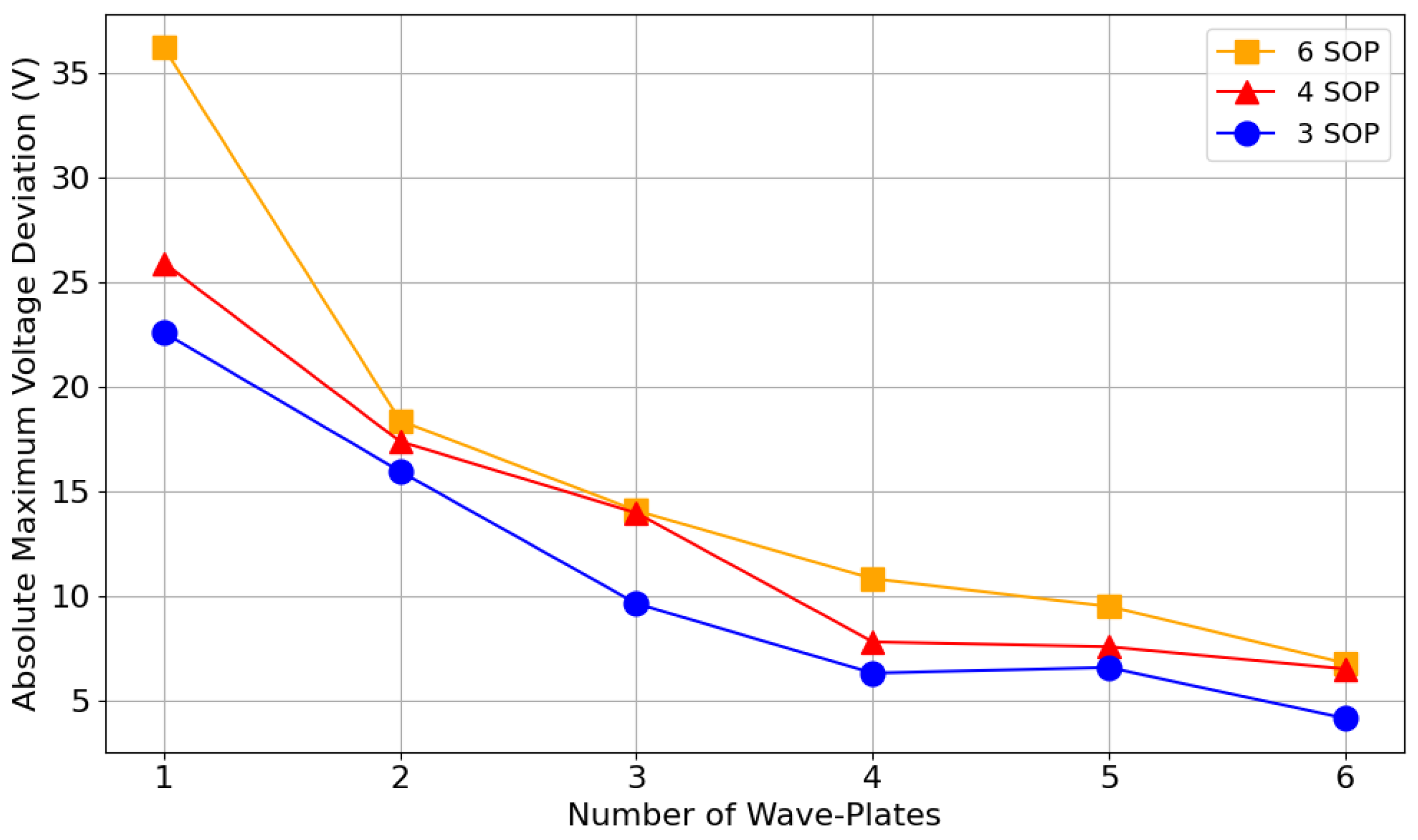
Figure 10 represents the absolute maximum voltage deviation from zero as a function of the number of wave-plates for different SOP combinations. It follows a trend resembling a negative power-law equation, similar to Figure 6, although less distinct. This weaker correlation between the number of wave-plates and voltage deviation aligns with the observations in Figure 9. As a result, Figure 10 shows that the voltage range for four wave-plates is comparable to that of five wave-plates, despite using fewer wave-plates, since the effective input SOP is more favorable. Based on these results, designing a driver capable of reaching all three bases while utilizing all wave-plates would require approximately . However, this does not represent the worst-case scenario for six wave-plates in particular, as shown in Figure 9a, where is needed to achieve all six SOPs when the input SOP is (H) rather than (HD). The same simplified model logic presented in Section 3.3 could also be applied here, with the caveat that the effects of the additional unused wave-plates must be taken into account and in the same order.

Figure 10.
Absolute maximum voltage deviation from zero, as a function of the number of wave-plates for different SOP combinations (three, four, and six SOPs), using a six-wave-plate EPC model, where unused wave-plates are connected to zero volts.
4.3. Voltage Swings
The limiting factor for the transition speeds between SOPs, besides electrical equipment limitations such as the slew rate, is the maximum voltage interval required to transition between two SOPs. This optimization is performed after obtaining results from either of the previous sections. We begin by using the values from the previous optimization procedure, whether surrounding the bias voltage points or zero, and identify the basis that requires the lowest voltage swing between its SOPs. Subsequently, we utilize a simplified variable model, such as with two or three wave-plates, to minimize the distance between the SOPs that compose the previously identified basis. After optimizing the voltage swing for the first basis, the average voltage values of the first basis are used as a reference, using (7) to optimize the second. For the third basis, the average voltage values of the two previously calculated bases are used as the reference.
The previous optimization procedure, whether surrounding the bias voltage points or zero, significantly impacts the achievable voltage swings. For instance, using all wave-plates in the six-wave-plate model and with an input SOP of (HLD), we calculate the transitions between the SOPs composing each basis (e.g., for the linear basis) within of the bias points, which result in transitions around . Achieving similar results surrounding zero would require expanding the driver range to . Interestingly, represents a relevant break point, because the values, which are close to , combined with the previous range, from the bias optimization, sum to the new limiting range of . This implies that the algorithm requires values closer to the bias, lower , to achieve comparable results. If the range is limited to surrounding zero, the transitions between SOPs within each basis increase to approximately 6 to .
In Figure 11, we provide a more in-depth analysis of the expected maximum voltage swings across multiple SOP combinations, surrounding bias, while considering all possible SOP transitions, and with the input SOP set to (HD). The smaller the absolute maximum voltage swing, the faster modulation can occur, thereby improving system efficiency. When utilizing all wave-plates in a six-wave-plate EPC model, it is expected that, among all six SOP transitions, the maximum voltage interval is approximately . This result falls within the range surrounding the bias points, presented in Section 4.1 The wave-plate splitting technique described in Section 3 was applied in Figure 11. Specifically, the results for four wave-plates were obtained by splitting a two-wave-plate simplified model, and the results for six wave-plates were obtained by splitting a three-wave-plate simplified model. Utilizing simplified models during this optimization proves even more advantageous than in the voltage range optimization, as each SOP jump might be optimized again following an update to the reference points in (7).
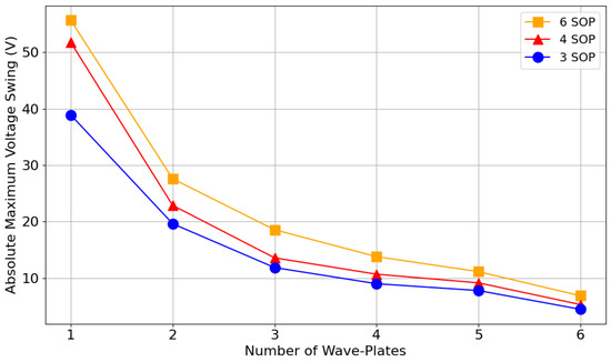
Figure 11.
Absolute maximum voltage swing between SOPs as a function of the number of wave-plates for different SOP combinations (three, four, and six SOPs), using a six-wave-plate EPC model, where unused wave-plates are set to their associated values.
5. Discussion and Conclusions
The results presented in this work are based on simulations and focus specifically on optimizing the generation of three SOP bases. The two optimization approaches analyzed, surrounding bias or zero volts, each have their own trade-offs. The bias-centered approach reduces the required modulation voltage but requires the driver to operate around offset voltages, which may be impractical in some hardware configurations. In contrast, the zero-centered approach ensures that unused wave-plates remain at zero voltage but introduces unwanted modulation effects, dependent on the number of wave-plates used. A potential solution for this issue involves performing a calibration step to identify the exact zero- birefringence points of the unused wave-plates.
The input SOP plays a crucial role in determining the overall voltage range required for modulation. In this work, we assumed a worst-case scenario for the input SOP; however, better-aligned starting points can reduce the required voltage range by up to 60%, depending on the SOP combination. The values of and , which are part of the physical characteristics and calibration parameters of the device, affect the sinusoidal behavior of and , shifting the values that correspond to the peaks of or , and therefore influencing the preferable combination for a given pair. Our findings indicate that reducing the number of independent wave-plates to two (four variables) achieves performance comparable to models with higher independent wave-plate counts, providing sufficient flexibility to optimize transitions while maintaining a balanced voltage range. While specific input SOPs and wave-plate count combinations may offer advantages for certain transitions, their impact diminishes when a complete SOP basis is required. Accordingly, we implemented a dedicated optimization framework to minimize the absolute voltage range, for each of the three SOP bases. Using this framework, we determined that achieving all six SOPs requires a voltage range of when centering operations around bias voltage points and when centering around zero volts. Additionally, the maximum voltage swing between SOPs was evaluated, yielding a value of . These results confirm that a minimal set of control parameters can still deliver efficient system performance.
While the optimization framework provides an efficient way to determine the best voltage settings, it does not incorporate an active polarization drift compensation mechanism. This means that external polarization fluctuations, such as those caused by fiber birefringence changes over time, are not corrected within this optimization framework. In long-distance optical fiber channels, these dynamic variations could impact system stability on the receiver side, requiring additional real-time compensation methods. Separately, long-term environmental fluctuations, including temperature variations, mechanical strain, and electrical noise can cause voltage drift in -based modulators [31], necessitating periodic recalibration. In practical applications, this issue must be addressed through active feedback control to maintain stable performance.
The results presented here have significant implications for the development of QKD systems, enabling faster modulation speeds, reduced hardware complexity, and enhanced system efficiency. The proposed framework can be adapted to various EPC models, making it a versatile tool for advancing polarization-based QKD protocols. These findings will contribute to the widespread adoption of efficient polarization control in polarization-based QKD subsystems. Future research will focus on implementing the optimization algorithm in a real-time polarization feedback loop and assessing its performance in practical QKD systems.
Author Contributions
Conceptualization, H.F.C. and N.J.M.; Methodology, H.F.C. and N.J.M.; Software, H.F.C.; Formal analysis, H.F.C.; Investigation, H.F.C.; Data curation, H.F.C.; Writing—original draft, H.F.C.; Writing—review and editing, A.N.P. and N.J.M.; Visualization, H.F.C.; Supervision, A.N.P. and N.J.M.; Project administration, A.N.P. and N.J.M.; Funding acquisition, A.N.P. and N.J.M. All authors have read and agreed to the published version of the manuscript.
Funding
This research was funded by FCT under projects QuantERA/0001/2021 and Ph.D. Grant 2023.01100.BD. Additionally, it received support from the EU QuantERA program (GA 101017733) and the EU DIGITAL-2021-QCI-01 Programme, thought the project PTQCI (GA 101091730).
Institutional Review Board Statement
Not applicable.
Informed Consent Statement
Not applicable.
Data Availability Statement
Data underlying the results presented in this paper are not publicly available but may be obtained from the authors upon reasonable request.
Conflicts of Interest
The authors declare no conflict of interest.
References
- Boudot, F.; Gaudry, P.; Guillevic, A.; Heninger, N.; Thomé, E.; Zimmermann, P. The State of the Art in Integer Factoring and Breaking Public-Key Cryptography. IEEE Secur. Priv. 2022, 20, 80–86. [Google Scholar] [CrossRef]
- Wei, S.H.; Jing, B.; Zhang, X.Y.; Liao, J.Y.; Yuan, C.Z.; Fan, B.Y.; Lyu, C.; Zhou, D.L.; Wang, Y.; Deng, G.W.; et al. Towards real-world quantum networks: A review. Laser Photon. Rev. 2022, 16, 2100219. [Google Scholar] [CrossRef]
- Muga, N.; Ramos, M.; Mantey, S.; Silva, N.; Pinto, A. FPGA-assisted state-of-polarization generation for polarization-encoded optical communications. IET Optoelectron. 2020, 14, 350–355. [Google Scholar] [CrossRef]
- Liao, S.K.; Cai, W.Q.; Liu, W.Y.; Zhang, L.; Li, Y.; Ren, J.G.; Yin, J.G.; Shen, Q.; Cao, Y.; Li, Z.P.; et al. Satellite-to-ground quantum key distribution. Nature 2017, 549, 43–47. [Google Scholar] [CrossRef] [PubMed]
- Liao, S.K.; Yong, H.L.; Liu, C.; Shentu, G.L.; Li, D.D.; Lin, J.; Dai, H.; Zhao, S.Q.; Li, B.; Guan, J.Y.; et al. Long-distance free-space quantum key distribution in daylight towards inter-satellite communication. Nat. Photonics 2017, 11, 509–513. [Google Scholar] [CrossRef]
- Agnesi, C.; Avesani, M.; Calderaro, L.; Stanco, A.; Foletto, G.; Zahidy, M.; Scriminich, A.; Vedovato, F.; Vallone, G.; Villoresi, P. Simple quantum key distribution with qubit-based synchronization and a self-compensating polarization encoder. Optica 2020, 7, 284–290. [Google Scholar] [CrossRef]
- Mantey, S.; Silva, N.; Pinto, A.; Muga, N. Design and implementation of a polarization-encoding system for quantum key distribution. J. Opt. 2024, 26, 075704. [Google Scholar] [CrossRef]
- Williams, J.; Suchara, M.; Zhong, T.; Qiao, H.; Kettimuthu, R.; Fukumori, R. Implementation of quantum key distribution and quantum clock synchronization via time bin encoding. Proc. SPIE 2021, 11699, 16–25. [Google Scholar]
- Boaron, A.; Korzh, B.; Houlmann, R.; Boso, G.; Rusca, D.; Gray, S.; Li, M.J.; Nolan, D.; Martin, A.; Zbinden, H. Simple 2.5 GHz time-bin quantum key distribution. Appl. Phys. Lett. 2018, 112, 171108. [Google Scholar] [CrossRef]
- Liang, W.Y.; Wang, S.; Li, H.W.; Yin, Z.Q.; Chen, W.; Yao, Y.; Huang, J.Z.; Guo, G.C.; Han, Z.F. Proof-of-principle experiment of reference-frame-independent quantum key distribution with phase coding. Sci. Rep. 2014, 4, 1–6. [Google Scholar] [CrossRef]
- Bennett, C.H.; Brassard, G. Quantum Cryptography: Public Key Distribution and Coin Tossing. In Proceedings of the IEEE International Conference on Computers, Systems and Signal Processing, Bangalore, India, 10–12 December 1984; pp. 175–179. [Google Scholar]
- Yan, Z.; Meyer-Scott, E.; Bourgoin, J.P.; Higgins, B.L.; Gigov, N.; MacDonald, A.; Hübel, H.; Jennewein, T. Novel High-Speed Polarization Source for Decoy-State BB84 Quantum Key Distribution Over Free Space and Satellite Links. J. Light. Technol. 2013, 31, 1399–1408. [Google Scholar] [CrossRef]
- Liu, X.; Liao, C.; Tang, Z.; Wang, J.; Wei, Z.; Liu, S. Polarization coding and decoding by phase modulation in polarizing sagnac interferometers. Proc. SPIE 2007, 6827, 68270I. [Google Scholar]
- Duplinskiy, A.; Ustimchik, V.; Kanapin, A.; Kurochkin, V.; Kurochkin, Y. Low loss QKD optical scheme for fast polarization encoding. Opt. Express 2017, 25, 28886. [Google Scholar] [CrossRef]
- Wang, J.; Qin, X.; Jiang, Y.; Wang, X.; Chen, L.; Zhao, F.; Wei, Z.; Zhang, Z. Experimental demonstration of polarization encoding quantum key distribution system based on intrinsically stable polarization-modulated units. Opt. Express 2016, 24, 8302–8309. [Google Scholar] [CrossRef] [PubMed]
- Comandar, L.C.; Fröhlich, B.; Lucamarini, M.; Patel, K.A.; Sharpe, A.W.; Dynes, J.F.; Yuan, Z.L.; Penty, R.V.; Shields, A.J. Room temperature single-photon detectors for high bit rate quantum key distribution. Appl. Phys. Lett. 2014, 104, 021101. [Google Scholar] [CrossRef]
- Chen, S.; You, L.; Zhang, W.; Yang, X.; Li, H.; Zhang, L.; Wang, Z.; Xie, X. Dark counts of superconducting nanowire single-photon detector under illumination. Opt. Express 2015, 23, 10786–10793. [Google Scholar] [CrossRef] [PubMed]
- Xiao-Bao, L.; Chang-Jun, L.; Zhi-Lie, T.; Jin-Dong, W.; Song-Hao, L. Quantum Key Distribution System with Six Polarization States Encoded by Phase Modulation. Chin. Phys. Lett. 2008, 25, 3856. [Google Scholar] [CrossRef]
- Xi, L.; Zhang, X.; Tian, F.; Tang, X.; Weng, X.; Zhang, G.; Li, X.; Xiong, Q. Optimizing the operation of LiNbO3-based multistage polarization controllers through an adaptive algorithm. IEEE Photonics J. 2010, 2, 195–202. [Google Scholar]
- Shan, L.; Lu, Q.; Sun, P.; Zhang, X.; Xi, L.; Xiao, X. Calibration of LiNbO3- based polarization controller with simplified principle and RMSProp algorithm. In Proceedings of the 2023 Asia Communications and Photonics Conference/2023 Photonics and Optoelectronics Meetings (ACP/POEM), Wuhan, China, 4–7 November 2023; pp. 1–3. [Google Scholar]
- Garcia, J.D.; Amaral, G.C. An optimal polarization tracking algorithm for Lithium-Niobate-based polarization controllers. In Proceedings of the 2016 IEEE Sensor Array and Multichannel Signal Processing Workshop (SAM), Rio de Janeiro, Brazil, 10–13 July 2016. [Google Scholar]
- Hou, Q.; Yuan, X.; Zhang, Y.; Zhang, J. Endless polarization stabilization control for optical communication systems. Chin. Opt. Lett. 2014, 12, 110603. [Google Scholar]
- Xavier, G.B.; Walenta, N.; Vilela de Faria, G.; Temporão, G.P.; Gisin, N.; Zbinden, H.; von der Weid, J.P. Experimental polarization encoded quantum key distribution over optical fibres with real-time continuous birefringence compensation. N. J. Phys. 2009, 11, 045015. [Google Scholar] [CrossRef]
- Costa, H.; Muga, N.J.; Silva, N.A.; Pinto, A.N. Advanced Algorithms for Optimization of QKD Encoding Subsystems. In Proceedings of the International Conference on Applications of Optics and Photonics—AOP2014, Aveiro, Portugal, 16–19 July 2024. [Google Scholar]
- Gunantara, N. A review of multi-objective optimization: Methods and its applications. Cogent Eng. 2018, 5, 1502242. [Google Scholar] [CrossRef]
- Deb, K.; Pratap, A.; Agarwal, S.; Meyarivan, T. A fast and elitist multiobjective genetic algorithm: NSGA-II. IEEE Trans. Evol. Comput. 2002, 6, 182–197. [Google Scholar] [CrossRef]
- van Haasteren, A.; van der Tol, J.; van Deventer, M.; Frankena, H. Modeling and characterization of an electrooptic polarization controller on LiNbO3. J. Light. Technol. 1993, 11, 1151–1157. [Google Scholar] [CrossRef]
- EOSPACE. Polarization Controller Calibration Data; User’s Manual; EOSPACE: Redmond, WA, USA, 2014. [Google Scholar]
- Goldstein, D.H. Polarized Light, 3rd ed.; CRC Press: Boca Raton, FL, USA, 2011. [Google Scholar]
- Blank, J.; Deb, K. pymoo: Multi-Objective Optimization in Python. IEEE Access 2020, 8, 89497–89509. [Google Scholar] [CrossRef]
- Salvestrini, J.P.; Guilbert, L.; Fontana, M.; Abarkan, M.; Gille, S. Analysis and Control of the DC Drift in LiNbO3-Based Mach–Zehnder Modulators. J. Light. Technol. 2011, 29, 1522–1534. [Google Scholar] [CrossRef]
Disclaimer/Publisher’s Note: The statements, opinions and data contained in all publications are solely those of the individual author(s) and contributor(s) and not of MDPI and/or the editor(s). MDPI and/or the editor(s) disclaim responsibility for any injury to people or property resulting from any ideas, methods, instructions or products referred to in the content. |
© 2025 by the authors. Licensee MDPI, Basel, Switzerland. This article is an open access article distributed under the terms and conditions of the Creative Commons Attribution (CC BY) license (https://creativecommons.org/licenses/by/4.0/).