Article

Quantum-Well-Embedded InGaN Quantum Dot Vertical-Cavity Surface-Emitting Laser and Its Photoelectric Performance

1
Key Laboratory of Interface Science and Engineering in Advanced Materials of Ministry of Education, Taiyuan University of Technology, Taiyuan 030024, China
2
Shanxi-Zheda Institute of Advanced Materials and Chemical Engineering, Taiyuan 030024, China
3
Xi’an Key Laboratory of Compound Semiconductor Materials and Devices, School of Physics & Information Science, Shaanxi University of Science and Technology, Xi’an 710021, China
*
Author to whom correspondence should be addressed.
Photonics 2025, 12(3), 276; https://doi.org/10.3390/photonics12030276
Submission received: 10 February 2025 / Revised: 6 March 2025 / Accepted: 7 March 2025 / Published: 17 March 2025
(This article belongs to the Section Lasers, Light Sources and Sensors)

Abstract

:
An electrically injected vertical-cavity surface-emitting laser (VCSEL) with quantum-well-embedded InGaN quantum dots (QDs) as the active region was designed. The InGaN QD size and cavity length were optimized using PICS3D simulation software to achieve a high-performance InGaN QD-embedded VCSEL. A comparative analysis between the InGaN QD VCSEL and the traditional InGaN quantum well VCSEL was conducted, and the results demonstrated that the InGaN QD VCSEL achieved higher stimulated recombination radiation and internal quantum efficiency. The threshold current was reduced to 4 mA, corresponding to a threshold current density of 5.1 kA/cm², and the output power reached 4.4 mW at an injection current of 20 mA. A stable single-longitudinal-mode output was also achieved with an output wavelength of 436 nm. The proposed novel quantum-well-embedded QD active-region VCSEL was validated through theoretical simulations, confirming its feasibility. This study provides theoretical guidance and key epitaxial structural parameters for preparing high-performance VCSEL epitaxial materials.

1. Introduction

The GaN-based vertical-cavity surface emitting laser (VCSEL), as a new type of semiconductor laser associated with low power consumption, a low threshold current, inherent single-longitudinal-mode operation, and a circular beam shape, is easy to fiber-couple and integrate into two-dimensional arrays, as well as having many other unique advantages [1]. The development of the GaN-based blue-green VCSEL differs from that of GaAs [2] and InP material systems, being relatively slow [3,4].
Many challenges limit VCSEL devices’ performance, such as the fact that the GaN-based VCSEL usually adopts InGaN quantum wells as the active region. This is attributed to the fact that the crystal structures of GaN and InGaN, when grown on a sapphire substrate in the [0001] direction of the wurtzite structure, exhibit spontaneous polarization effects in the wurtzite nitride semiconductor [5]. In addition to the spontaneous polarization effect [6], GaN and InGaN heterojunction structures also have piezoelectric polarization effects, and both jointly influence the development of the GaN-based VCSEL. Significant progress has been made in InGaN quantum wells in recent years due to their ability to capture electrons and holes in the active region effectively. However, studies have found that InGaN quantum wells have high radiative recombination, which is attributed to the strong quantum-confined Stark effect caused by the material [7], and the effective mass of the hole in the InGaN material is much larger than that of the electron; the large effective mass of carriers in the GaN-based material system results in a high transparent carrier concentration [8]. GaN-based quantum wells in the growth process [9], owing to significant lattice mismatches, will produce many defects. With the continuous development and progress made in epitaxial growth technology, QD materials are increasingly being inserted into active regions. Studies have found that introducing QDs can improve quantum efficiency, even in the presence of many defects in materials [10]. Numerous experiments have shown that InGaN phase separation can form In-rich clusters in quantum wells [11]; these small clusters can be regarded as InGaN QDs, which can effectively suppress the influence of defects and improve the luminescence efficiency. During the growth of QDs in the Stranski–Krastanow growth mode, the strain present in the film is the driving force for the formation of QDs [12]. The growth of QDs is accompanied by strain relaxation [13]. The piezoelectric polarization field in QDs and the quantum-confined Stark effect are almost eliminated [14]. QDs are zero-dimensional materials in which electrons and holes are well confined in a small space, resulting in a δ-function-like state density [15], which is important for realizing low threshold current densities. Meanwhile, the strong localization effect of QDs [16] can effectively prevent carriers from being trapped by nonradiative recombination centers and improve the light excitation efficiency in the active region [17]. Therefore, InGaN QDs have become another research hotspot.
In order to improve the photoelectric performance of GaN-based devices, InGaN QDs, used as the active region of new-generation photoelectric devices, have seen rapid development. L. Ji et al. prepared InGaN/GaN multi-QD blue LEDs using metal–organic chemical vapor deposition with a voltage of 3.1 V, which is lower than that of traditional quantum well LEDs with a forward voltage of 3.5 V [18]. M. Zhang et al. prepared a 524 nm laser diode with an InGaN self-assembled QD active region using metal–organic chemical vapor deposition and successfully achieved excitation under electrical injection with a threshold current density of 1.2 kA/cm2, and the output power was 1.7 mW at a current density of 3 kA/cm2 [19]. G. Weng et al. utilized InGaN QDs instead of quantum wells as the active region to obtain room-temperature continuous excitation at a yellow-green wavelength of 560.4 nm for the first time for the GaN-based VCSEL, obtaining a threshold current density of 0.78 kA/cm2 and a maximum output power of 5.9 μW [20]. Y. Mei et al. successfully achieved room-temperature multiple longitudinal mode emission in a GaN-based green VCSEL by changing the resonant cavity length using an all-dielectric film distributed Bragg reflector (DBR) [21]. The device was successfully obtained by changing the resonant cavity length. The wavelength ranges from 479.6 to 565.7 nm, filling the “green gap” of GaN-based light-emitting devices [22]. The threshold current density is as low as 0.66 kA/cm2, and the maximum output power is 4.8 μW. Meanwhile, the metal bonding process is utilized to improve the heat dissipation performance effectively. T. Yang et al. utilized InGaN QDs as the active region and achieved a stable excitation peak at 524.0 nm with improved thermal stability of the VCSEL [23]; the threshold current density of VCSEL emitted at 524.0 nm was 51.97 A/cm2 and the internal quantum efficiency (IQE) reached 69.94%. Based on the advantages of reducing the threshold current density and increasing the output power of InGaN QDs, the growth technology of InGaN QDs has been continuously improved in recent years, and a high-performance InGaN QD VCSEL has been prepared to reduce threshold current density. However, the output power is still low, and a single-longitudinal-mode output cannot be achieved at different current densities. Therefore, further studies on the internal carrier transport [24], the IQE, and its photoelectric properties in the InGaN QD active region are needed to obtain high-performance QD GaN-VCSEL [25].
The epitaxial structure, composition, and dimensions of the active region of the quantum-well-embedded QDs are optimized using PICS3D 2024 simulation software. The production of quantum-well-embedded QDs is carried out. The epitaxial structure of the optical resonant cavity is optimized. The resonance wavelength is adjusted, and the parameters of the optical resonance cavity are determined by simulation to achieve stable single-longitudinal-mode excitation at 436 nm. The GaN-VCSEL is designed with a SiO2 burial structure. The energy band, photoelectric performance output characteristics, and optical modes of the QD-VCSEL and traditional GaN-VCSEL are comparatively analyzed.
In this study, we address the limitations of conventional InGaN quantum well VCSELs by proposing a quantum-well-embedded QD active region design. The following sections elaborate on the device design, simulation methodologies, and performance evaluation. Section 2 outlines the structural optimization of the VCSEL, including epitaxial parameters and cavity configuration. Section 3 employs PICS3D simulations to analyze energy band, recombination mechanisms, and transverse optical modes, validating the enhanced photoelectric characteristics. Section 4 concludes with key advancements in threshold current reduction, output power improvement, and stable single-longitudinal-mode operation, providing critical insights for future high-performance GaN-VCSEL development.

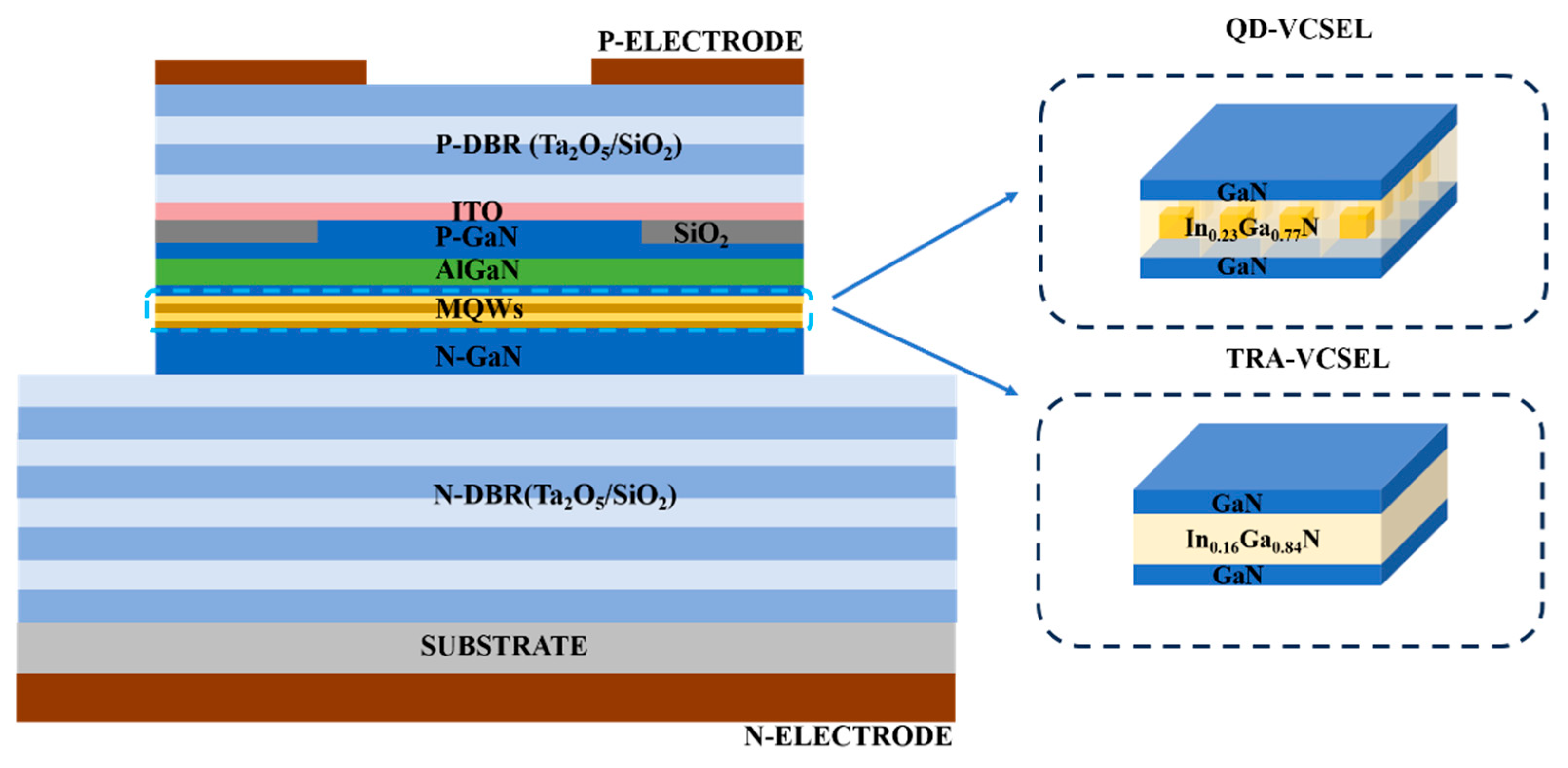
2. VCSEL Device Design

A VCSEL with quantum-well-embedded InGaN QD structures was designed in this work, as shown in Figure 1. The VCSEL mainly consists of N-type Ta2O5/SiO2 DBR, an active region of multiple quantum wells (MQWs), and P-type Ta2O5/SiO2 DBR. The active region of a traditional VCSEL consists of a 6 nm thick GaN barrier layer and a 2.5 nm thick In0.16Ga0.84N well layer, and the thin MQWs are used because they can have a strong coupling effect with the optical field and thus obtain a better optical confinement factor. The designed quantum-well-embedded QD structure consists of a 6 nm thick GaN base layer wrapper, a 0.75 nm thick In0.16Ga0.84N-well layer wrapper, and a 1 nm thick In0.23Ga0.77N QD structure, and the right-hand figure shows the structure of two single-layer quantum wells. The VCSEL is composed of alternately dual dielectric DBR materials Ta2O5/SiO2 [26], where P-DBR consists of 10 pairs and N-DBR consists of 12 pairs of double dielectric DBR materials. A 20 nm thick indium tin oxide (ITO) current spreading layer is employed, and a 10 nm thick SiO2 layer is used as the current confinement layer. The device has an optical emission aperture (current confinement aperture) with a diameter of 5 µm, and the cavity length of the VCSEL is 16 λ. The VCSEL with a QD-embedded structure was defined as QD-VCSEL, and the VCSEL with a traditional structure was defined as TRA-VCSEL. The detailed structural parameters are provided in Table 1 under optimal device performance conditions.
In order to investigate the electrical and optical characteristics of the high-performance QD GaN-VCSEL, the PICS3D simulation software was used. This software is based on three-dimensional finite element analysis with a 6×6 k·p model, which can calculate and solve the current continuity equations, drift–diffusion equations, and Schrödinger and Poisson’s equations of the VCSEL in the cylindrical coordinate system [27]. The transport model includes electrons and holes. The transport model includes electron and hole drift and diffusion, Fermi statistics, and Shockley–Read–Hall (SRH) recombination of spontaneous and defect-related carriers [28]. Because strain relaxation needs to be considered during epitaxial growth and affects the spontaneous and piezoelectric polarization of GaN-based material, it is necessary to set the polarization level to 40% [29]. Considering that other recombinations will occur at the defects, it is also necessary to set the Auger and SRH recombination coefficients in the material. Due to the existence of two heterojunctions (InGaN/InGaN and GaN/AlGaN), it is necessary to set the conduction band and valence band offset ratios for both interfaces [30]. To make the simulation results more realistic, the average optical background loss should be set to 1000 m−1, as shown in Table 2. When calculating the optical model, the effective refractive index model must be used [31]. To solve the longitudinal and transverse modes for calculating cylindrically symmetric VCSEL, the simulation model can be simplified into a two-bit axisymmetric structure to simplify the calculation process of the software.
Because of the small dimension of the InGaN QD, a separate modeling calculation is required for a separate QD structure, and the QD material must be defined as an embedded (or mildly active) material within the quantum well, acting as a wetting layer [32]. In the PICS 3D, we first model a single QD with an embedded quantum well structure in a subfile. Then, in the main file, we apply this model to specific quantum wells. The spacing between the QD is fixed at 10 nm. Considering the strong localization effect of QD materials and the fact that only QD materials can hinder the injection efficiency of charge carriers in quantum wells, we use thin GaN barrier layers and thin In0.16Ga0.84N barrier layers to increase the tunneling probability of charge carriers in each quantum well [33]. In order to obtain a low number of transparent carriers [34] and to mitigate the uneven distribution of carriers within the quantum wells, two pairs of quantum wells are employed as part of the active region. Additionally, to improve the utilization of carriers and reduce the quantum-confined Stark effect in this paper, the QD structure is modeled as a two-layer GaN barrier layer wrapped around an In0.16Ga0.84N quantum well acting as a wetting layer. In0.23Ga0.77N with a dimensional height degree of 1 nm is used in the QDs; the QD width set to 2 nm is more suitable for simulation calculations. In the simulation, we consider the QDs to be embedded within the quantum well. The size and distribution of these QDs are critical to the performance. However, in reality, the distribution and size of QDs can vary due to factors such as material composition and growth conditions. Inhomogeneous distribution of QD sizes is indeed a common characteristic of QDs grown in the Stranski–Krastanov mode, and this can affect the device’s performance. If the size distribution of the QDs is too broad, it can lead to inhomogeneous strain relaxation, which may reduce the overall carrier localization efficiency and internal quantum efficiency (IQE). The simulation assumes a relatively uniform size for simplicity. The growth method can be precisely controlled to regulate the distribution and size of the QDs in practice. The epitaxial wafer was grown on a c-plane (0001) sapphire substrate using an MOCVD system. The InGaN QD layers were grown as the active region via the Stranski–Krastanow growth mode. During the growth process, triethylgallium (TEGa) and trimethylindium (TMIn) were used as precursors for Ga and In sources, respectively. Ammonia (NH3) served as the nitrogen source, with hydrogen (H2) as the carrier gas for growing the GaN template and nitrogen (N2) for the QDs. The InGaN QDs were deposited at 670 °C with a molar gas phase ratio of TMIn/(TMIn + TEGa) of approximately 1:2, and the V/III ratio was set to 1.35 × 10⁴. After QD deposition, a two-step growth process was applied to grow the GaN cap layers. These controlled parameters allowed for the optimization of QD distribution and size, which are crucial for improving device performance. Detailed structural parameters of the quantum-well-embedded InGaN QD structure are shown in Table 3.

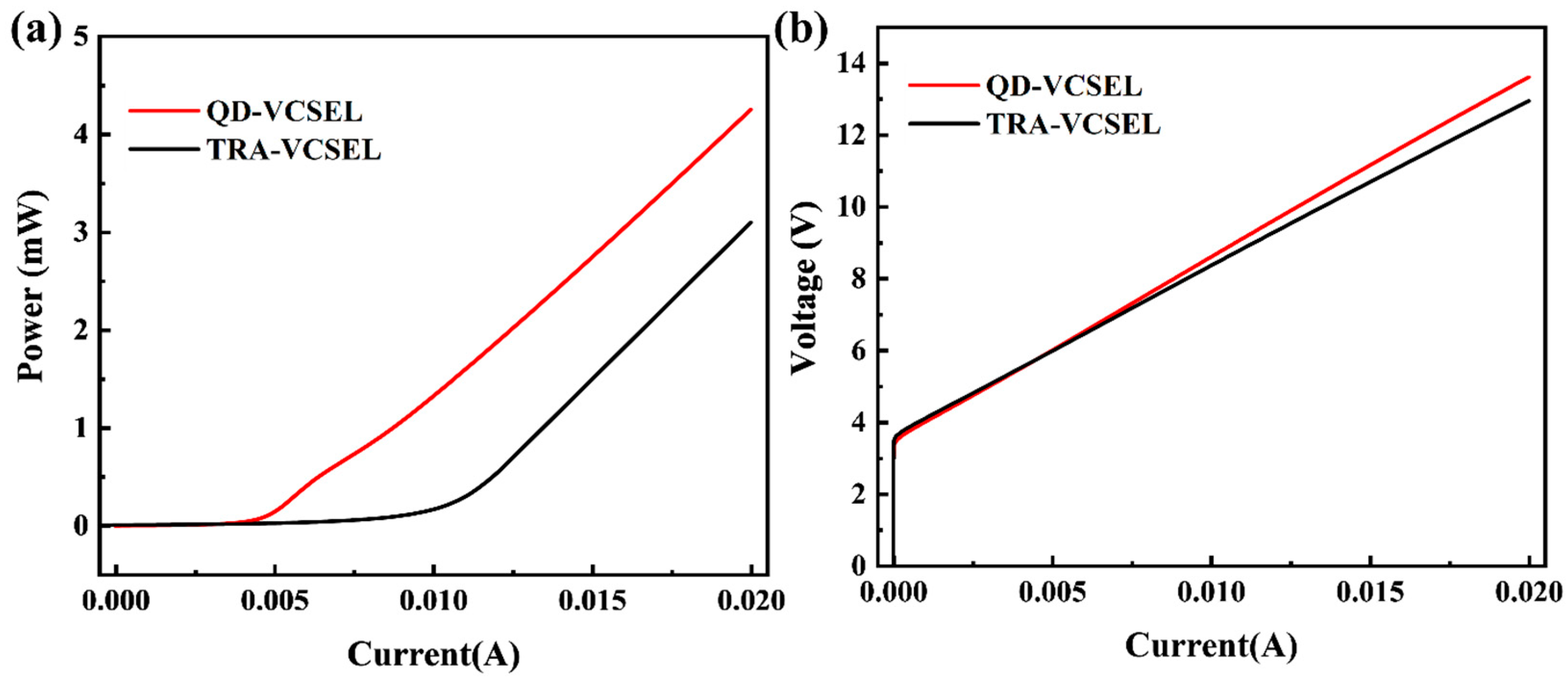
3. Simulation Results Analysis

The threshold current and operating voltage are the key parameters of the high-power GaN-based VCSEL, and Figure 2 shows the variations in the photoelectric characteristics of the QD-VCSEL and TRA-VCSEL with a 5 μm oxide aperture at 300 K with the injection current. As shown in Figure 2a, the threshold currents of the two VCSELs are 4 mA and 11 mA and the threshold current densities are 5.1 kA/cm2 and 14 kA/cm2, respectively, indicating that the threshold current decreases by 7 mA with the addition of the QD-embedded structure at an injection current of 20 mA, while the output power of the QD-VCSEL reaches 4.2 mW, which is higher than that of the TRA-VCSEL. With the addition of the QD-embedded structure, the output power increases by 26.1%. It is worth noting that there is no difference in voltage between them in terms of operating voltage; only the difference in the subsequent growth trend of QD-VCSEL is faster than that of TRA-VCSEL, which is attributed to the increase in the overall resistance owing to the QD layer and the wetting layer in the QD-VCSEL. The P-I and V-I plots illustrate that the performance of the QD-VCSEL is significantly improved, mainly due to the QD-embedded structure, which reduces the quantum-confined Stark effect and increases quantum efficiency.

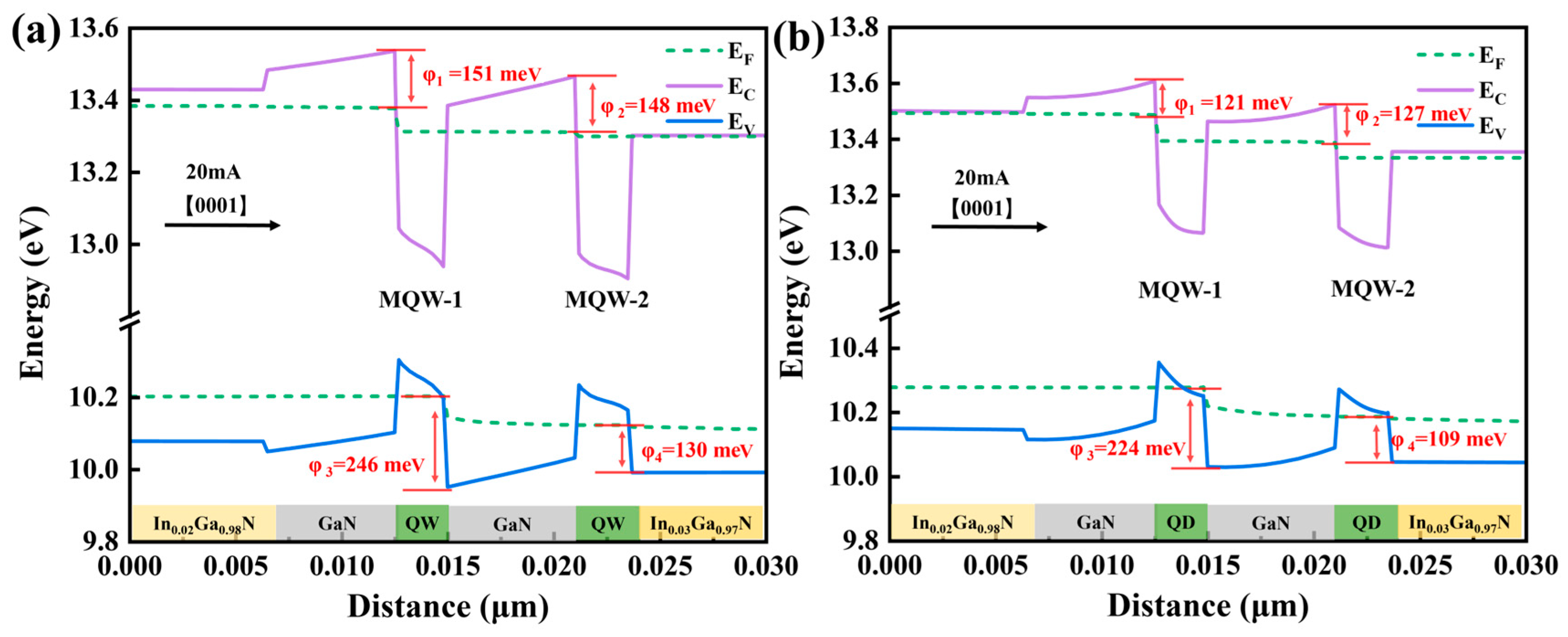
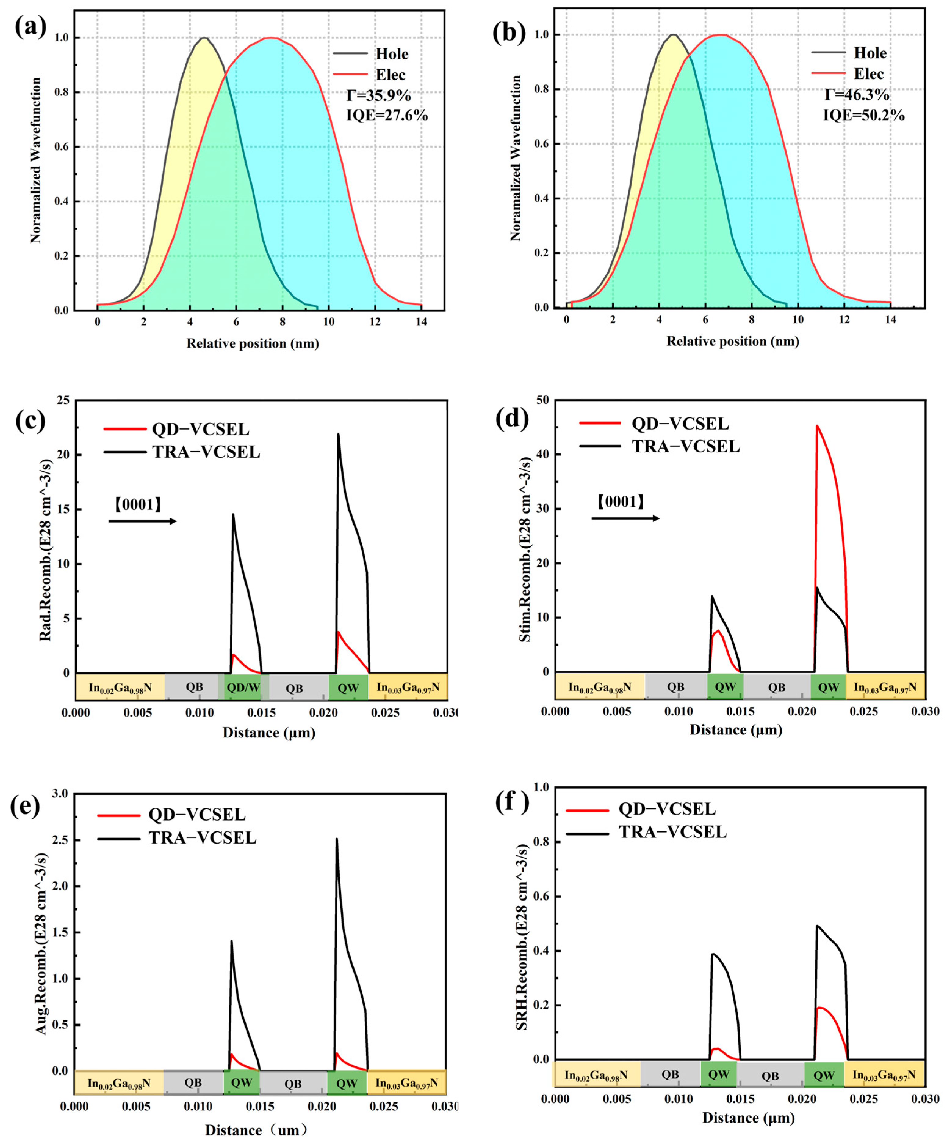
3.1. Energy Band Diagram of the Active Region

The QD-embedded structure has the most significant influence on the energy band, and the changes in the energy band are the most important cause of performance changes. By analyzing the energy band in the active region, it can be found that the height of the barrier affects the injection efficiency of the QD-VCSEL. Figure 3a,b show the energy bands of the TRA-VCSEL and QD-VCSEL in the [0001] direction at an injection current of 20 mA. The quantum well near the N-side is defined as MQW-1. The quantum well near the P-side is defined as MQW-2. The electron injection barrier φ1 is 151 meV for MQW-1 of the TRA-VCSEL, as shown in Figure 3a, while the electron injection barrier φ2 is 148 meV for MQW-2; the hole injection barrier φ3 is 246 meV for MQW-1, and that of MQW-2 is 130 meV. It can be seen that the electron injection barriers of the two quantum wells are similar. However, the difference in hole injection barriers is 116 meV, which indicates that holes are more readily injected into MQW-2 to undergo radiative recombination. The holes in MQW-1 will escape more readily into MQW-2. Figure 3b shows that the electron injection barrier φ1 of MQW-1 of the QD-VCSEL is 121 meV, the electron injection barrier φ2 of the second quantum well is 127 meV, the hole injection barrier φ3 of MQW-1 is 224 meV, and the hole injection barrier φ4 of MQW-2 is 109 meV. A comparison of the injection potential barriers shows that the QD-VCSEL has lower barrier heights than the TRA-VCSEL in terms of electron and hole injection barriers. The barrier height of the QD-VCSEL is lower than that of the TRA-VCSEL, which indicates that both electrons and holes are more easily injected into the quantum well, which is mainly caused by the introduction of the embedded QDs eliminating the piezoelectric polarization in the MQW. Thus, the introduction of QDs effectively reduces the barrier height and improves the carrier injection efficiency.
The disparity in energy band structures is primarily attributed not only to variations in potential barrier height but also to the quantum-confined Stark effect induced by the elevated indium composition. This effect causes the tilt of the energy band, and the piezoelectric polarization electric field of the QD in the active region is smaller than that of quantum wells. QDs are zero-dimensional materials, where the electrons and holes are well confined in a small space. So, QDs can reduce the quantum-confined Stark effect. As can be seen from Figure 3b, the tilt of the energy band is reduced, which can indicate a successful reduction in the quantum-confined Stark effect.

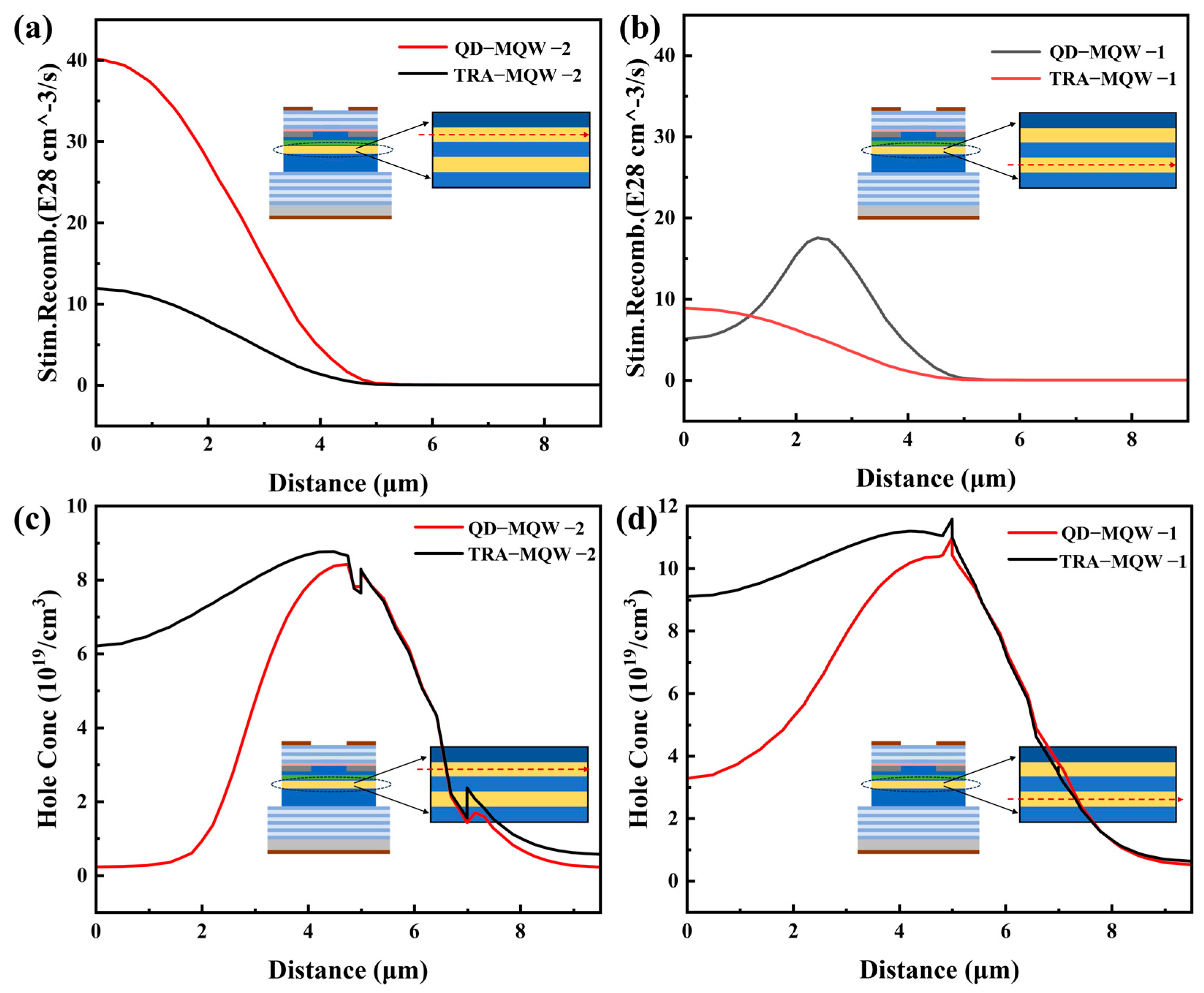
3.2. Recombination Analysis
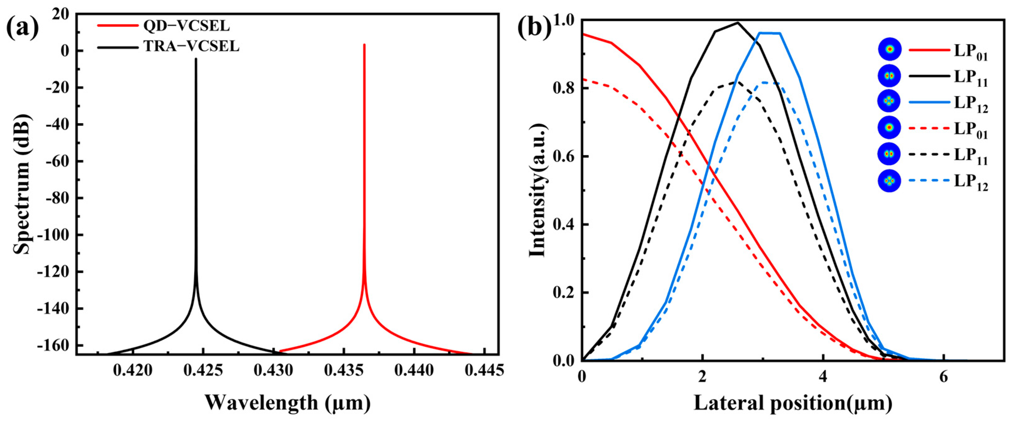
The carrier injection efficiency and the barrier height affect IQE. Figure 4a,b show the distribution of the electron and hole wavefunctions in the quantum wells. The electron and hole wavefunctions normalized to the wavefunctions are calculated, and the wavefunction overlap Γ is the ratio of the green area to the total area of the curve integral. The Γ of the QD-VCSEL is 46.3%, while the Γ of the TRA-VCSEL is 35.9%, which shows that the addition of the QD-embedded structure increases the Γ by 10.4%, which in turn enhances the IQE [35]. The IQE of QD-VCSEL is calculated to be 50.2%, while that of TRA-VCSEL is only 27.6%, and the IQE of QD-VCSEL is increased by 22.6% compared with that of TRA-VCSEL. The reason for this is that QD-VCSEL can eliminate part of the piezoelectric polarization effect and attenuate the quantum-confined Stark effect in the active region [36], which can reduce the tilt of the energy band and enhance IQE, and the localization effect of the QDs also enhances the efficiency of radiative recombination and reduces the efficiency of nonradiative recombination, which enhances power and reduces the threshold current.
The improved carrier injection efficiency and wave function overlap-enhanced IQE can enhance the stimulated recombination efficiency and reduce the radiative recombination efficiency. Figure 4c,d show that the radiative recombination of QD-VCSEL is much lower than that of TRA-VCSEL. Meanwhile, the stimulated recombination efficiency is lower for QD-VCSEL than for TRA-VCSEL in MQW-1, and the stimulated recombination efficiency of QD-VCSEL is more than twice as high as that of TRA-VCSEL in MQW-2. From Figure 4c,d, it can be seen that the efficiency of both radiative recombination and stimulated recombination in MQW-2 is higher than that in MQW-1; the reason for this is that the magnitude of the barrier height affects the carrier injection, and the electron and hole barriers in MQW-2 are lower than those in MQW-1. The carriers are more likely to be injected into MQW-2 to undergo the recombination, which suggests that MQW-2 is the main recombination center and that the QD-VCSEL is more than twice as efficient as the TRA-VCSEL. The increased stimulated recombination of the VCSEL can significantly increase the power and reduce the threshold current density. From Figure 4e,f, it can be seen that the recombination efficiency of QD-VCSEL is much lower than that of TRA-VCSEL, both for Auger recombination and SRH recombination, which suggests that the introduction of the embedded QDs can significantly reduce the Auger recombination and the SRH recombination. It is well known that the Auger effect is a three-particle effect. At the same time, Auger recombination is a process in which electrons and holes are directly recombined while transferring energy to another free carrier. Therefore, the low carrier concentration in the active region can effectively reduce the occurrence of Auger recombination. This situation also effectively reduces the occurrence of deep defects that trap electrons and holes as the recombination center without generating photons.
From Figure 5a, it can be seen that the stimulated recombination efficiency of the QD-VCSEL with MQW-2 is much higher than that of the TRA-VCSEL, enhanced stimulated recombination is a crucial factor contributing to the increased power, and the realization of strong efficiency in the stimulated recombination is necessary for obtaining high power. The transverse analysis shows that both Figure 5a,b show that the stimulated recombination efficiency drops to zero after a distance of 5 µm. This phenomenon can be attributed to the structural design featuring a precisely engineered 5 µm aperture, which effectively confines the region of stimulated recombination. The SiO2 layer completely blocks the surrounding area beyond this 5 µm boundary. Furthermore, the simulation results consistently validate the rationality of this structural design and the accuracy of the corresponding calculations. From Figure 5a, it can be seen that the efficiency of the transverse stimulated recombination of the QD-VCSEL is much stronger than that of the TRA-VCSEL in MQW-2. In Figure 5b, the stimulated recombination efficiency of the QD-VCSEL increases and then decreases because the stimulated recombination in MQW-2 accounts for the main index of the stimulated recombination, and most of the holes and electrons undergo stimulated recombination to produce photons in MQW-2. As the efficiency of the lateral distribution of the stimulated recombination in MQW-2 decreases, the holes and electrons migrate to MQW-1 for further stimulated emission, with the lateral distribution of MQW-2 stimulated recombination parameters declining. Then, the holes and electrons in MQW-2 can jump to MQW-1 for stimulated recombination. Figure 5a,b also present the TRA-VCSEL’s stimulated recombination, which is seen to be the main index of the stimulated recombination. The performance of TRA-VCSEL is worse than that of QD-VCSEL, proving the superiority of QD-embedded structures, which can substantially increase the efficiency of stimulated recombination.
From Figure 5c, it can be observed that as the excitation power increases, the hole concentration of both samples initially rises, reaching a peak value before gradually decreasing with further increases in excitation power. In contrast, the hole concentration of QD-VCSEL is much lower than that of TRA-VCSEL at the center of the aperture, mainly due to the high efficiency of the stimulated recombination. It can be seen that the efficiency of the stimulated recombination of QD-VCSEL is much higher than that of TRA-VCSEL, as shown in Figure 5a. The carriers are consumed in large quantities in MQW-2, which leads to the relatively low hole concentration at the center of the aperture. As the efficiency of stimulated recombination decreases, the hole concentration of both MQWs increases and reaches its peak at 5 μm before it starts to decrease, which also coincides with the design of the lateral optical confinement structure. The lateral optical confinement structure is designed to increase the hole concentration in the aperture, and the high hole density can promote power enhancement [37]. From Figure 5d, it can be seen that the hole concentration in the aperture center of the QD-VCSEL is one order of magnitude lower than that of the TRA-VCSEL because of the strongly stimulated radiation efficiency of the QD-VCSEL in both MQW-1 and MQW-2, which results in the hole concentrations in the center of the aperture being much lower than those seen for the TRA-VCSEL. According to the peak of stimulated recombination in MQW-2, the hole concentrations in MQW-2 also start to rise sharply after 2.1 µm, and the efficiency of stimulated recombination can correctly reflect the rise in hole concentration.
Based on the above discussion, it can be seen that the electron and hole concentrations of QD-VCSEL within the 5 µm oxide aperture are lower than those of TRA-VCSEL. The reason for is that QDs, as zero-dimensional materials, can contain both electrons and holes, substantially reducing the threshold current. The aforementioned analysis reveals that the quantum dot (QD) size effect contributes to a dual enhancement: it not only improves the internal quantum efficiency (IQE) but also, through the QD-embedded structure, promotes effective carrier localization within both the QD and quantum well regions. This structural configuration significantly reduces carrier escape probability from the active region while substantially improving carrier utilization efficiency, ultimately leading to a remarkable enhancement in optical power output.

3.3. Optical Mode

In order to provide strong transverse optical confinement, we added a light-guided structure with transverse optical confinement. According to previous studies, it is known that the total internal loss of a standard GaN-based VCSEL with an indium tin oxide electrode/SiO2 aperture is as high as 70 cm−1, which is due to the SiO2 aperture structure that leads to the anti-guiding structure, leading to the need to obtain a favorable light-guiding structure [38]. The device is set up with a transverse light-constrained structure. According to the effective refractive index model, the relative refractive index [39] difference, Δn/n, can be calculated by calculating the local resonance wavelength shifts in the center and peripheral regions of the VCSEL:
λ c λ P λ c = Δ λ λ c = Δ n n
where λc is the resonance wavelength of the center region and λP is the resonance wavelength of the peripheral region of the center. When λcλP is greater than 0, the device can obtain positive photoconduction, and after calculation, the Δn/n of this SiO2 buried structure is 0.029, which shows positive guidance. Then, we simulated the excitation spectra of QD-VCSEL and TRA-VCSEL at an injection current of 20 mA and assessed the one-dimensional efficiency distributions of the transverse modes of QD-VCSEL and TRA-VCSEL.
Achieving a single-longitudinal-mode output is one of the necessities for GaN-VCSELs, and we adjusted the longitudinal mode spacing by designing the cavity length and DBR refractive index and thickness so that only one longitudinal mode falls in the gain interval of the active region. From Figure 6a, it can be seen that the TRA-VCSEL achieves a single-longitudinal-mode output at 424 nm. In comparison, the QD-VCSEL can achieve a stable single-longitudinal-mode output at 436 nm owing to the difference in the content of the wrapper layer and the QD-embedded structure. The transverse loss of light and the overlapping of optical modes also affect the performance, and the dashed lines in Figure 6b show the base mode (LP01), the first-order transverse mode (LP11), and the second-order transverse mode (LP21) provided by the QD-VCSEL, while the solid lines show the transverse mode provided by the TRA-VCSEL. It was observed that both devices exhibit well-constrained optical modes within the aperture, and the difference is that the introduction of the QD-embedded structure causes the mode half-height widths of the fundamental mode (LP01), the first-order transverse mode (LP11), and the second-order transverse mode (LP21) to gradually decrease, which is mainly attributed to the SiO2 buried structure. With the use of the QD-embedded structure, although it causes the excitation wavelength to be red-shifted, the lateral constraints of light are enhanced, and the optical distribution of the QD-VCSEL is more concentrated than that of the TRA-VCSEL, meaning that the material gain of the QD-VCSEL can be superior with the same spatial distribution, and a low threshold current can be obtained.

4. Conclusions

By designing a novel InGaN QD-embedded structure, it is demonstrated that GaN-based VCSELs incorporating this design achieve enhanced stimulated recombination and high IQE, significantly reducing the threshold current while increasing output power. Specifically, the IQE is improved by 22.6%, and the efficiency of stimulated recombination is enhanced by 190%. The QD-VCSEL exhibits a threshold current of 4 mA and an output power of 4.4 mW at an injection current of 20 mA, representing a 63.6% reduction in threshold current and a 26.1% increase in output power. Moreover, hole utilization in the two quantum wells is improved by 65.2% and 84.4%, respectively. Regarding optical modes, the designed QD-VCSEL achieves single-longitudinal-mode output at 436 nm and demonstrates superior optical mode performance in transverse modes compared to the TRA-VCSEL. These results indicate that the QD-embedded structure mitigates the quantum-confined Stark effect in the active region and alleviates energy band bending caused by polarization effects. Additionally, it reduces the hole barrier height, thereby enhancing hole injection efficiency, improving quantum efficiency, and boosting output power.

Author Contributions

Conceptualization, Z.H. and H.D.; methodology, H.D.; software, Z.J.; validation, Z.J., W.J. and L.S.; formal analysis, H.D.; investigation, Z.H.; resources, Z.H.; data curation, Z.H.; writing—original draft preparation, Z.H.; writing—review and editing, Z.H. and H.D.; visualization, Z.J.; supervision, W.J.; project administration, H.D., Z.J., W.J., L.S. and B.X. funding acquisition, H.D. and B.X. All authors have read and agreed to the published version of the manuscript.

Funding

This work was supported by Shanxi-Zheda Institute of Advanced Materials and Chemical Engineering (2022SX-TD018, 2021SX-AT001, 2021SX-AT002 and 2021SX-AT003), the National Natural Science Foundation of China (61904120 and 21972103), and Shanxi “1331 project”.

Institutional Review Board Statement

Not applicable.

Informed Consent Statement

Not applicable.

Data Availability Statement

The data that support the findings of this study are available from the corresponding authors upon reasonable request.

Acknowledgments

We would like to acknowledge Crosslight corp. for providing the simulation software for this work. We would also like to and thank everyone who helped with this work.

Conflicts of Interest

The authors declare no conflicts of interest.

References

  1. Liu, A.; Wolf, P.; Lott, J.A.; Bimberg, D. Vertical-cavity surface-emitting lasers for data communication and sensing. Photonics Res. 2019, 7, 121–136. [Google Scholar] [CrossRef]
  2. Weigl, B.; Grabherr, M.; Jung, C.; Jager, R.; Reiner, G.; Michalzik, R.; Sowada, D.; Ebeling, K.J. High-performance oxide-confined GaAs VCSELs. IEEE J. Sel. Top. Quantum Electron. 1997, 3, 409–415. [Google Scholar] [CrossRef]
  3. Zhang, C.; ElAfandy, R.; Han, J. Distributed Bragg reflectors for GaN-based vertical-cavity surface-emitting lasers. Appl. Sci. 2019, 9, 1593. [Google Scholar] [CrossRef]
  4. Yu, H.-C.; Zheng, Z.-w.; Mei, Y.; Xu, R.-B.; Liu, J.-P.; Yang, H.; Zhang, B.-P.; Lu, T.-C.; Kuo, H.-C. Progress and prospects of GaN-based VCSEL from near UV to green emission. Prog. Quantum Electron. 2018, 57, 1–19. [Google Scholar] [CrossRef]
  5. Rambu, A.P.; Tiron, V.; Oniciuc, E.; Tascu, S. Spontaneous Polarization Reversal Induced by Proton Exchange in Z-Cut Lithium Niobate α-Phase Channel Waveguides. Materials 2021, 14, 7127. [Google Scholar] [CrossRef]
  6. Ahmad, A.; Strak, P.; Koronski, K.; Kempisty, P.; Sakowski, K.; Piechota, J.; Grzegory, I.; Wierzbicka, A.; Kryvyi, S.; Monroy, E. Critical evaluation of various spontaneous polarization models and induced electric fields in III-nitride multi-quantum wells. Materials 2021, 14, 4935. [Google Scholar] [CrossRef]
  7. Solís-Cisneros, H.I.; Hu, Y.; Camas-Anzueto, J.L.; Grajales-Coutiño, R.; Anwar, A.-R.; Martínez-Revuelta, R.; Hernández-de-León, H.R.; Hernández-Gutiérrez, C.A. theoretical and computational analysis of a wurtzite-AlGaN DUV-LED to mitigate quantum-confined Stark effect with a zincblende comparison considering Mg-and Be-doping. Nanomaterials 2022, 12, 4347. [Google Scholar] [CrossRef]
  8. Hautier, G.; Miglio, A.; Ceder, G.; Rignanese, G.-M.; Gonze, X. Identification and design principles of low hole effective mass p-type transparent conducting oxides. Nat. Commun. 2013, 4, 2292. [Google Scholar] [CrossRef]
  9. Binks, D.; Dawson, P.; Oliver, R.; Wallis, D. Cubic GaN and InGaN/GaN quantum wells. Appl. Phys. Rev. 2022, 9, 041309. [Google Scholar] [CrossRef]
  10. Wu, X.G.; Jing, Y.; Zhong, H. In Situ Fabricated Perovskite Quantum Dots: From Materials to Applications. Adv. Mater. 2024, 2412276. [Google Scholar] [CrossRef]
  11. Lin, Y.-S.; Ma, K.-J.; Hsu, C.; Feng, S.-W.; Cheng, Y.-C.; Liao, C.-C.; Yang, C.; Chou, C.-C.; Lee, C.-M.; Chyi, J.-I. Dependence of composition fluctuation on indium content in InGaN/GaN multiple quantum wells. Appl. Phys. Lett. 2000, 77, 2988–2990. [Google Scholar] [CrossRef]
  12. Yuan, H.; Chen, Y.; Lin, R.; Tan, D.; Zhang, J.; Wang, Y.; Gazit, E.; Ji, W.; Yang, R. Modified Stranski–Krastanov growth of amino acid arrays toward piezoelectric energy harvesting. ACS Appl. Mater. Interfaces 2022, 14, 46304–46312. [Google Scholar] [CrossRef] [PubMed]
  13. Barettin, D. State of the Art of Continuous and Atomistic Modeling of Electromechanical Properties of Semiconductor Quantum Dots. Nanomaterials 2023, 13, 1820. [Google Scholar] [CrossRef] [PubMed]
  14. Muziol, G.; Turski, H.; Siekacz, M.; Szkudlarek, K.; Janicki, L.; Baranowski, M.; Zolud, S.; Kudrawiec, R.; Suski, T.; Skierbiszewski, C. Beyond quantum efficiency limitations originating from the piezoelectric polarization in light-emitting devices. Acs Photonics 2019, 6, 1963–1971. [Google Scholar] [CrossRef]
  15. Jiang, K.; Sun, X.; Shi, Z.; Zang, H.; Ben, J.; Deng, H.-X.; Li, D. Quantum engineering of non-equilibrium efficient p-doping in ultra-wide band-gap nitrides. Light Sci. Appl. 2021, 10, 69. [Google Scholar] [CrossRef]
  16. Barettin, D.; Sakharov, A.V.; Tsatsulnikov, A.F.; Nikolaev, A.E.; Pecchia, A.; auf Der Maur, M.; Karpov, S.Y.; Cherkashin, N. Impact of local composition on the emission spectra of InGaN quantum-dot LEDs. Nanomaterials 2023, 13, 1367. [Google Scholar] [CrossRef]
  17. Abbas, M.; Xu, X.; Rauf, M.; Kyaw, A.K.K. A Comprehensive Review on Defects-Induced Voltage Losses and Strategies toward Highly Efficient and Stable Perovskite Solar Cells. In Proceedings of the Photonics, Rome, Italy, 10–14 November 2024; p. 87. [Google Scholar]
  18. Ji, L.; Su, Y.-K.; Chang, S. InGaN/GaN multi-quantum dot light-emitting diodes. Phys. Status Solidi C 2004, 1, 2405–2408. [Google Scholar] [CrossRef]
  19. Zhang, M.; Banerjee, A.; Lee, C.-S.; Hinckley, J.M.; Bhattacharya, P. A InGaN/GaN quantum dot green (λ = 524 nm) laser. Appl. Phys. Lett. 2011, 98, 221104. [Google Scholar] [CrossRef]
  20. Weng, G.; Mei, Y.; Liu, J.; Hofmann, W.; Ying, L.; Zhang, J.; Bu, Y.; Li, Z.; Yang, H.; Zhang, B. Low threshold continuous-wave lasing of yellow-green InGaN-QD vertical-cavity surface-emitting lasers. Opt. Express 2016, 24, 15546–15553. [Google Scholar] [CrossRef]
  21. Mei, Y.; Weng, G.-E.; Zhang, B.-P.; Liu, J.-P.; Hofmann, W.; Ying, L.-Y.; Zhang, J.-Y.; Li, Z.-C.; Yang, H.; Kuo, H.-C. Quantum dot vertical-cavity surface-emitting lasers covering the ‘green gap’. Light: Sci. Appl. 2017, 6, e16199. [Google Scholar] [CrossRef]
  22. Usman, M.; Munsif, M.; Mushtaq, U.; Anwar, A.-R.; Muhammad, N. Green gap in GaN-based light-emitting diodes: In perspective. Crit. Rev. Solid State Mater. Sci. 2021, 46, 450–467. [Google Scholar] [CrossRef]
  23. Yang, T.; Chen, Y.-H.; Wang, Y.-C.; Ou, W.; Ying, L.-Y.; Mei, Y.; Tian, A.-Q.; Liu, J.-P.; Guo, H.-C.; Zhang, B.-P. Green vertical-cavity surface-emitting lasers based on InGaN quantum dots and short cavity. Nano-Micro Lett. 2023, 15, 223. [Google Scholar] [CrossRef] [PubMed]
  24. Hsu, T.-C.; Teng, Y.-T.; Yeh, Y.-W.; Fan, X.; Chu, K.-H.; Lin, S.-H.; Yeh, K.-K.; Lee, P.-T.; Lin, Y.; Chen, Z. Perspectives on UVC LED: Its progress and application. In Proceedings of the Photonics, Vancouver, BC, Canada, 18–21 October 2021; p. 196. [Google Scholar]
  25. Song, J.; Luo, Z.; Liu, X.; Li, E.; Jiang, C.; Huang, Z.; Li, J.; Guo, X.; Ding, Z.; Wang, J. The study on structural and photoelectric properties of zincblende InGaN via first principles calculation. Crystals 2020, 10, 1159. [Google Scholar] [CrossRef]
  26. Xu, R.; Akiyama, H.; Zhang, B. Impacts of SiO2-Buried Structure on Performances of GaN-Based Vertical-Cavity Surface-Emitting Lasers. IEEE Trans. Electron Devices 2023, 70, 5701–5706. [Google Scholar] [CrossRef]
  27. Duzgol, O.; Kyritsis, G.; Zakhleniuk, N. Travelling-wave modelling of the modulation dynamic performance of wavelength-tunable laser diodes using the integrated VPI and PICS3D software. IET Optoelectron. 2017, 11, 66–72. [Google Scholar] [CrossRef]
  28. Ho, C.-H.; Speck, J.S.; Weisbuch, C.; Wu, Y.-R. Efficiency and forward voltage of blue and green lateral LEDs with V-shaped defects and random alloy fluctuation in quantum wells. Phys. Rev. Appl. 2022, 17, 014033. [Google Scholar] [CrossRef]
  29. Heikman, S.; Keller, S.; Wu, Y.; Speck, J.S.; DenBaars, S.P.; Mishra, U.K. Polarization effects in AlGaN/GaN and GaN/AlGaN/GaN heterostructures. J. Appl. Phys. 2003, 93, 10114–10118. [Google Scholar] [CrossRef]
  30. Sun, H.; Park, Y.J.; Li, K.-H.; Liu, X.; Detchprohm, T.; Zhang, X.; Dupuis, R.D.; Li, X. Nearly-zero valence band and large conduction band offset at BAlN/GaN heterointerface for optical and power device application. Appl. Surf. Sci. 2018, 458, 949–953. [Google Scholar] [CrossRef]
  31. Hsieh, F.-J.; Wang, W.-C. Full extraction methods to retrieve effective refractive index and parameters of a bianisotropic metamaterial based on material dispersion models. J. Appl. Phys. 2012, 112, 064907. [Google Scholar] [CrossRef]
  32. Ruiz, N.; Fernández, D.; Stanojević, L.; Ben, T.; Flores, S.; Braza, V.; Carro, A.G.; Luna, E.; Ulloa, J.M.; González, D. Suppressing the effect of the wetting layer through AlAs capping in InAs/GaAs QD structures for solar cells applications. Nanomaterials 2022, 12, 1368. [Google Scholar] [CrossRef]
  33. Althib, H. Effect of quantum barrier width and quantum resonant tunneling through InGaN/GaN parabolic quantum well-LED structure on LED efficiency. Results Phys. 2021, 22, 103943. [Google Scholar] [CrossRef]
  34. Kim, Y.-S.; Marsman, M.; Kresse, G.; Tran, F.; Blaha, P. Towards efficient band structure and effective mass calculations for III-V direct band-gap semiconductors. Phys. Rev. B—Condens. Matter Mater. Phys. 2010, 82, 205212. [Google Scholar] [CrossRef]
  35. Zhang, Y.; Li, Y.; Xin, X.; Wang, Y.; Guo, P.; Wang, R.; Wang, B.; Huang, W.; Sobrido, A.J.; Li, X. Internal quantum efficiency higher than 100% achieved by combining doping and quantum effects for photocatalytic overall water splitting. Nat. Energy 2023, 8, 504–514. [Google Scholar] [CrossRef]
  36. Baten, M.Z.; Alam, S.; Sikder, B.; Aziz, A. III-nitride light-emitting devices. Photonics 2021, 8, 430. [Google Scholar] [CrossRef]
  37. Zhao, L.; Liu, C.; Wang, K. Progress of GaN-Based Optoelectronic Devices Integrated with Optical Resonances. Small 2022, 18, 2106757. [Google Scholar] [CrossRef]
  38. Xu, R.; Mei, Y.; Xu, H.; Yang, T.; Ying, L.; Zheng, Z.; Long, H.; Zhang, B.; Liu, J. Effects of lateral optical confinement in GaN VCSELs with double dielectric DBRs. IEEE Photonics J. 2020, 12, 1–8. [Google Scholar] [CrossRef]
  39. Andreoli, F.; Gullans, M.J.; High, A.A.; Browaeys, A.; Chang, D.E. Maximum refractive index of an atomic medium. Phys. Rev. X 2021, 11, 011026. [Google Scholar] [CrossRef]
Figure 1. Traditional quantum well and quantum-well-embedded GaN QD VCSEL structures.
Photonics 12 00276 g001
Figure 2. (a) P-I image and (b) V-I image of both VCSELs.
Photonics 12 00276 g002
Figure 3. Energy band diagrams of (a) TRA-VCSEL and (b) QD-VCSEL in the [0001] direction at injection current 20 mA.
Photonics 12 00276 g003
Figure 4. (a) Electron–hole wave function distribution of TRA −VCSEL; (b) electron–hole wave function distribution of QD −VCSEL; (c) radiative recombination efficiency in the [0001] direction of TRA −VCSEL and QD −VCSEL; (d) stimulated recombination efficiency in the [0001] direction of TRA −VCSEL and QD −VCSEL; (e) Auger recombination efficiency in the [0001] direction of TRA −VCSEL and QD −VCSEL; (f) SRH recombination efficiency in the [0001] direction of TRA −VCSEL and QD −VCSEL.
Photonics 12 00276 g004
Figure 5. (a) Transverse stimulated recombination efficiency of MQW −2. (b) Transverse stimulated recombination efficiency of MQW −1. (c) Transverse hole concentrations of MQW −2. (d) Transverse hole concentrations of MQW −1.
Photonics 12 00276 g005
Figure 6. (a) Emission spectra of QD −VCSEL and TRA −VCSEL at an injection current of 20 mA and (b) transverse mode intensity distribution of QD −VCSEL and TRA −VCSEL.
Photonics 12 00276 g006
Table 1. Detailed structural parameters of VCSEL devices.
TypeMaterialThickness (nm)Doping Concentration (cm−3)
P-DBRTa2O5/SiO21556.4
Current spreading layerITO20
P-GaNGaN476p:4e23
EBLAl0.2Ga0.8N20p:1e24
MQWsIn0.16Ga0.84N/GaN(2.5/6) × 2 pairs
QDIn0.23Ga0.77N1
Layer wrapperIn0.16Ga0.84N0.75
N-GaNGaN1900n:2.5e24
N-DBRTa2O5/SiO21297
Table 2. Main parameter settings in the calculation.
ParameterValue
Auger recombination coefficient (m6/s)1.4 × 10−43
Lifetime (e/s)1 × 10−8
Polarizability %40
InGaN/GaN conduction band step/valence band step ratio70/30
AlGaN/GaN conduction band step/valence band step ratio50/50
Average optical loss outside active area (m−1)1000
Table 3. Detailed structural parameters of the quantum-well-embedded InGaN QD structure.
ParameterValue
Period (nm)10
Height (nm)1
Width (nm)2
GaN base layer wrapper (nm)6
In0.16Ga0.84N-well layer wrapper (nm)0.75
Disclaimer/Publisher’s Note: The statements, opinions and data contained in all publications are solely those of the individual author(s) and contributor(s) and not of MDPI and/or the editor(s). MDPI and/or the editor(s) disclaim responsibility for any injury to people or property resulting from any ideas, methods, instructions or products referred to in the content.

