Article

Pump-Probe Detection of Diamond Ionization and Ablation Induced by Ultra-Fast Laser

1
School of Electronics and Information Engineering, Hebei University of Technology, Tianjin 300131, China
2
Laboratory of All-Solid-State Light Sources, Institute of Semiconductors, Chinese Academy of Sciences, Beijing 100083, China
3
College of Science, Minzu University of China, Beijing 100081, China
4
Engineering Technology Research Center of All-Solid-State Lasers Advanced Manufacturing, Beijing 100083, China
5
College of Materials Science and Opto-Electronic Technology, University of Chinese Academy of Sciences, Beijing 101407, China
*
Author to whom correspondence should be addressed.
Photonics 2025, 12(3), 280; https://doi.org/10.3390/photonics12030280
Submission received: 14 February 2025 / Revised: 11 March 2025 / Accepted: 17 March 2025 / Published: 18 March 2025
(This article belongs to the Topic Laser-Induced Damage Properties of Optical Materials)

Abstract

:
Diamond, widely used in optoelectronic devices, plays a crucial role in improving performance through studies of its electronic structure and optoelectronic response. This study combines computational methods and experiments for analysis. Density functional theory calculates the diamond’s band structure and refractive index, while the Keldysh formula determines the laser intensity at the critical plasma density by evaluating laser-induced free electron density. By integrating the coupled model with a multi-physics field associative assignment, the critical plasma length in the diamond is further simulated. Experimentally, pump-probe techniques examine the diamond’s response under varying pulse widths and energies. Results show that increasing laser energy extends both plasma and damage lengths. As pulse width increases, plasma length first decreases and then increases, while graphitization length shows the opposite trend. Experiments show that laser energy enhancement significantly expands the plasma morphology by enhancing the nonlinear ionization effect. When the pulse width exceeds the electron-lattice relaxation time, the lattice energy deposition triggers localized graphitization, which enhances the subsequent laser absorption, and the final plasma distribution shows a high spatial correlation with the graphitized regions.

1. Introduction

Diamond, as a third-generation ultra-wideband semiconductor material, exhibits a face-centered cubic crystal structure. It possesses extremely high hardness (Mohs hardness 10), excellent thermal conductivity, and a low coefficient of thermal expansion. These properties endow it with great application potential in fields such as electronic and semiconductor devices [1,2], high-performance optical and electronic devices [3,4], and so on [5,6]. Diamond substrates used in the manufacturing of optical devices are generally divided into two categories: single-crystalline diamond and polycrystalline diamond. Due to its perfect crystal structure, single-crystalline diamond is widely used in high-power lasers and high-frequency electronic equipment [7]. Polycrystalline diamond is more suitable for large-scale production because of its lower cost [8]. Laser processing technology is a non-contact precision processing method featuring simplicity, high efficiency, flexibility, and environmental friendliness. Given its high precision and the ability to avoid material fracture and thermal damage that may be caused by traditional mechanical processing, this technology is widely applied in the drilling, cutting, and precision processing of hard and brittle materials [9,10].
In 2021, Wang et al. [11] used ultraviolet nanosecond laser and infrared picosecond laser to create microgrooves on the surface of the single-crystalline diamond and simulated the temperature distribution on the diamond surface under different laser pulses. This research revealed the material removal mechanism of diamonds during nanosecond and picosecond laser ablation. In 2022, Maxim et al. [12], for the first time, achieved laser polishing of diamond plates using femtosecond and nanosecond pulses, reducing the surface roughness from 5 μm to 1 μm. Zhai et al. [13] discovered that picosecond laser treatment caused significant material vaporization with minimal residue accumulation in processed areas when various microstructures were created on the surface of the chemical vapor deposition diamond. Graphitization occurred primarily in the grooves, with limited formation at the edges. In 2024, Cui et al. [14] studied nanosecond laser with the wavelength of 532 nm graphitization mechanisms in polycrystalline diamond. Molecular dynamics simulations showed that after 65 ps of laser irradiation followed by 25–45 ps energy diffusion, polycrystalline diamond first transformed into disordered amorphous carbon, followed by material removal and graphitization. Wang et al. [15] explored the dynamics of high-repetition-rate femtosecond laser-induced graphitization. Unlike low-repetition-rate scenarios, graphitization regions grew both towards and along the laser beam direction. Multiple surface scans reduced line thickness fluctuations, but continuous internal graphitization lines could not be formed via multi-scanning. Instead, comb-like structures developed through four distinct growth stages.
During ultra-short pulse laser processing, high-power density laser pulses can quickly initiate the generation of plasma on the material surface. For hard and brittle materials like diamonds, the interaction between the laser and the material leads to local heating and instantaneous evaporation of the material [16,17]. These shock waves enhance material removal efficiency while improving processing precision and depth control. Exploring the plasma dynamics within diamonds during laser processing is crucial for optimizing the process. Pump-probe technology, as a commonly used and effective time-domain resolution measurement method, plays an important role in related research [18,19]. In a pump-probe experiment, a short-pulse laser serves as the pump light to excite electrons, atoms, or molecules in the sample, generating plasma during laser-sample interaction. The probe light, also a short-pulse laser, is emitted after a controlled time delay following the pump light. By adjusting this delay, the time evolution of the sample after excitation can be observed.
In 2022, Itsuki et al. [20] used the dual pump-probe technique with femtosecond pulses and polarized pump pulses to conduct transient transmission change measurements and study the phonon interference phenomenon in diamonds. By using orthogonally polarized pulses, they observed the enhancement or suppression effect of the phonon amplitude. Orit et al. [21] studied the substitution, aggregation, and clustering behaviors of nitrogen impurities in diamonds and explored the different aggregation and clustering effects triggered by the substitution of carbon atoms by nitrogen atoms in the diamond crystal structure. Franky et al. [22] used ultrafast electron diffraction technology to study the structural changes in diamonds after laser excitation. With this technology, they tracked the dynamic changes in the diamond lattice and further explored the influence of laser heating on the crystal structure. Kai et al. [23] combined the pump-probe technology to study the photo-carrier dynamics of ZrTe3 under pressure and observed a significant laser heating effect, manifested as obvious changes in the contour and extension time of the echo period when the pump light intensity increased. However, traditional models mainly rely on single physical field approximations, and no coupled model with multi-physics field associative assignment has been reported for diamonds. Further analysis and research are needed regarding the influence of plasma concentration and morphological evolution through laser energy and pulse width.
In this study, a pulsed laser with a tunable pulse width ranging from 400 fs to 10 ps and a wavelength of 1040 nm was used for processing observation. Simulation of laser-induced plasma length inside a diamond was performed by using a coupled model with multi-physics field associative assignment, combining density functional theory (DFT), the Keldysh formula, and the finite element method. In the experiments, by changing parameters such as the pulse number, energy, and pulse width, the plasma morphology inside the diamond and the graphitized area were analyzed. Finally, the results obtained from the simulation model were close to those of the experimental measurements.

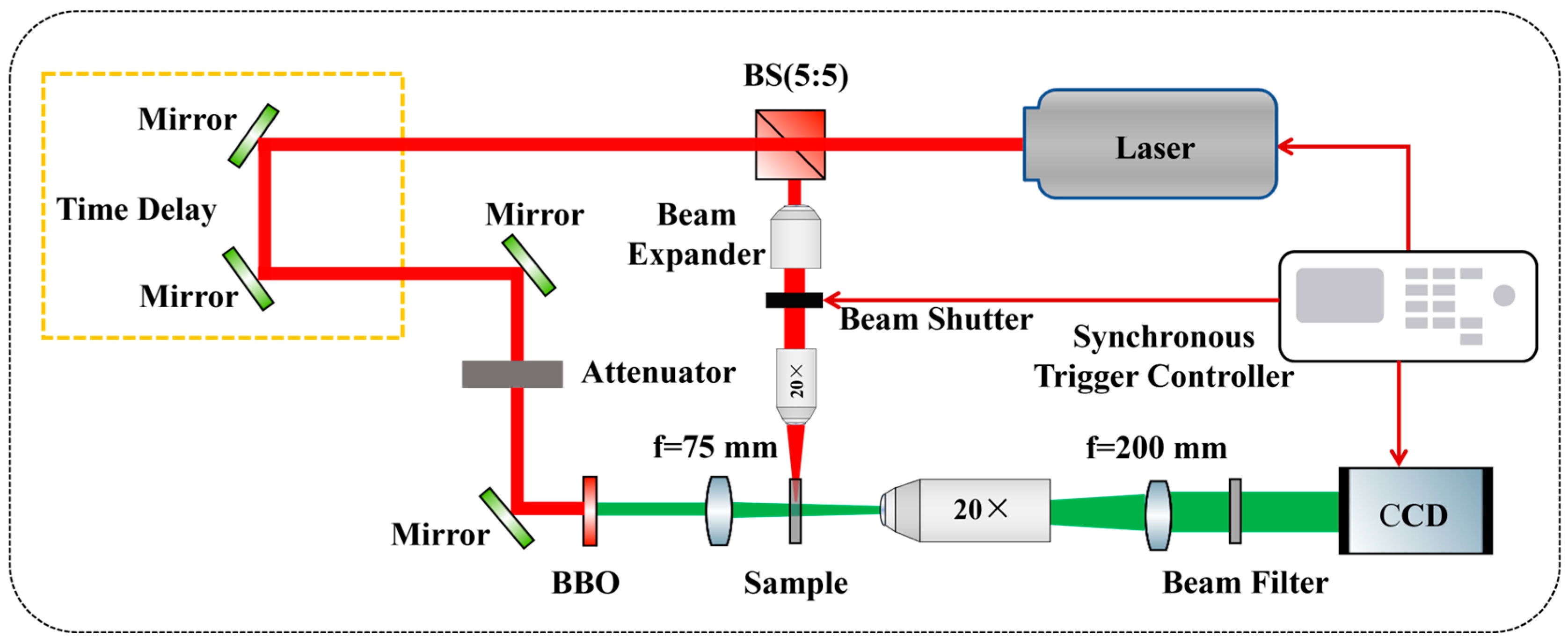
2. Materials and Methods

The diamond material used in the experiments is synthetic monocrystalline diamond, which is widely utilized in diamond machining tools. The sample is a square with the size of 5 mm × 5 mm × 2.5 mm. In the experiments, the femtosecond pulsed laser has a wavelength of 1040 nm (Spirit HE 1040-30, Spectra Physics, Milpitas, CA, USA), a pulse width ranging from 400 fs to 10 ps, and a repetition frequency of 10 Hz. As shown in Figure 1, after the laser is emitted, it is split into two beams of equal energy using a beam splitter. One beam is focused inside the material through an objective lens, serving as the processing laser. The other beam passes through a delay model and an optical attenuator before reaching a BBO crystal, generating a 532 nm wavelength laser that penetrates the material for detection. The final detection image is captured using a CCD camera (MV-GE2000C/M, MindVision, Shenzhen, China). The TTL signal generated by the laser is modulated by a Synchronous Trigger Controller (FY6900, FeelElec, Zhengzhou, China) and input into both the CCD and beam shutter, effectively controlling the number of pulses. The experimental results are observed and measured using a metallurgical microscope (Axio Scope A1, ZEISS, Baden-Württemberg, Germany). The reflectance and transmittance of the diamond were measured using a UV/visible/near-infrared spectrophotometer (Cary7000 UV–Vis–NIR, Agilent, Santa Clara, CA, USA), with results shown in Figure 2. At a wavelength of 1040 nm, the reflectance is 0.28, and the transmittance is 0.72. These values provide parameters for the subsequent numerical model development. The processing beam is focused by an objective lens with the numerical aperture NA = 0.4 (LMH −20×−1064, Thorlabs, Newton, NJ, USA), and the detection beam is focused by an objective lens with NA = 0.45 (M Plan Apo NIR 20×, Mitutoyo, Kanagawa, Japan).
The diameter of the focused beam spot is calculated using the formula 2 ω 0 = 1.83 λ 2 N A , where ω0 is the radius of the focused spot and λ is the laser wavelength. Thus, the calculated diameter of the focused spot 0 is 2.38 μm.

3. Results and Discussions

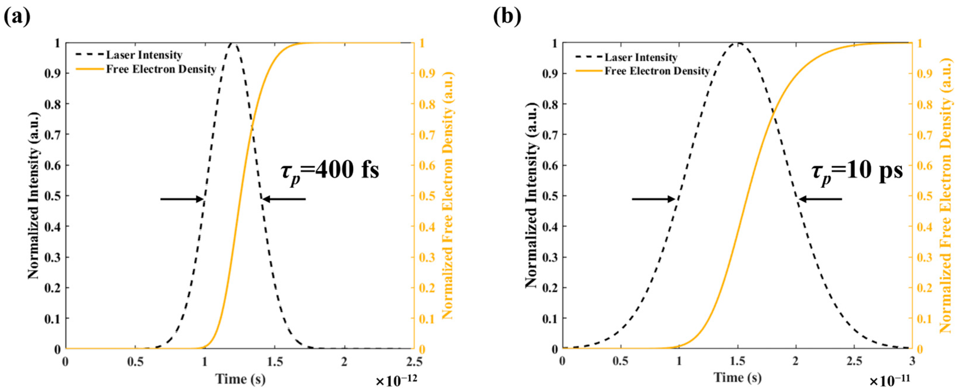
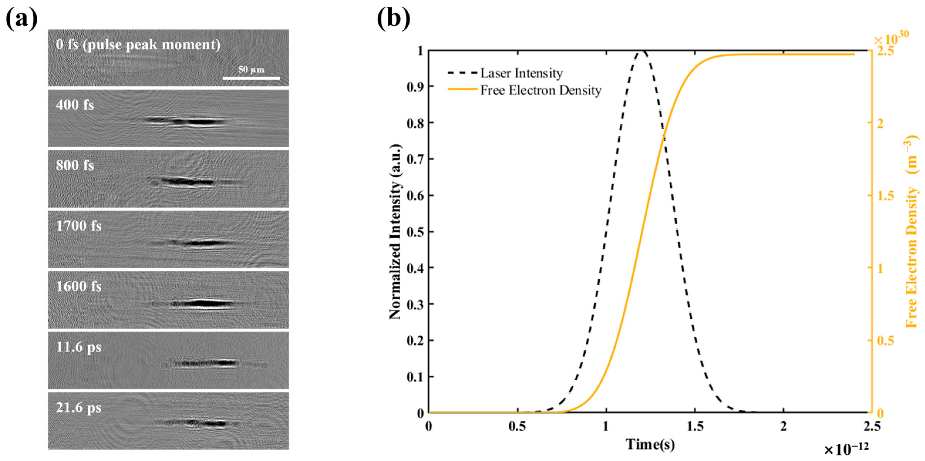
3.1. Multi-Physics Field Coupling Calculations

3.1.1. Density Functional Theory

Density functional theory (DFT) is a method based on electron density rather than the wave function. It is used to obtain the energy and electronic states of a system through the Kohn–Sham equations [24]:
ħ 2 2 m 2 + V e f f r ψ i r = ϵ i ψ i r
here, the wave function ψ i r represents the i-th electronic state, while ϵ i corresponds to the energy eigenvalue of the wave function ψ i r , and V e f f r represents the effective potential. By calculating the energy at different K-points in the Brillouin zone, the material’s band structure can be obtained. This structure consists of a series of discrete energy levels, reflecting the energy of the electronic states at each corresponding K-point. Solving the material’s dynamic polarization response allows for the determination of its dielectric function at different wavelengths, which can then be used to calculate the material’s refractive index and extinction coefficient.
The space group of diamonds is Fd3̅m. In the diamond unit cell, there are 8 carbon atoms: 4 located at the corners of the unit cell and the other 4 located at the face centers, as shown in Figure 3a. The calculation results, shown in Figure 3b,c, indicate that the band gap is Eg = 4.126 eV, the refractive index is n = 2.42, and the extinction coefficient is k = 0. These results provide the basis for subsequent simulation calculations.

3.1.2. Keldysh Formula

The computational model in this study focuses on plasma dynamics under single-pulse laser irradiation. It is assumed that the process affecting the conduction band electron density Ne is characterized by a rate that varies with time. These rates are combined into a rate equation, as given in [25]:
N e t t = w P I I t + w A V I t N e t w R N e t , t
where, wPI, wAV, and wR represent the capture defect rates for photoionization, avalanche ionization, and electron relaxation, respectively. The initial condition is Ne (t = 0) = 0, where I(t) is the incident laser intensity with a Gaussian distribution, and τp is the pulse width.
I t = I 0 exp ln 2 t 2 τ p 2
When a diamond is irradiated by a laser pulse, the electron density undergoes a slow decay, with a lifetime of around 100 ps [26]. Since the duration of the time pulse is much shorter than the time required for defect formation and electron capture by these defects, the last term on the right-hand side of Equation (2), which is related to recombination processes (such as the capture of electrons by crystal defects), is neglected.
The photoionization rate wPI is calculated using the Keldysh formula, which is expressed as follows [27]:
w P I = 2 2 ω 9 π 1 + γ 2 γ m ω 3 2 Q K γ , Δ ω exp π Δ ω + 1 K ϕ E ϕ E θ
where, ω is the frequency of the incident laser, and γ is the Keldysh parameter, defined as:
γ = ω m Δ e E ( x , z )
where m = 0.5 me is the effective mass [28], me is the electron mass, Δ is the initial band gap, e is the electron charge, E ( x , z ) is the amplitude of the electric field of laser radiation. The relationship between laser intensity F and electric field intensity E ( x , z ) is [29]:
F = n ε 0 c 2 E x , z 2
where n = 2.42 is the refractive index, ε0 is the vacuum dielectric constant, and c is the speed of light. The expression for avalanche ionization is given by [30]:
w A V = σ Δ I t
where, σ is the cross-section, given by:
σ = e 2 c ε 0 n m τ C 1 + ω 2 τ C 2
where τC is the electron collision time.
The maximum electron density as a function of laser intensity in the range of 1 × 10¹⁵ W/m2 to 1 × 10¹⁸ W/m2 is plotted. Additionally, the free electron densities for pulse widths of τp = 400 fs and τp = 10 ps are calculated separately, as shown in Figure 4.
The critical electron density NCR is given by [31]:
N C R = 4 π 2 c 2 m e ε 0 λ 2 e 2 = 1.03 × 10 27 m 3
The result is represented by the green dashed line in Figure 4. It can be observed that when the laser intensity reaches a level capable of generating the critical plasma density, the free electron density increases sharply. This is because, at this point, the laser intensity is strong enough to excite most of the electrons in the material into free states, resulting in the formation of a high-density plasma. To ensure complete excitation of the plasma, detection experiments are conducted after the plasma is fully excited, thereby avoiding interference from any incomplete excitation in the experimental results.
In the time domain, we calculated free electron density for τp = 400 fs and τp = 10 ps, with the laser intensity precisely reaching the critical value required to excite the plasma. The results are shown in Figure 5. In the figure, the black dashed line represents the incident laser waveform intensity, and the yellow curve corresponds to the free electron density.
When τp = 400 fs, the laser intensity reaches its peak at t = 1.2 ps, and the normalized electron density begins to rise at t = 1.35 ps, reaching its maximum value at t = 1.76 ps. When τp = 10 ps, its peak is t = 15 ps, and the normalized electron density starts to increase at t = 21.3 ps, reaching its maximum value at t = 30 ps. The increase rate of the free electron density is significantly larger at τp = 400 fs than that at τp = 10 ps. Therefore, in subsequent experiments, the measurement of free electron density will begin near the peak of the laser intensity.

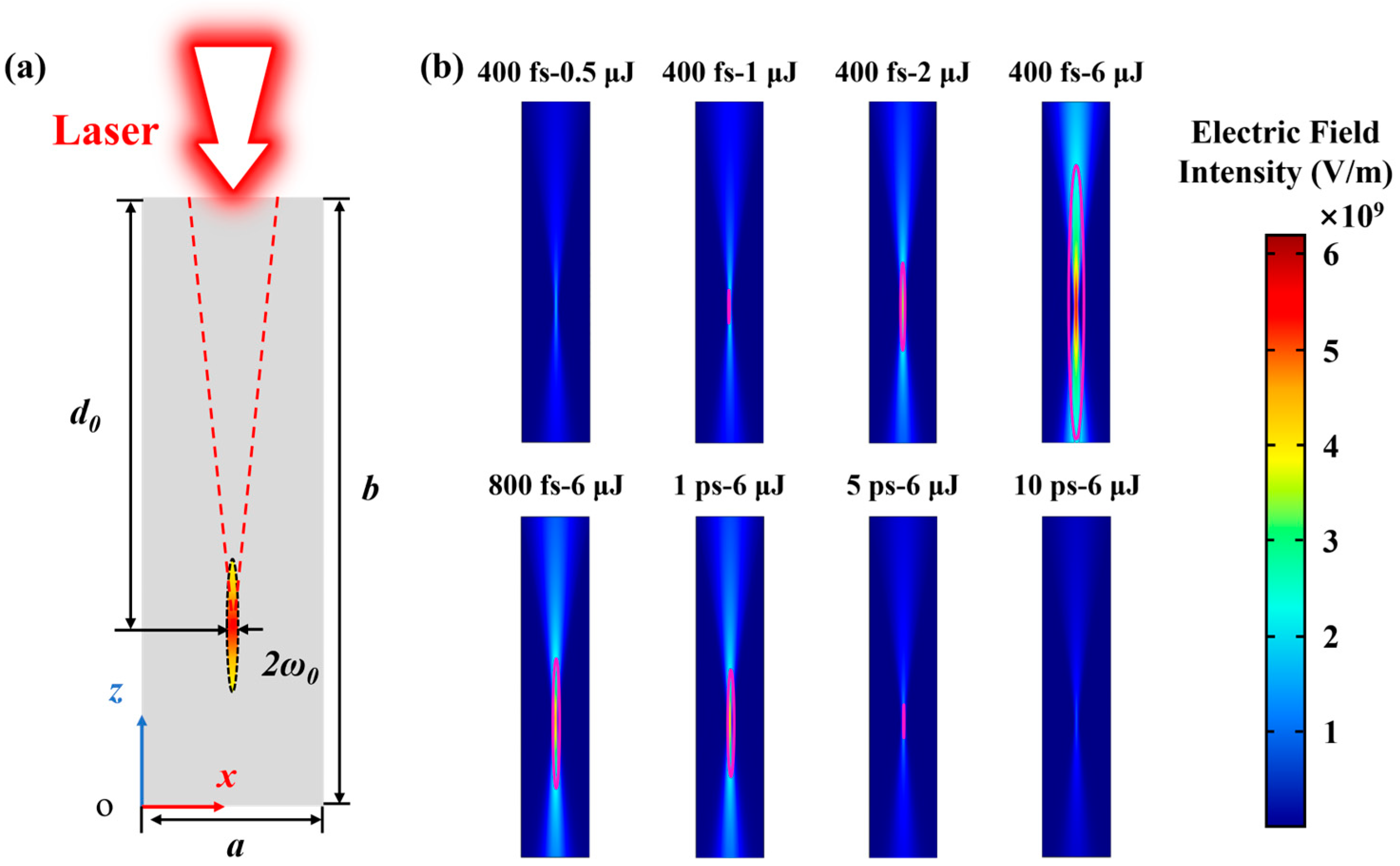
3.1.3. The Finite Element Method

To investigate the influence of pulse width τp and pulse energy F on the internal electric field distribution in diamond, a corresponding numerical model was established using the finite element method (FEM). As shown in Figure 6a, due to the difference in the refractive index, the focused laser spot formed inside the diamond exhibits a stretching phenomenon. In the model, the geometric dimensions of the diamond are a = 50 μm and b = 250 μm, with a focusing depth of d0 = 150 μm and a spot focus radius of ω0 = 1.19 μm. The laser wavelength is 1040 nm, incident along the -z direction. The numerical model is established under the following assumptions:
(1)
The spatial distribution of the incident laser follows a Gaussian beam profile.
(2)
The optical parameters of the diamond are treated as constants independent of laser intensity.
(3)
The free electron density evolution under an electric field is calculated via the Keldysh formula. The plasma generation threshold is defined as the electric field intensity at which the rate of plasma density increases dramatically.
(4)
The diamond material is an ideal conductor.
To ensure computational accuracy, the model employs a high-density mesh with a grid size of 0.01 μm, uniformly distributed within the calculation region. Based on the geometric structure and electromagnetic properties of diamond, the model discretizes the calculation domain and solves the electromagnetic field equations, thereby simulating the electric field distribution under different pulse width and pulse energy conditions. The electromagnetic field equations are as follows [32]:
E x , z = ω 0 ω x exp b z 2 ω x 2 exp i k 0 b z 2 2 R x + i η b z
where ω0, R, and η are the radius of the beam, wavefront curvature, and Gouy phase shift, respectively. The total electric field needs to be solved according to the Helmholtz equation:
2 + k 0 2 E t o t a l = 0 ; k 0 = 2 π λ
The incident field power is set as:
P = F τ p · ( 1 R 0 )
where R0 = 0.28 is the measured reflectance index.
The refractive index n of the material is 2.42, and the extinction coefficient k is set to 0. Both the incident surface and the exit surface are subject to scattering boundary conditions, and the initial electric field E(x, z) = 0.
The relationship between laser intensity and electric field amplitude can be derived from Equation (6). In the model described, a starting laser intensity is associated with a sudden change in electron density. The pump-probe system can instantaneously detect and capture this change. The corresponding electric field amplitude is then calculated and marked with a pink line on the electric field distribution. The area enclosed by the pink line is assumed to represent the plasma distribution that could be observed experimentally under these simulation conditions.
The results are displayed in Figure 6b. When τp = 400 fs, the plasma length increases gradually with increasing energy. However, when F = 6 μJ, the plasma length decreases as the pulse width increases. As the pulse energy increases, the laser intensity also rises, which makes it easier to excite electrons inside the material, leading to a stronger plasma formation. With higher pulse energy, electrons are more effectively heated and excited, resulting in a longer plasma length. When the pulse width increases, the energy transfer per unit time decreases, which reduces the laser intensity. For wider pulses, the instantaneous power is lower, making it unable to heat the material quickly in a short period of time. As a result, the electron temperature and energy generated by the laser pulse are insufficient to form a longer plasma.

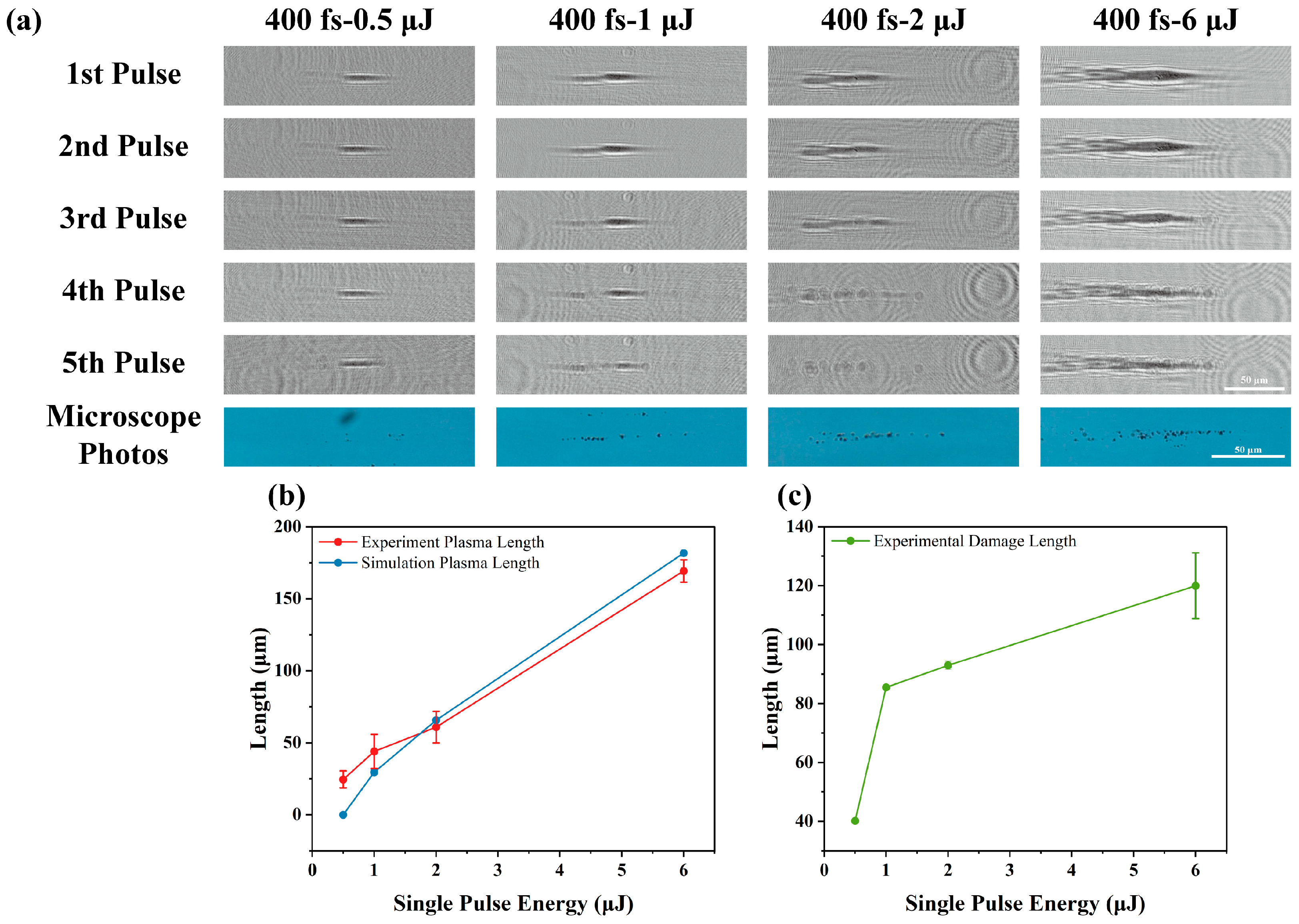
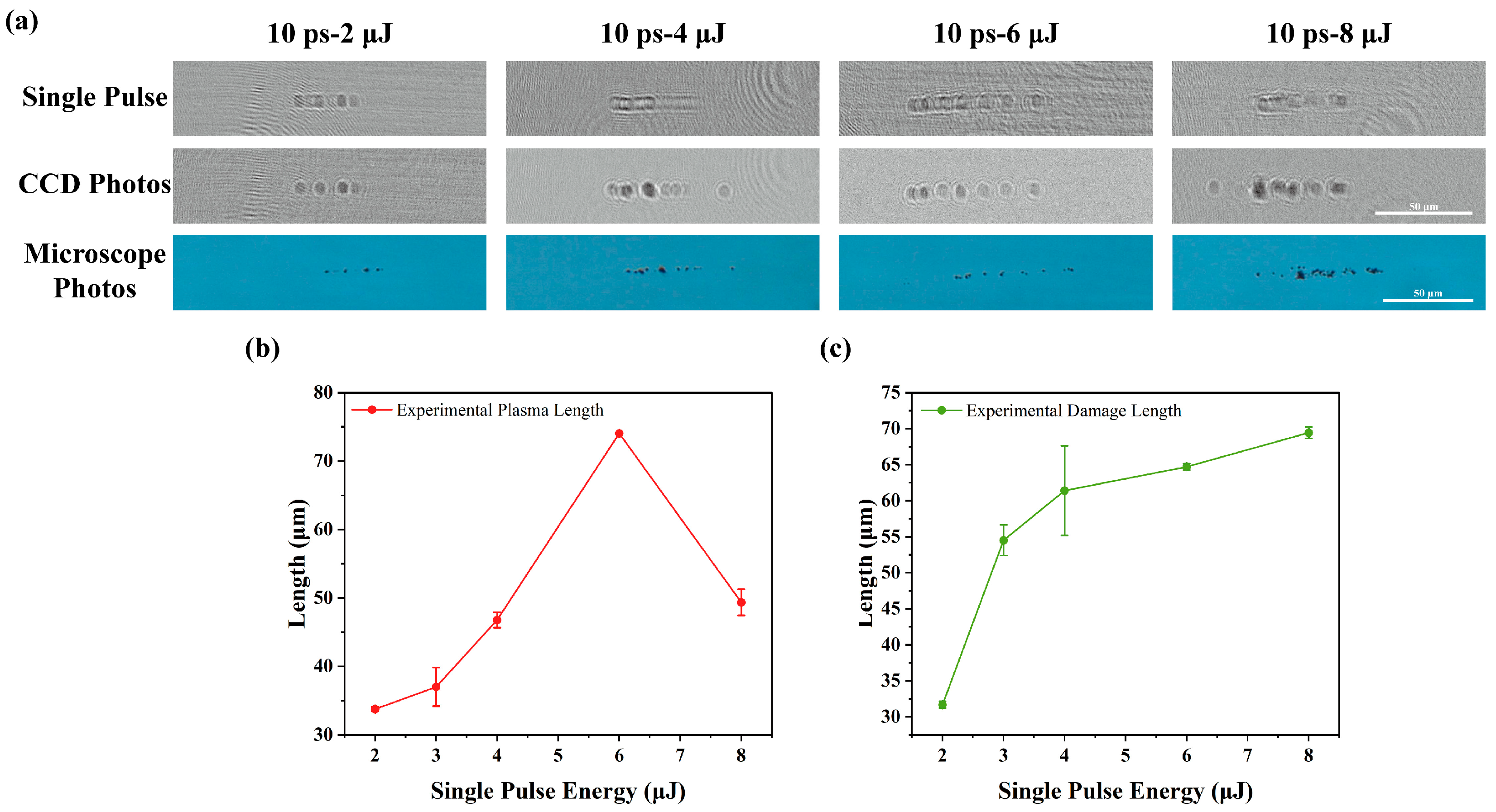
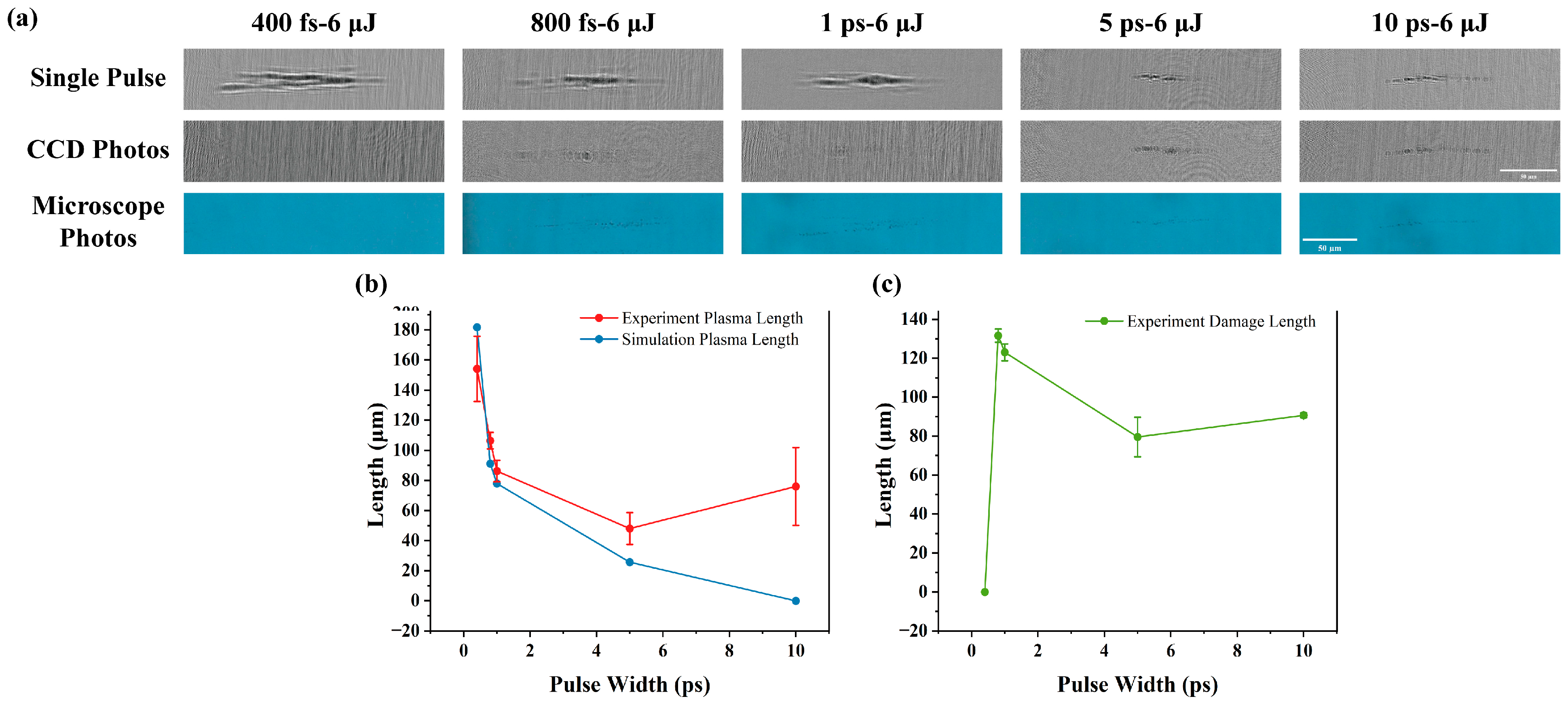
3.2. Experimental Results

In the experiments, a laser with τp = 400 fs and F = 2 μJ is focused at a depth of d0 = 150 μm inside the diamond for time-domain pump-probe measurements. As shown in Figure 7a, the laser had not yet been incident at 0 fs, but by 400 fs, plasma had already begun to form. At 800 fs, the free electron density had approached its maximum value. The experiment also found that the plasma decay process was relatively slow, with significant plasma signals still observable at 21.6 ps. Figure 7b shows the free electron density change obtained through numerical simulation under the same experimental conditions. As the laser intensity increased, the plasma generation time was advanced accordingly, and at around 400 fs from the pulse peak, the free electron density reached 2.48 × 1030 m−3, far exceeding the critical electron density.
Due to the extremely short duration of the laser pulse, the laser energy is rapidly absorbed and transferred to the electron system within such a short time. This causes the electrons to be excited to high energy states, resulting in plasma formation. The ultrafast laser-induced ionization and plasma formation occur on femtosecond timescales. However, since the laser pulse duration (τp = 400 fs) is orders of magnitude shorter than the decay time of electrons in the conduction band (about 140–190 ps [26]), the experimentally observed slow plasma density decay dynamics.
As shown in Figure 8, after varying the energy and laser pulse numbers at τp = 400 fs, graphite spots were observed in the sample after five pulses, and the distribution of these spots was consistent with the plasma morphology. The delay of the probe laser is 800 fs. When F = 0.5 μJ, almost no graphitization occurred. As the pulse energy increased, both the graphitization area and the plasma length gradually expanded. At the same time, the plasma length shown in the simulation results was consistent with the experimental plasma length generated by a single pulse.
When the laser intensity exceeds a certain threshold, the absorption characteristics of the diamond material change, leading to nonlinear interactions. Although the diamond itself has weak laser absorption, the laser can enhance energy absorption by exciting point defects and promoting inter-band transitions. As the laser pulse progresses, the diamond rapidly heats up, causing changes in its lattice structure and resulting in “thermal graphitization” [33].
When F = 0.5 μJ, the effect of the laser on the material is limited, leading to weak plasma generation and low energy transfer efficiency to the electron system and lattice. As a result, even after five pulses, only minimal damage is caused. However, as the laser pulse energy increases, the increase in peak power makes the plasma generation more intense. Higher energy more effectively heats the material, leading to structural changes within the material and facilitating the occurrence of graphitization. In addition, higher energies promote the earlier generation of graphitization, while the accumulation of pulses can continue to promote the growth of graphite uptake.
Experiments are conducted by increasing the pulse width to 10 ps and varying the energy, and the delay of the probe laser is around 20 ps. As shown in Figure 9, at τp = 10 ps, even with relatively low laser intensity, graphite shadows and plasma mixing are still observed, indicating that graphite is initially formed at this moment. This is because the pulse width is longer than the electron-lattice relaxation time (approximately 1 ps [34]). Therefore, the laser energy can be sufficiently conducted and redistributed within the material, allowing the diamond lattice to absorb energy, reach the graphitization temperature, and maintain high temperatures, thereby promoting graphitization [35]. As a result, the material can undergo graphitization even at lower power densities.
As the laser energy increases, the graphitization material damage length expands, and the plasma length first increases and then decreases. This behavior is due to the laser absorption by the already-formed graphite spots (since the linear absorption coefficient of graphite is orders of magnitude higher than that of diamond [36,37]). At F = 8 μJ, the initially ablated graphitized regions preferentially absorb subsequent laser energy, confining energy deposition to these regions rather than advancing deeper into the diamond. At high pulse energies, localized temperatures cause thermal diffusion to expand the phase transition zone outward from the ablation center. This process enlarges the graphitization area.
To further investigate the impact of pulse width, the laser energy F = 6 μJ was kept while the pulse width was varied in Figure 10. The results show that the plasma length generally decreases as the pulse width increases. It is noted that, at τp = 10 ps, graphite shadows are more pronounced relative to plasma.
A single pulse damage length first increases and then decreases, confirming that longer interactions between the laser and diamond promote graphitization. A longer pulse width provides more time for energy accumulation, which is beneficial for the reaction. However, an increase in pulse width reduces the energy injection per unit time, which weakens the nonlinear effects and makes it difficult to maintain the plasma for an extended period, leading to a decrease in the graphitization damage width. In contrast, with τp = 400 fs, the interaction time is extremely short, and the energy absorption and heating are highly concentrated. The electron-lattice coupling is negligible, and part of the energy cannot be converted into the heat required for graphitization. As a result, the material undergoes rapid heating and cooling, which is not conducive to the sustained graphitization reaction.

4. Conclusions

In summary, a coupled model with a multi-physics field associative assignment, combining DFT, the Keldysh formula, and FEM, is employed. The pulse number, energy, and pulse width of the laser are varied in experiments to study and discuss the plasma length and the graphitization damage length inside the diamond. The conclusions are as follows:
(1)
By assigning values to multiple physical models simultaneously, the variation trends of free-electron density with laser intensity or time were simulated and calculated under the conditions of τp = 400 fs and 10 ps. Also, the electric-field distribution and the plasma length inside the diamond under different energies and pulse widths are obtained.
(2)
When τp = 10 ps and 400 fs, respectively, the laser energy was changed. The results showed that as the laser energy increased, the plasma length also increased. Moreover, when the laser energy exceeded a certain threshold, the temperature of the diamond increased rapidly, and the lattice structure changed, leading to graphitization.
(3)
When the energy was fixed and the pulse width was varied, it was found that the plasma length first decreased and then increased as the pulse width increased, while the length of graphitization damage first increased and then decreased. With the increase in pulse width, the interaction time between the laser and diamond becomes more extended, which is favorable for the lattice to absorb energy and for graphitization to occur. The graphite’s absorption of the laser is much larger than that of the diamond, which makes the morphology of the plasma nearly the same as that of the graphite damage. As the pulse width increases, the energy injection per unit time decreases, decreasing the damage length.

Author Contributions

Conceptualization, J.D. and S.Z.; methodology, J.D.; simulation, J.D. and Y.S.; validation, J.D., Y.S. and J.W.; formal analysis, J.D.; investigation, J.D. and J.W.; resources, S.Z. and X.L.; data curation, J.D., Y.S. and J.W.; writing—original draft preparation, J.D.; writing—review and editing, S.Z.; visualization, J.D.; supervision, Y.P. and X.L.; project administration, X.L.; funding acquisition, X.L and Y.P. All authors have read and agreed to the published version of the manuscript.

Funding

This work was financially supported by the National Key R&D Program of China (No.2022YFB3605800), the CAS Project for Young Scientists in Basic Research, Grant No. YSBR-065, National Natural Science Foundation of China (No.62225507, No. U2033211, No. 62175230, No. 62175232, No. 62275244, No. 61905063), Scientific Instrument Developing Project of the Chinese Academy of Sciences, Grant No. YJKYYQ20200001, Key Program of the Chinese Academy of Sciences (ZDBS-ZRKJZ-TLC018).

Institutional Review Board Statement

Not applicable.

Informed Consent Statement

Not applicable.

Data Availability Statement

The raw data supporting the conclusions of this article will be made available by the authors on request.

Conflicts of Interest

The authors declare no conflicts of interest.

References

  1. Kononenko, V.V.; Bukin, V.V.; Komlenok, M.S.; Zavedeev, E.V.; Kononenko, T.V.; Dezhkina, M.A.; Ratnikov, P.P.; Dolmatov, T.V.; Chizhov, P.A.; Ushakov, A.A.; et al. A Diamond Terahertz Large Aperture Photoconductive Antenna Biased by a Longitudinal Field. Photonics 2023, 10, 1169. [Google Scholar] [CrossRef]
  2. Vyatkin, S.; Danilov, P.; Smirnov, N.; Pomazkin, D.; Kuzmin, E.; Gorevoy, A.; Muratov, A.; Matyaev, I.; Kudryashov, S. Electron Paramagnetic Resonance Sensing of «Hidden» Atomistic and Cooperative Defects in Femtosecond Laser-Inscribed Photoluminescent Encoding Patterns in Diamond. Photonics 2023, 10, 979. [Google Scholar] [CrossRef]
  3. Su, J.; Yang, G.; Guo, D.; Li, M.; Zhu, N.; Wang, X. Multi-Physical Analysis and Optimization in Integrated Lithium Niobate Modulator Using Micro-Structured Electrodes. Photonics 2023, 10, 795. [Google Scholar] [CrossRef]
  4. Komlenok, M.S.; Kononenko, V.V.; Bolshakov, A.P.; Kurochitskiy, N.D.; Pasternak, D.G.; Ushakov, A.A.; Konov, V.I. CVD Encapsulation of Laser-Graphitized Electrodes in Diamond Electro-Optical Devices. Photonics 2024, 11, 10. [Google Scholar] [CrossRef]
  5. Xing, Z.; Liao, J.; Xu, Z.; Cheng, X.; Zhang, J. The Design of Highly Reflective All-Dielectric Metasurfaces Based on Diamond Resonators. Photonics 2024, 11, 1015. [Google Scholar] [CrossRef]
  6. Yang, G.; Lu, Y.; Wang, B.; Xia, Y.; Chen, H.; Song, H.; Yi, J.; Deng, L.; Wang, Y.; Li, H. Chemical Vapor Deposition of <110> Textured Diamond Film through Pre-Seeding by Diamond Nano-Sheets. Materials 2022, 15, 7776. [Google Scholar] [CrossRef]
  7. Ren, Z.; Ma, Y.; Yang, S.; Yu, X.; Zhang, J.; Su, K.; Zhang, J.; Wang, H.; Hao, Y. High frequency single crystalline diamond MOSFET with high temperature (300 °C) ALD grown Al2O3 dielectric. Results Phys. 2023, 49, 106517. [Google Scholar] [CrossRef]
  8. Miyake, T.; Nakagawa, H.; Masuzawa, T.; Yamada, T.; Nakano, T.; Takagi, K.; Aoki, T.; Mimura, H. Diamond Radiation Detector with Built-In Boron-Doped Neutron Converter Layer. Phys. Status Solidi A 2022, 219, 2100315. [Google Scholar] [CrossRef]
  9. Yao, Y.; Chen, Q.; Li, B.; Zhang, J.; Wang, R.; Bai, M.; Liang, R.; Ma, L.; Ma, T.; Zhang, J.; et al. Influence of crystal orientation and incident plane on n-type 4H-SiC wafer slicing by using picosecond laser. Opt. Laser Technol. 2025, 182 Pt B, 112174. [Google Scholar] [CrossRef]
  10. Sakamoto, K.; Tokunaga, D.; Itoh, S.; Hidai, H.; Matsusaka, S.; Omatsu, T.; Koyama, K.; Kim, S.; Morita, N. Laser slicing of a diamond at the {100} plane using an irradiation sequence that restricts crack propagation along the {111} plane. Diam. Relat. Mater. 2023, 136, 110045. [Google Scholar] [CrossRef]
  11. Wang, H.; Wen, Q.; Xu, X.; Lu, J.; Jiang, F.; Cui, C. Ablation characteristics and material removal mechanisms of a single-crystal diamond processed by nanosecond or picosecond lasers. Opt. Express 2021, 29, 22714–22731. [Google Scholar] [CrossRef] [PubMed]
  12. Komlenok, M.; Pashinin, V.; Sedov, V.; Konov, V. Femtosecond and nanosecond laser polishing of rough polycrystalline diamond. Laser Phys. 2022, 32, 084003. [Google Scholar] [CrossRef]
  13. Zhai, J.; Zhang, Q.; Zhu, Y. Picosecond laser ablation of polycrystalline CVD diamond. Opt. Laser Technol. 2022, 155, 108403. [Google Scholar] [CrossRef]
  14. Cui, X.; Zhang, C.; Li, G.; Song, C.; Qin, W.; Wang, T. Mechanisms Behind Graphitization Modification in Polycrystalline Diamond by Nanosecond Pulsed Laser. Materials 2024, 17, 6200. [Google Scholar] [CrossRef]
  15. Wang, H.; Liu, B.; Pang, D.; Hu, M. Study of the dynamics of the graphitization in diamond induced by high repetition rate fs laser. Opt. Commun. 2024, 565, 130639. [Google Scholar] [CrossRef]
  16. Wen, Q.; Wang, H.; Xu, X.; Lu, J.; Huang, H.; Jiang, F. Study on nanosecond laser-induced iron plasma reactive etching of single-crystal CVD diamond. Opt. Laser Technol. 2024, 177, 111071. [Google Scholar] [CrossRef]
  17. Kononenko, V.V. Modification of Diamond Surface by Femtosecond Laser Pulses. Photonics 2023, 10, 1077. [Google Scholar] [CrossRef]
  18. Kumar, R.R.; Geethika, B.R.; Verma, N.; Chaudhari, V.; Dave, J.; Joshi, H.C.; Thomas, J. Effect of ambient on the dynamics of re-deposition in the rear laser ablation of a thin film. Opt. Laser Technol. 2025, 181 Pt C, 111954. [Google Scholar] [CrossRef]
  19. Pflug, T.; Olbrich, M.; Horn, A. Electron dynamics in fused silica after strong field laser excitation detected by spectroscopic imaging pump-probe ellipsometry. Phys. Rev. B 2022, 106, 014307. [Google Scholar] [CrossRef]
  20. Takagi, I.; Kato, T.; Kayanuma, Y.; Nakamura, G.K. Interference of optical phonons in diamond studied using femtosecond pulses of polarized near-infrared light. Solid State Commun. 2022, 350, 114747. [Google Scholar] [CrossRef]
  21. Arad, N.O.; Shlomi, H.D.; Manukovsky, N.; Laster, E.; Kaminker, I. Nitrogen Substitutions Aggregation and Clustering in Diamonds as Revealed by High-Field Electron Paramagnetic Resonance. J. Am. Chem. Soc. 2024, 146, 5100–5107. [Google Scholar] [CrossRef]
  22. Bernal, F.; Riffe, J.E.; Devlin, W.S.; Hamel, S.; Lindsey, K.R.; Reid, A.H.; Mo, M.; Luo, D.; Kramer, P.; Shen, X. Response of fs-Laser-Irradiated Diamond by Ultrafast Electron Diffraction. J. Phys. Chem. C 2024, 128, 18651–18657. [Google Scholar] [CrossRef]
  23. Zhang, K.; Xie, J.F.; Yang, J.; Wang, T.; Su, F.; Wu, Y.; Fang, G. Extraordinary suppression of the laser heating effect in ZrTe3 under pressure revealed by ultrafast spectroscopy. Phys. Rev. B 2024, 109, 115130. [Google Scholar] [CrossRef]
  24. Kachan, E.; Tsaturyan, A.; Stoian, R.; Colombier, J.P. First-principles study of ultrafast bandgap dynamics in laser-excited -quartz. Eur. Phys. J. Spec. Top. 2023, 232, 2241–2245. [Google Scholar] [CrossRef]
  25. Jupé, M.; Jensen, L.; Melninkaitis, A.; Sirutkaitis, V.; Ristau, D. Calculations and experimental demonstration of multi-photon absorption governing fs laser-induced damage in titania. Opt. Express 2009, 17, 12269–12278. [Google Scholar] [CrossRef]
  26. Martin, P.; Guizard, S.; Daguzan, P.H.; Petite, G.; D’Oliveira, P.; Meynadier, P.; Perdrix, M. Subpicosecond study of carrier trapping dynamics in wide-band-gap crystals. Phys. Rev. B 1997, 55, 5799. [Google Scholar] [CrossRef]
  27. Keldysh, L.V. Ionization in the field of a strong electromagnetic wave. J. Exp. Theor. Phys. 1965, 20, 1307–1314. [Google Scholar]
  28. Kononenko, V.V.; Konov, V.I.; Gololobov, V.M.; Zavedeev, E.V. Propagation and absorption of high-intensity femtosecond laser radiation in diamond. Quantum Electron. 2014, 44, 1099. [Google Scholar] [CrossRef]
  29. Halliday, D.; Resnick, R.; Walker, J. Fundamentals of Physics; Wiley: Hoboken, NJ, USA, 2002. [Google Scholar]
  30. Ashkroft, N.W.; Mermin, N.D. Solid State Physics; Saunders College Publishing: New York, NY, USA, 1976. [Google Scholar]
  31. Takabe, H. The Physics of Laser Plasmas and Applications: Physics of Laser Matter Interaction; Springer: Cham, Switzerland, 2020; Volume 1. [Google Scholar]
  32. Song, Y.; Zhao, S.; He, H.; Liang, H.; Dai, Z.; Lin, X.; Zhang, G. Numerical Simulation and Experimental Investigation of ps Pulsed Laser Modification inside 4H-SiC Material. Photonics 2024, 11, 189. [Google Scholar] [CrossRef]
  33. Kononenko, V.V.; Gololobov, V.M.; Kononenko, T.V.; Konov, V.I. Photoinduced graphitization of diamond. Laser Phys. Lett. 2015, 12, 016101. [Google Scholar] [CrossRef]
  34. Choi, C.K.; Kwon, Y.H.; Krasinski, J.S.; Park, G.H.; Setlur, G.; Song, J.J.; Chang, Y.C. Ultrafast carrier dynamics in a highly excited GaN epilayer. Phys. Rev. B 2001, 63, 115315. [Google Scholar] [CrossRef]
  35. Chichkov, B.N.; Momma, C.; Nolte, S.; Alvensleben, F.; Tünnermann, A. Femtosecond, picosecond and nanosecond laser ablation of solids. Appl. Phys. A 1996, 63, 109–115. [Google Scholar] [CrossRef]
  36. Yin, J.; Chen, G.; Zhu, Z.; Jin, M.; Hu, B. Ablation mechanism investigation and ablation threshold prediction of single crystal diamond irradiated by femtosecond laser. Diam. Relat. Mater. 2021, 111, 108173. [Google Scholar] [CrossRef]
  37. Sucharita, S. Nanosecond laser ablation of graphite: A thermal model based simulation. J. Laser Appl. 2018, 30, 012008. [Google Scholar] [CrossRef]
Figure 1. Schematic diagram of the pump-probe experimental setup.
Photonics 12 00280 g001
Figure 2. Results of reflectance (red line) and transmittance (blue line) measurements of the diamond used in the experiment obtained using a spectrophotometer.
Photonics 12 00280 g002
Figure 3. (a) Schematic diagram of the diamond model. (b) The simulation results of band structure and bandgap Eg and (c) refractive index n and extinction coefficient k of diamond calculated using DFT.
Photonics 12 00280 g003
Figure 4. Variation in free electron density with laser intensity, calculated under the conditions of τp = 400 fs and τp = 10 ps.
Photonics 12 00280 g004
Figure 5. Variation in the free electron density with time, calculated for (a) τp = 400 fs and (b) τp = 10 ps.
Photonics 12 00280 g005
Figure 6. (a) Schematic of the two-dimensional model used in FEM to calculate the distribution of the electric field inside the diamond. (b) Calculation results of the electric field intensity distribution inside the diamond under laser irradiation. The pink line represents the electric field intensity corresponding to the start of free electron density with a sudden change in electron density.
Photonics 12 00280 g006
Figure 7. When τp = 400 fs and F = 2 μJ, (a) shows the pump-probe measurements of the plasma morphology inside the diamond as it evolves over time; (b) shows the plasma density variation with time inside the diamond calculated using the model under the same conditions.
Photonics 12 00280 g007
Figure 8. (a) When τp= 400 fs, the variation in plasma length with changes in pulse energy and pulse number is observed. The change in graphitization damage length with energy after five pulses is also measured. The plasma length of a single laser pulse and the damage length of five laser pulse change curves are plotted in (b,c), respectively.
Photonics 12 00280 g008
Figure 9. (a) When τp = 10 ps, the variation in plasma length with changes in pulse energy is observed. The change in graphitization damage length with energy after a single pulse is also measured. The change curves are plotted in (b,c).
Photonics 12 00280 g009
Figure 10. (a) When F = 6 μJ, the variation in plasma length with changes in pulse width is observed. The change in graphitization damage length after the single pulse is also measured. The change curves are plotted in (b,c).
Photonics 12 00280 g010
Disclaimer/Publisher’s Note: The statements, opinions and data contained in all publications are solely those of the individual author(s) and contributor(s) and not of MDPI and/or the editor(s). MDPI and/or the editor(s) disclaim responsibility for any injury to people or property resulting from any ideas, methods, instructions or products referred to in the content.

