Inverse Design of Wavelength-Selective Film Emitter for Solar Thermal Photovoltaic System


Abstract
1. Introduction
2. Model and Method
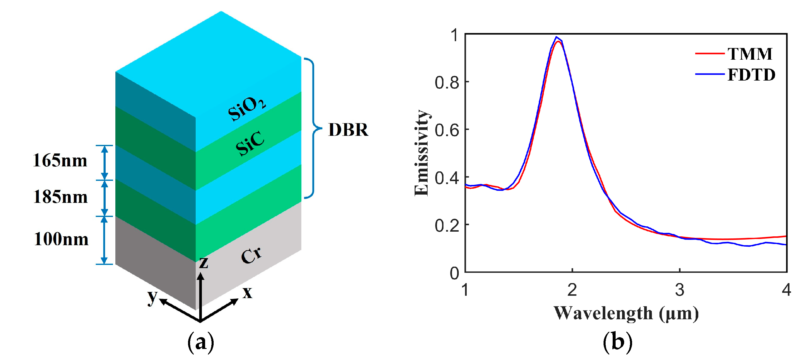
2.1. Target Spectra and Structure
2.2. Performance Evaluation
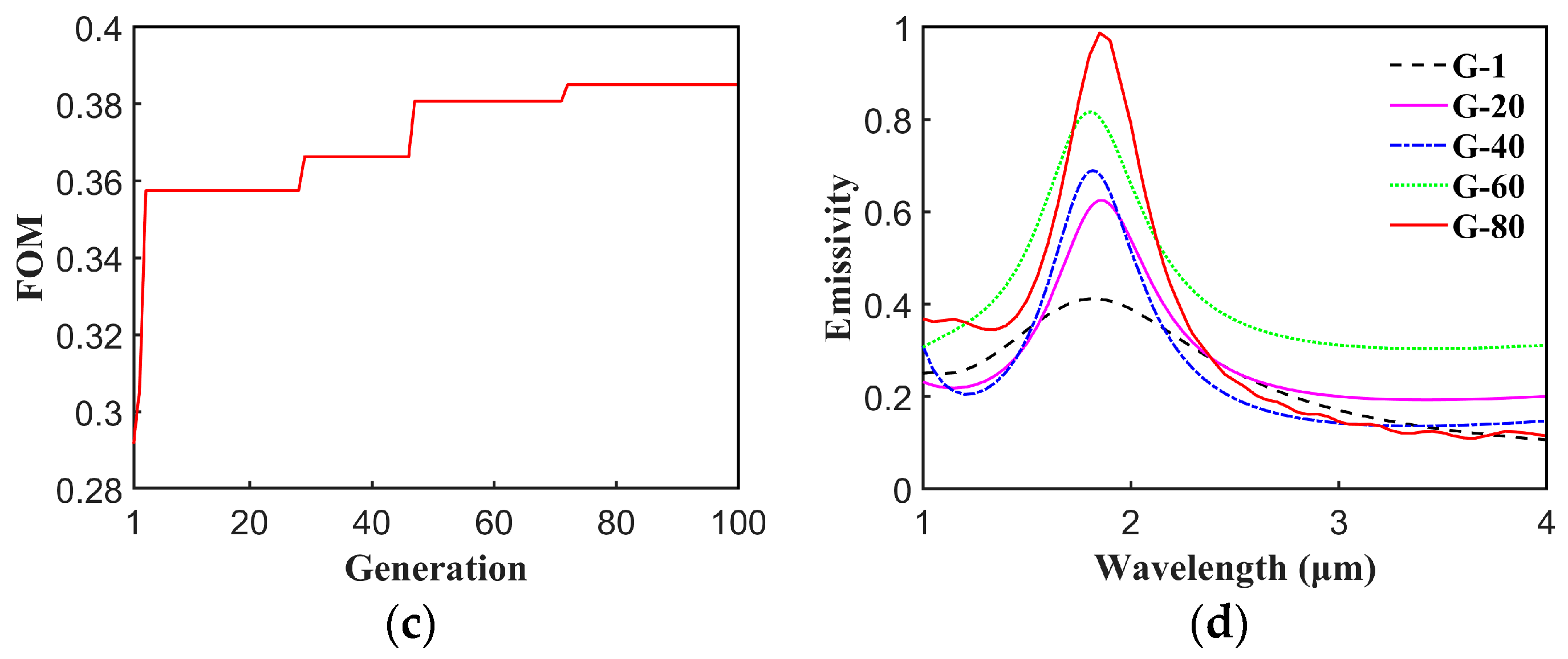
2.3. Inverse Design
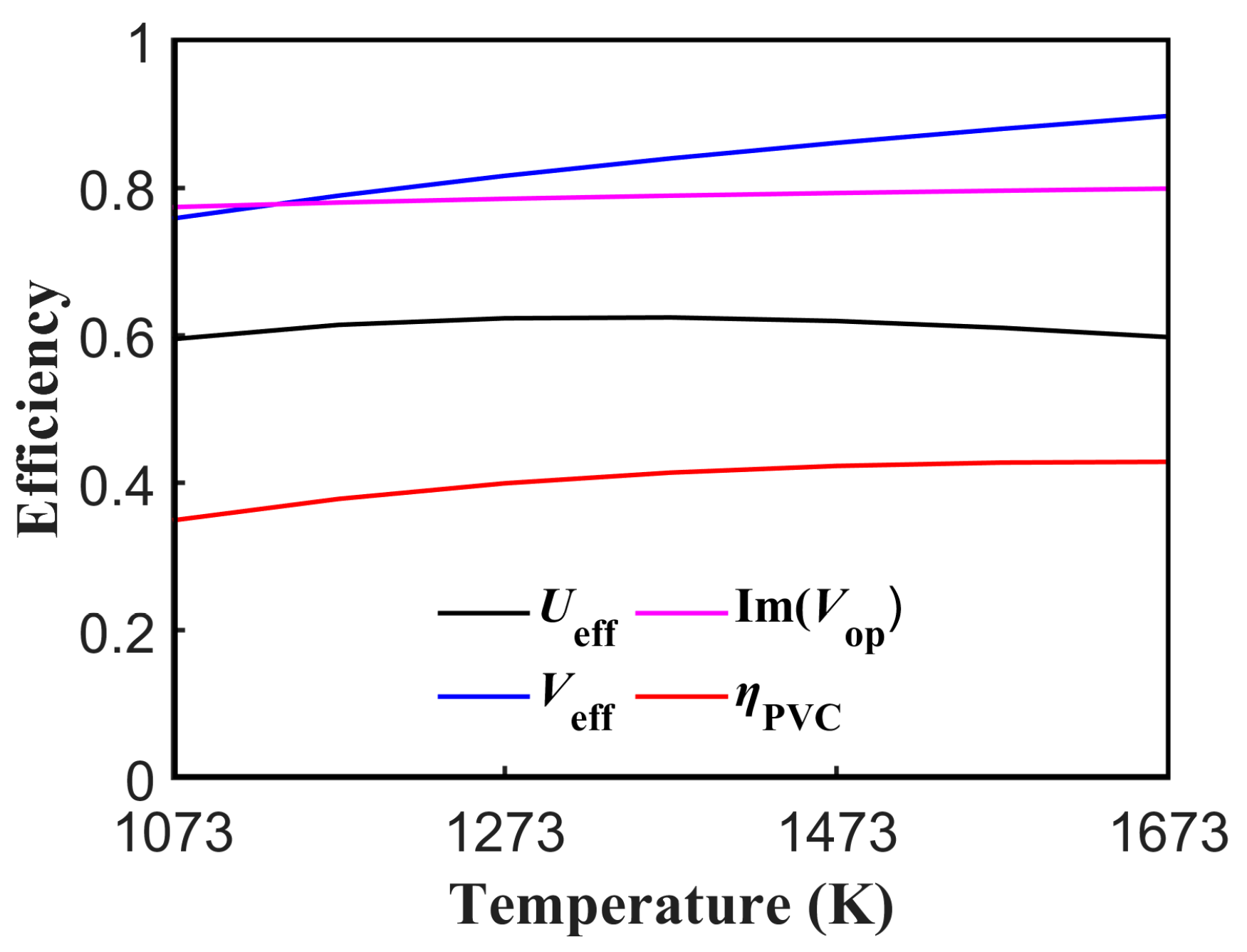
3. Results
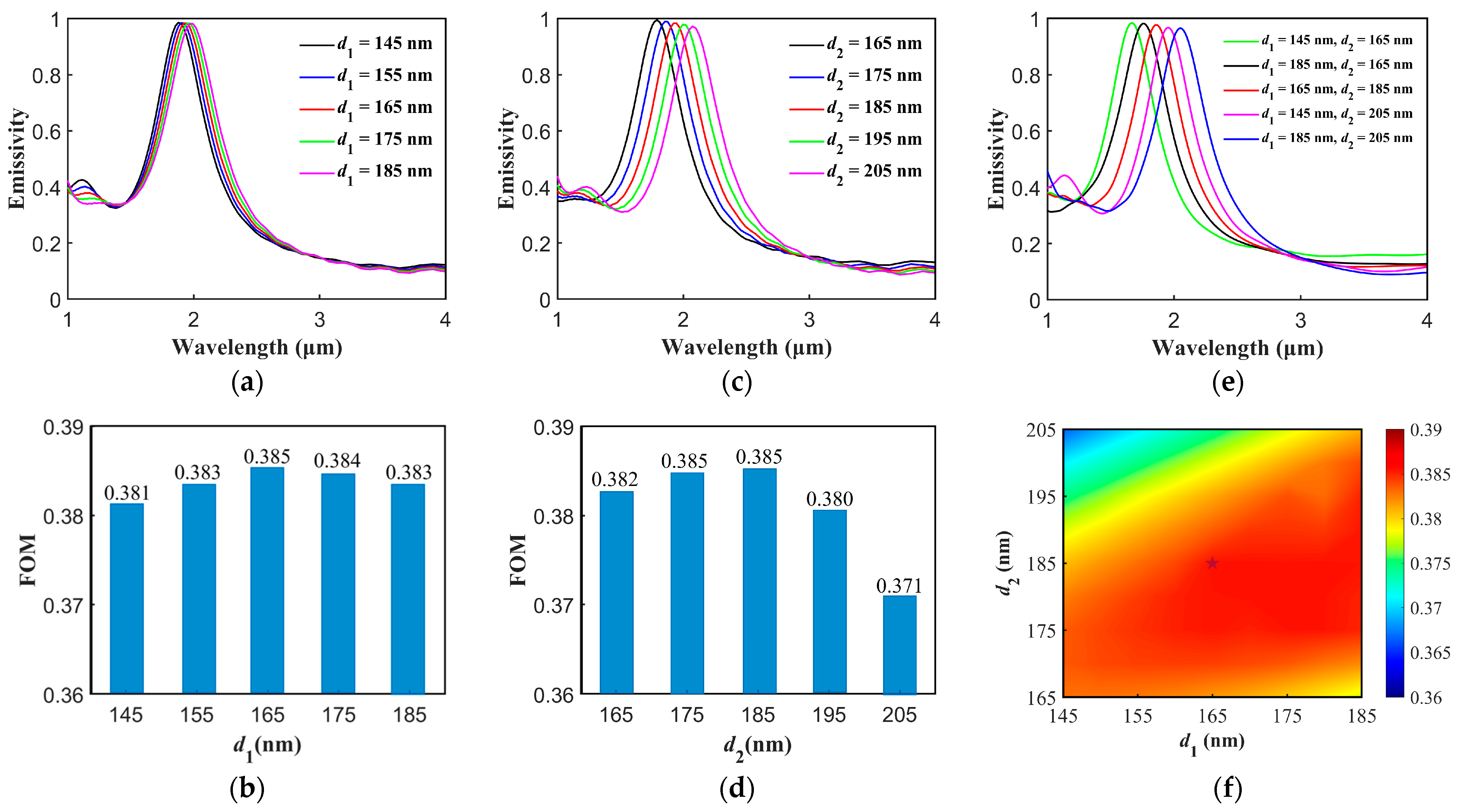
3.1. Results of Inverse Design
3.2. Electromagnetic Field and Robustness of the Structure
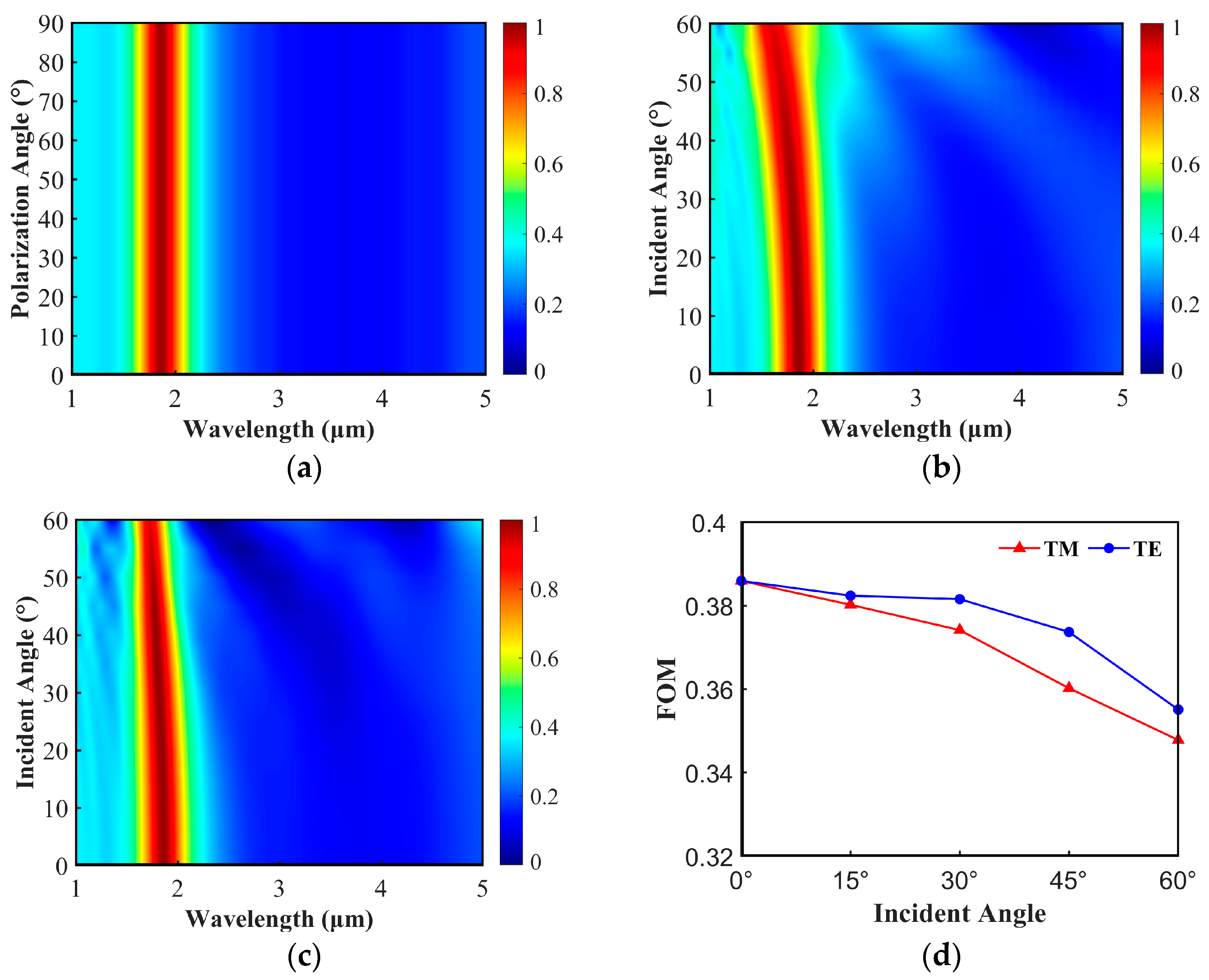
3.3. Angle Independence of the Emitter
4. Discussion
5. Conclusions
Supplementary Materials
Author Contributions
Funding
Institutional Review Board Statement
Informed Consent Statement
Data Availability Statement
Conflicts of Interest
References
- Hu, T.; Kwan, T.H.; Yang, H.; Wu, L.; Liu, W.; Wang, Q.; Pei, G. Photothermal Conversion Potential of Full-Band Solar Spectrum Based on Beam Splitting Technology in Concentrated Solar Thermal Utilization. Energy 2023, 268, 126763. [Google Scholar] [CrossRef]
- Xing, L.; Ha, Y.; Wang, R.; Li, Z. Recent Advances of Solar Thermal Conversion with Wide Absorption Spectrum Based on Plasmonic Nanofluids. Sol. Energy 2023, 262, 111858. [Google Scholar] [CrossRef]
- Moustakas, K.; Loizidou, M.; Rehan, M.; Nizami, A.S. A Review of Recent Developments in Renewable and Sustainable Energy Systems: Key Challenges and Future Perspective. Renew. Sustain. Energy Rev. 2020, 119, 109418. [Google Scholar] [CrossRef]
- Shockley, W.; Queisser, H.J. Detailed Balance Limit of Efficiency of p-n Junction Solar Cells. J. Appl. Phys. 1961, 32, 510. [Google Scholar] [CrossRef]
- Lenert, A.; Bierman, D.M.; Nam, Y.; Chan, W.R.; Celanović, I.; Soljačić, M.; Wang, E.N. A Nanophotonic Solar Thermophotovoltaic Device. Nat. Nanotechnol. 2014, 9, 126–130. [Google Scholar] [CrossRef]
- Rephaeli, E.; Fan, S. Absorber and Emitter for Solar Thermo-Photovoltaic Systems to Achieve Efficiency Exceeding the Shockley-Queisser Limit. Opt. Express 2009, 17, 15145. [Google Scholar] [CrossRef] [PubMed]
- Wang, H.; Chang, J.-Y.; Yang, Y.; Wang, L. Performance Analysis of Solar Thermophotovoltaic Conversion Enhanced by Selective Metamaterial Absorbers and Emitters. Int. J. Heat Mass Transf. 2016, 98, 788–798. [Google Scholar] [CrossRef]
- Shimizu, M.; Furuhashi, T.; Liu, Z.; Yugami, H. Highly Confined Spectrally Selective Absorber-Emitter for Effective Solar Thermophotovoltaics. Sol. Energy Mater. Sol. Cells 2022, 245, 111878. [Google Scholar] [CrossRef]
- Kohiyama, A.; Shimizu, M.; Konno, K.; Furuhashi, T.; Yugami, H. Effective Photon Recycling in Solar Thermophotovoltaics Using a Confined Cuboid Emitter. Opt. Express 2020, 28, 38567. [Google Scholar] [CrossRef]
- Yuan, K.; Chen, B.; Shan, S.; Xu, J.; Yang, Q. Tunable Narrowband Metamaterial Thermophotovoltaic Emitter: Ideal Performance Analysis and Structural Design Based on Photovoltaic Cell Performance Matching. Energy Convers. Manag. 2024, 312, 118556. [Google Scholar] [CrossRef]
- Rana, A.S.; Zubair, M.; Chen, Y.; Wang, Z.; Deng, J.; Chani, M.T.S.; Danner, A.; Teng, J.; Mehmood, M.Q. Broadband Solar Absorption by Chromium Metasurface for Highly Efficient Solar Thermophotovoltaic Systems. Renew. Sustain. Energy Rev. 2023, 171, 113005. [Google Scholar] [CrossRef]
- Bohm, P.; Yang, C.; Menon, A.K.; Zhang, Z.M. Thermophotovoltaic Emitter Design with a Hyper-Heuristic Custom Optimizer Enabled by Deep Learning Surrogates. Energy 2024, 291, 130424. [Google Scholar] [CrossRef]
- Cui, T.; Shen, Y.; Cheng, A.; Liu, Z.; Jia, S.; Tang, S.; Shao, L.; Chen, H.; Deng, S. Highly Efficient Molybdenum Nanostructures for Solar Thermophotovoltaic Systems: One-Step Fabrication of Absorber and Design of Selective Emitter. Chem. Eng. J. 2024, 487, 150389. [Google Scholar] [CrossRef]
- Lin, Z.; Liu, H.; Qiao, T.; Hou, G.; Liu, H.; Xu, J.; Zhu, J.; Zhou, L. Tamm Plasmon Enabled Narrowband Thermal Emitter for Solar Thermophotovoltaics. Sol. Energy Mater. Sol. Cells 2022, 238, 111589. [Google Scholar] [CrossRef]
- Zhao, H.; Song, J.; Jin, L.; Chen, L.; Yao, X.; Cheng, Q. A Dual-Junction Thermophotovoltaic System Based on Tamm Plasmon Thermal Emitter. IEEE Trans. Electron Devices 2024, 71, 2058–2063. [Google Scholar] [CrossRef]
- Abbas, M.A.; Kim, J.; Rana, A.S.; Kim, I.; Rehman, B.; Ahmad, Z.; Massoud, Y.; Seong, J.; Badloe, T.; Park, K.; et al. Nanostructured Chromium-Based Broadband Absorbers and Emitters to Realize Thermally Stable Solar Thermophotovoltaic Systems. Nanoscale 2022, 14, 6425–6436. [Google Scholar] [CrossRef]
- Rana, A.S.; Zubair, M.; Danner, A.; Mehmood, M.Q. Revisiting Tantalum Based Nanostructures for Efficient Harvesting of Solar Radiation in STPV Systems. Nano Energy 2021, 80, 105520. [Google Scholar] [CrossRef]
- Garud, K.S.; Jayaraj, S.; Lee, M. A Review on Modeling of Solar Photovoltaic Systems Using Artificial Neural Networks, Fuzzy Logic, Genetic Algorithm and Hybrid Models. Int. J. Energy Res. 2021, 45, 6–35. [Google Scholar] [CrossRef]
- Noureen, S.; Zubair, M.; Ali, M.; Mehmood, M.Q. Deep Learning Based Hybrid Sequence Modeling for Optical Response Retrieval in Metasurfaces for STPV Applications. Opt. Mater. Express 2021, 11, 3178–3193. [Google Scholar] [CrossRef]
- Jiang, X.; Yuan, H.; Chen, D.; Zhang, Z.; Du, T.; Ma, H.; Yang, J. Metasurface Based on Inverse Design for Maximizing Solar Spectral Absorption. Adv. Opt. Mater. 2021, 9, 2100575. [Google Scholar] [CrossRef]
- Hu, R.; Song, J.; Liu, Y.; Xi, W.; Zhao, Y.; Yu, X.; Cheng, Q.; Tao, G.; Luo, X. Machine Learning-Optimized Tamm Emitter for High-Performance Thermophotovoltaic System with Detailed Balance Analysis. Nano Energy 2020, 72, 104687. [Google Scholar] [CrossRef]
- Shan, S.; Zhang, Q.; Chen, B.; He, G.; Jia, S.; Zhou, Z. Effect Evaluation of Micro/Nano Structured Materials on the Performance of Solar Thermophotovoltaic System: An Analysis Based on Measurement Data. Sol. Energy 2022, 231, 1037–1047. [Google Scholar] [CrossRef]
- Chen, B.; Shan, S.; Liu, J.; Zhou, Z. An Effective Design of Thermophotovoltaic Metamaterial Emitter for Medium-Temperature Solar Energy Storage Utilization. Sol. Energy 2022, 231, 194–202. [Google Scholar] [CrossRef]
- Wen, S.-B.; Bhaskar, A. Improving the Performance of Solar Thermophotovoltaic (STPV) Cells with Spectral Selected Absorbers and Small Apertured Radiation Shields. Int. J. Heat Mass Transf. 2022, 184, 122266. [Google Scholar] [CrossRef]
- Zhu, H.; Luo, H.; Li, Q.; Zhao, D.; Cai, L.; Du, K.; Xu, Z.; Ghosh, P.; Qiu, M. Tunable Narrowband Mid-Infrared Thermal Emitter with a Bilayer Cavity Enhanced Tamm Plasmon. Opt. Lett. 2018, 43, 5230–5233. [Google Scholar] [CrossRef]
- Palik, E.D.; Ghosh, G. Handbook of Optical Constants of Solids; Academic Press: San Diego, CA, USA, 1998; ISBN 978-0-12-544415-6. [Google Scholar]
- Kischkat, J.; Peters, S.; Gruska, B.; Semtsiv, M.; Chashnikova, M.; Klinkmüller, M.; Fedosenko, O.; Machulik, S.; Aleksandrova, A.; Monastyrskyi, G.; et al. Mid-Infrared Optical Properties of Thin Films of Aluminum Oxide, Titanium Dioxide, Silicon Dioxide, Aluminum Nitride, and Silicon Nitride. Appl. Opt. 2012, 51, 6789–6798. [Google Scholar] [CrossRef]
- Bright, T.J.; Watjen, J.I.; Zhang, Z.M.; Muratore, C.; Voevodin, A.A. Optical Properties of HfO2 Thin Films Deposited by Magnetron Sputtering: From the Visible to the Far-Infrared. Thin Solid Films 2012, 520, 6793–6802. [Google Scholar] [CrossRef]
- Luke, K.; Okawachi, Y.; Lamont, M.R.E.; Gaeta, A.L.; Lipson, M. Broadband Mid-Infrared Frequency Comb Generation in a Si3N4 Microresonator. Opt. Lett. 2015, 40, 4823–4826. [Google Scholar] [CrossRef]
- Wang, S.; Zhan, M.; Wang, G.; Xuan, H.; Zhang, W.; Liu, C.; Xu, C.; Liu, Y.; Wei, Z.; Chen, X. 4H-SiC: A New Nonlinear Material for Midinfrared Lasers. Laser Photonics Rev. 2013, 7, 831–838. [Google Scholar] [CrossRef]
- Wood, D.L.; Nassau, K. Refractive Index of Cubic Zirconia Stabilized with Yttria. Appl. Opt. 1982, 21, 2978–2981. [Google Scholar] [CrossRef]
- Al-Kuhaili, M.F.; Durrani, S.M.A. Optical Properties of Chromium Oxide Thin Films Deposited by Electron-Beam Evaporation. Opt. Mater. 2007, 29, 709–713. [Google Scholar] [CrossRef]
- Siefke, T.; Kroker, S.; Pfeiffer, K.; Puffky, O.; Dietrich, K.; Franta, D.; Ohlídal, I.; Szeghalmi, A.; Kley, E.; Tünnermann, A. Materials Pushing the Application Limits of Wire Grid Polarizers Further into the Deep Ultraviolet Spectral Range. Adv. Opt. Mater. 2016, 4, 1780–1786. [Google Scholar] [CrossRef]
- Werner, W.S.M.; Glantschnig, K.; Ambrosch-Draxl, C. Optical Constants and Inelastic Electron-Scattering Data for 17 Elemental Metals. J. Phys. Chem. Ref. Data 2009, 38, 1013–1092. [Google Scholar] [CrossRef]
- Adachi, S. The Handbook on Optical Constants of Metals: In Tables and Figures; World Scientific Publishing Co. Pte. Ltd.: Singapore; Hackensack, NJ, USA, 2012; ISBN 978-981-4405-94-2. [Google Scholar]
- Qi, B.; Wang, J. Open-Circuit Voltage in Organic Solar Cells. J. Mater. Chem. 2012, 22, 24315. [Google Scholar] [CrossRef]
- Wang, J. Open-circuit Voltage, Fill Factor, and Heterojunction Band Offset in Semiconductor Diode Solar Cells. EcoMat 2022, 4, e12263. [Google Scholar] [CrossRef]
- Slowik, A.; Kwasnicka, H. Evolutionary Algorithms and Their Applications to Engineering Problems. Neural Comput. Appl. 2020, 32, 12363–12379. [Google Scholar] [CrossRef]
- Jiang, X.; Yuan, H.; He, X.; Du, T.; Ma, H.; Li, X.; Luo, M.; Zhang, Z.; Chen, H.; Yu, Y.; et al. Implementing of Infrared Camouflage with Thermal Management Based on Inverse Design and Hierarchical Metamaterial. Nanophotonics 2023, 12, 1891–1902. [Google Scholar] [CrossRef]
- Zhu, R.; Wang, J.; Sui, S.; Meng, Y.; Qiu, T.; Jia, Y.; Wang, X.; Han, Y.; Feng, M.; Zheng, L.; et al. Wideband Absorbing Plasmonic Structures via Profile Optimization Based on Genetic Algorithm. Front. Phys. 2020, 8, 231. [Google Scholar] [CrossRef]
- Luo, P.; Lan, G.; Nong, J.; Zhang, X.; Xu, T.; Wei, W. Broadband Coherent Perfect Absorption Employing an Inverse-Designed Metasurface via Genetic Algorithm. Opt. Express 2022, 30, 34429. [Google Scholar] [CrossRef]
- Hou, G.; Lin, Z.; Wang, Q.; Zhu, Y.; Xu, J.; Chen, K. Integrated Silicon-Based Spectral Reshaping Intermediate Structures for High Performance Solar Thermophotovoltaics. Sol. Energy 2023, 249, 227–232. [Google Scholar] [CrossRef]
- Lipowski, A.; Lipowska, D. Roulette-Wheel Selection via Stochastic Acceptance. Phys. Stat. Mech. Its Appl. 2012, 391, 2193–2196. [Google Scholar] [CrossRef]
- Whitley, D. A Genetic Algorithm Tutorial. Stat. Comput. 1994, 4, 65–85. [Google Scholar] [CrossRef]
- Fan, Y.; Xu, Y.; Qiu, M.; Jin, W.; Zhang, L.; Lam, E.Y.; Tsai, D.P.; Lei, D. Phase-Controlled Metasurface Design via Optimized Genetic Algorithm. Nanophotonics 2020, 9, 3931–3939. [Google Scholar] [CrossRef]
- Kaliteevski, M.; Iorsh, I.; Brand, S.; Abram, R.A.; Chamberlain, J.M.; Kavokin, A.V.; Shelykh, I.A. Tamm Plasmon-Polaritons: Possible Electromagnetic States at the Interface of a Metal and a Dielectric Bragg Mirror. Phys. Rev. B 2007, 76, 165415. [Google Scholar] [CrossRef]
- Kar, C.; Jena, S.; Udupa, D.V.; Rao, K.D. Tamm Plasmon Polariton in Planar Structures: A Brief Overview and Applications. Opt. Laser Technol. 2023, 159, 108928. [Google Scholar] [CrossRef]
- Zhou, Z.; Zhang, B.; Jiang, C.; Wu, H. Design and Theoretical Study of a Metamaterial Absorber-Emitter Pair Matched with a Low-Bandgap PV Cell for an STPV System. Opt. Quantum Electron. 2022, 54, 797. [Google Scholar] [CrossRef]
- Chen, F.; Liu, X.; Liu, Y.; Tian, Y.; Zheng, Y. A Refractory Metal-Based Photonic Narrowband Emitter for Thermophotovoltaic Energy Conversion. J. Mater. Chem. C 2023, 11, 1988–1994. [Google Scholar] [CrossRef]
- Zhou, Z.; Wu, H.; Jiang, C.; Zhang, B. Theoretical Study of Selective Absorber and Narrowband Emitter Based on Metamaterial Matched with InGaAsSb Cells for an STPV System. J. Quant. Spectrosc. Radiat. Transf. 2022, 278, 108016. [Google Scholar] [CrossRef]
- Tian, J.; Shan, S.; Chen, B.; Zhou, Z.; Zhang, Y. Parametrical Analysis of a Novel Solar Cascade Photovoltaic System via Full-Spectrum Splitting and Residual-Spectrum Reshaping. Sol. Energy 2022, 243, 120–133. [Google Scholar] [CrossRef]
- Chen, M.; Yan, H.; Zhou, P.; Chen, X. Performance Analysis of Solar Thermophotovoltaic System with Selective Absorber/Emitter. J. Quant. Spectrosc. Radiat. Transf. 2020, 253, 107163. [Google Scholar] [CrossRef]


| Ref. | Structure Type | Materials | ηPVC | Insensitivity | |
|---|---|---|---|---|---|
| Incident Angle | Polarization Angle | ||||
| [13] | Gratings | Mo | 41.8% (1723 K) | × | × |
| [10] | Strip array | Ta and SiO2 | 40.34% (1500 K) | √ | √ |
| [11] | Cross-shaped | Cr and Cr2O3 | 43.2% (1597~2573 K) | √ | √ |
| [49] | Square array | W | Not reported | × | × |
| [48] | 3-layer shaped Ta | Ta | 43.5% (1673 K) | √ | √ |
| [50] | Nanocylinder | Ta | 32.3% (1700 K) | √ | √ |
| [51] | Not reported | Not reported | 33.93% (1700 K) | × | × |
| [16] | Nanocylinder arrays | Cr and SiO2 | 21% (1573 K) | √ | √ |
| [17] | Cross-shaped | Ta and SiO2 | 39.13% (1673 K) | √ | √ |
| [52] | Sphere arrays | W and SiO2 | 28.2% (1425 K) | × | × |
| This work | Multilayer film | Cr, SiC and SiO2 | 43.3% (1673 K) | √ | √ |
Disclaimer/Publisher’s Note: The statements, opinions and data contained in all publications are solely those of the individual author(s) and contributor(s) and not of MDPI and/or the editor(s). MDPI and/or the editor(s) disclaim responsibility for any injury to people or property resulting from any ideas, methods, instructions or products referred to in the content. |
© 2025 by the authors. Licensee MDPI, Basel, Switzerland. This article is an open access article distributed under the terms and conditions of the Creative Commons Attribution (CC BY) license (https://creativecommons.org/licenses/by/4.0/).
Share and Cite
Long, W.; Li, Y.; Chen, Y.; Chen, Q.; Yu, D. Inverse Design of Wavelength-Selective Film Emitter for Solar Thermal Photovoltaic System. Photonics 2025, 12, 286. https://doi.org/10.3390/photonics12030286
Long W, Li Y, Chen Y, Chen Q, Yu D. Inverse Design of Wavelength-Selective Film Emitter for Solar Thermal Photovoltaic System. Photonics. 2025; 12(3):286. https://doi.org/10.3390/photonics12030286
Chicago/Turabian StyleLong, Wenxiao, Yulian Li, Yuanlin Chen, Qiulong Chen, and Dengmei Yu. 2025. "Inverse Design of Wavelength-Selective Film Emitter for Solar Thermal Photovoltaic System" Photonics 12, no. 3: 286. https://doi.org/10.3390/photonics12030286
APA StyleLong, W., Li, Y., Chen, Y., Chen, Q., & Yu, D. (2025). Inverse Design of Wavelength-Selective Film Emitter for Solar Thermal Photovoltaic System. Photonics, 12(3), 286. https://doi.org/10.3390/photonics12030286