Article

Wide-Angle, Polarization-Independent Broadband Metamaterial Absorber by Using Plasmonic Metasurface-Based Split-Circular Structure

1
School of Electrical and Electronic Engineering, Hanoi University of Industry, Hanoi 100000, Vietnam
2
Graduate University of Science and Technology, Vietnam Academy of Science and Technology, 18 Hoang Quoc Viet, Cau Giay, Hanoi 100000, Vietnam
3
Institute of Materials Science, Vietnam Academy of Science and Technology, 18 Hoang Quoc Viet, Cau Giay, Hanoi 100000, Vietnam
4
Department of Optical Science and Engineering, Fudan University, Shanghai 200433, China
5
Department of Physics and Quantum Photonic Science Research Center, Hanyang University, Seoul 133-791, Republic of Korea
*
Author to whom correspondence should be addressed.
Photonics 2025, 12(4), 334; https://doi.org/10.3390/photonics12040334
Submission received: 9 March 2025 / Revised: 31 March 2025 / Accepted: 1 April 2025 / Published: 2 April 2025
(This article belongs to the Special Issue Photonics Metamaterials: Processing and Applications)

Abstract

:
Absorption of electromagnetic waves in a broadband frequency range with polarization insensitivity and wide incidence angles is greatly needed in modern technological applications. Many methods using metamaterials have been suggested to address this requirement; they can be complex multilayer structures or use external electronic components. In this paper, we present a plasmonic metasurface structure that was simply fabricated using the standard printed circuit board technique but provided a high absorption above 90%, also covering a broadband frequency range from 12.30 to 14.80 GHz. This plasmonic metasurface consisted of structural unit cells composed of multiple split rings connected by a copper bar. Analysis, simulation, and measurement results showed that the metasurface also showed polarization-insensitive properties and maintained an absorption above 90% at incident angles up to 45 degrees. The suggested plasmonic metasurface is a fundamental design that can also be used to design the absorber in different frequency ranges and is able to adapt well to being fabricated at various scales.

1. Introduction

Materials with unique electromagnetic (EM) properties that can be engineered are being extensively researched and applied in various fields of science and technology today [1]. Metamaterials are among these, produced by arranging meta-atoms according to specific principles. We can develop a material structure with extraordinary EM characteristics that cannot be found in natural materials [2]. Metamaterials with properties such as negative permittivity (ε) or permeability (µ) have been studied in recent years and introduced in numerous potential applications, including invisibility cloaking, super lenses, energy harvesting, wireless power transmission, and especially perfect EM wave absorption [3,4,5,6]. The metamaterial perfect absorber (MPA) is one of the remarkable applications of metamaterials, made by designing material structures in such a way that, when interacting with EM waves, all or most of the incident waves are trapped and dissipated within the structure [7,8].
Thanks to its unique properties, the MPA can be applied in various fields. For instance, in sensing applications, MPAs can detect changes in the refractive index of the surrounding environment [9]. In radar applications, they can absorb EM waves in the Ku-band wavelength range, rendering objects invisible to military radar systems [10]. In energy harvesting, they enhance the absorption and conversion of incident EM waves into usable electrical energy [11]. Additionally, MPAs find applications in many other areas. Research on different MPA structures is highly diverse, depending on specific applications. The most fundamental and earliest studies focused on MPAs capable of fully absorbing EM waves at a single designed frequency [12]. Subsequently, those capable of absorbing waves at multiple frequency peaks were introduced as an extension of the single-peak absorption type [13]. As the demand for practical applications grows, research on MPAs has increasingly focused on designing absorbers with a wide absorption bandwidth across a frequency range [14]. To realize broadband absorption, several MPA design approaches have been proposed. Ullah et al. suggested external resistors to absorb energy, which reduced the Q-factor of the metamaterial unit cell and broadened the absorption bandwidth [15]. Zhang et al. proposed a multilayered metamaterial structure to extend the absorption bandwidth, based on the principle of superposition [16]. Liang et al. utilized a special material, a resistive film, to obtain the absorption over a frequency range from 4 to 24 GHz [17]. Several other studies by Feng et al. and You et al. utilized materials such as Ti2C3Tx MXene or doped silicon to develop broadband MPA structures operating in the THz frequency range [18,19].
One of the methods used to design the broadband MPAs is to use the spoof surface plasmon polariton (SSPP) effect in the GHz and THz frequency range. Materials with plasmonic effects have also been studied and found to have numerous applications in the optical wavelength region [20]. The SSPP effect in metamaterial structures was first proposed by Pendry et al. in 2004 [21]. Metamaterial structures that responded to EM waves in the GHz and THz frequency range exhibited behavior similar to SSPPs in the optical range [22,23]. The properties of SSPP, such as local field enhancement, strong dispersion, and propagation characteristics in the deep subwavelength regime for application in waveguiding, plasmonic circuits, conformal circuits, and diffractive neural networks, have been extensively studied in recent years [24,25,26,27,28]. These properties were highly effective in designing broadband metamaterial absorbers. Many broadband metamaterial absorber structures have been proposed, based on the SSPP effects in metamaterials [29,30]. For example, periodic arrangements of metallic strips with overlapping lengths were designed to achieve the superposition of neighboring resonance peaks [31]. This resulted in a wide absorption band for the metamaterial structure. However, these designs typically utilized longitudinal arrays to obtain the superposition along the propagation direction of incident EM waves. While this approach was highly effective in developing metamaterial structures with wide absorption bands, it required the structures to be in a 3D form [32]. This made them bulky and challenging to fabricate.
In this study, we propose a plasmonic metasurface design, based on the SSPP principle, which operates entirely on a flat metamaterial surface. This structure is capable of absorbing EM waves over a wide frequency range, from 12.30 to 14.80 GHz. The unit cell of the plasmonic metasurface consists of multiple split rings that have a circular shape, providing excellent responses to various polarizations and incident angles of incoming EM waves. Notably, our plasmonic metasurface was fabricated using standard PCB technology without specialized materials or external electrical components. The proposed structure was planar and fabricated from circular copper strips on an FR4 dielectric substrate, making it easy to manufacture with high stability. With an absorption exceeding 90% across a wide wavelength range in the Ku-band, this plasmonic metasurface has potential applications in radar stealth, satellite communication, and spectral imaging.

2. Design and Analysis

The proposed plasmonic metasurface in this paper was composed of ten concentric split rings with varying diameters (Ring-1 to Ring-10), as illustrated in Figure 1a. The entire structure was fabricated as a three-layer configuration, where the top layer consisted of a structure comprising ten concentric split rings to generate the SSPP effect. However, this particular concentric ring structure was specially divided into four separate segments, and the rings were interconnected by four metallic bars. Thanks to these connections, a portion of the rings could simultaneously contribute to the generation of multiple resonance frequencies when linked with other split rings of different diameters. The multiple resonance frequencies, generated by these pairs of split rings, induced superposition, forming a broad resonance band for the structure. Similar to the conventional MPA structures, this design adopted a sandwich configuration, with a dielectric layer of FR-4 in the middle, having a thickness of 3.2 mm, a dielectric constant of ε = 4.3, and a loss tangent of tan δ = 0.025. The bottom layer was a continuous copper sheet that prevented EM waves from transmitting through the structure [33].
Figure 1b presents the simulated absorption spectrum of the proposed plasmonic metasurface at some incident angles of EM waves for the TE mode, ranging from 0 to 45°. The simulations were conducted using CST Studio Suite 2023 software with periodic boundary conditions applied along the Ox and Oy directions to model the 2D metamaterial structure [34]. In the CST Studio Suite 2023 software, this boundary condition can be selected by using the “unit cell” mode for the Ox and Oy dimensions, while “Et = 0” was chosen for the Oz axis (Zmin) at the bottom of the unit cell. The opposite side (Zmax) was configured in the “open” mode, serving as the wave source for the incoming wave. The results indicated that the plasmonic metasurface exhibited an absorption exceeding 90% within a broadband absorption range from 12.30 to 14.80 GHz.
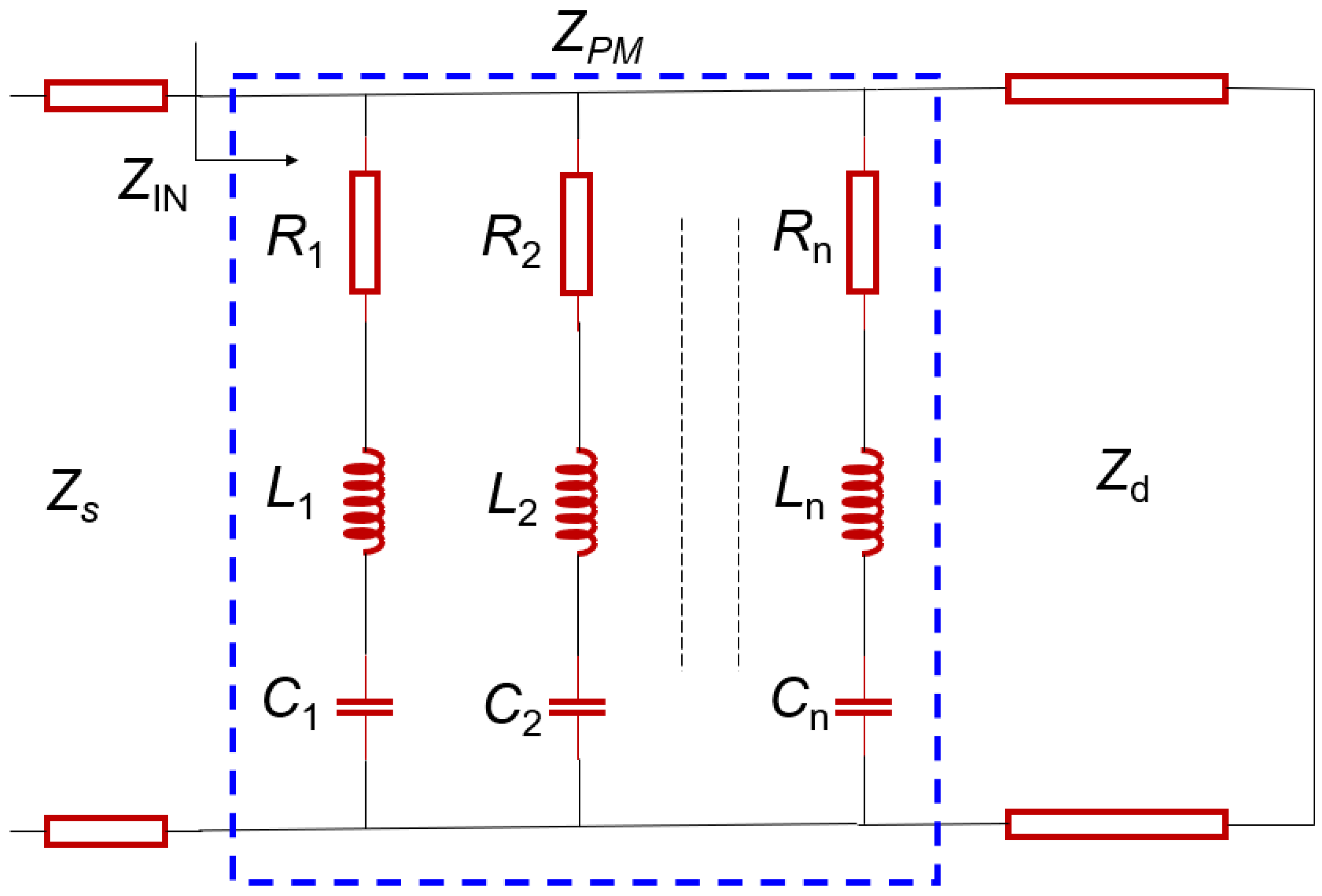
The plasmonic metasurface, as illustrated in Figure 1, can be described in terms of an equivalent circuit model based on the transmission line theory [35]. The plasmonic metasurface is represented by a combination of circuit elements connected together, as shown in the circuit diagram in Figure 2. The impedance of free space is represented by Zs. Subsequently, the circular structure is modeled by the RLC circuits. The dielectric substrate is represented by impedance Zd. Finally, the continuous copper layer on the backside of the dielectric layer is considered a short-circuit component in the circuit model [36].
From the equivalent circuit, the input impedance of plasmonic metasurface can be calculated by using the following formula:
Z I N = Z P M Z d Z P M + Z d .
ZPM is the impedance of the circular structure of the plasmonic metasurface and is calculated from the parallel RLC circuit components, as shown below.
1 Z P M = 1 Z 1 + 1 Z 2 + 1 Z n
where
Z i = R i + j ω L i + 1 j ω C i
with Ri, Li, and Ci as the resistance, inductance, and capacitance of the ith branch, respectively. In addition, n is the total number of branches in the parallel circuit.
Consequently, the reflection coefficient of the plasmonic metasurface under the incidence of an EM wave can be determined with the following expression:
Γ = Z I N Z s Z I N + Z s .
According to the transmission line theory, to obtain the minimum reflection coefficient, the input impedance should match that of the free space, as mathematically expressed in Equation (4). The input impedance of the plasmonic metasurface is composed of those of the dielectric layer and the split circular structure. These split rings were positioned very close to one another, resulting in coupling effects between them. This caused the plasmonic metasurface to function similarly to a multilayer frequency-selective surface [30]. The final outcome was the existence of a broad frequency band where the plasmonic metasurface exhibited a low reflection coefficient and high absorption.
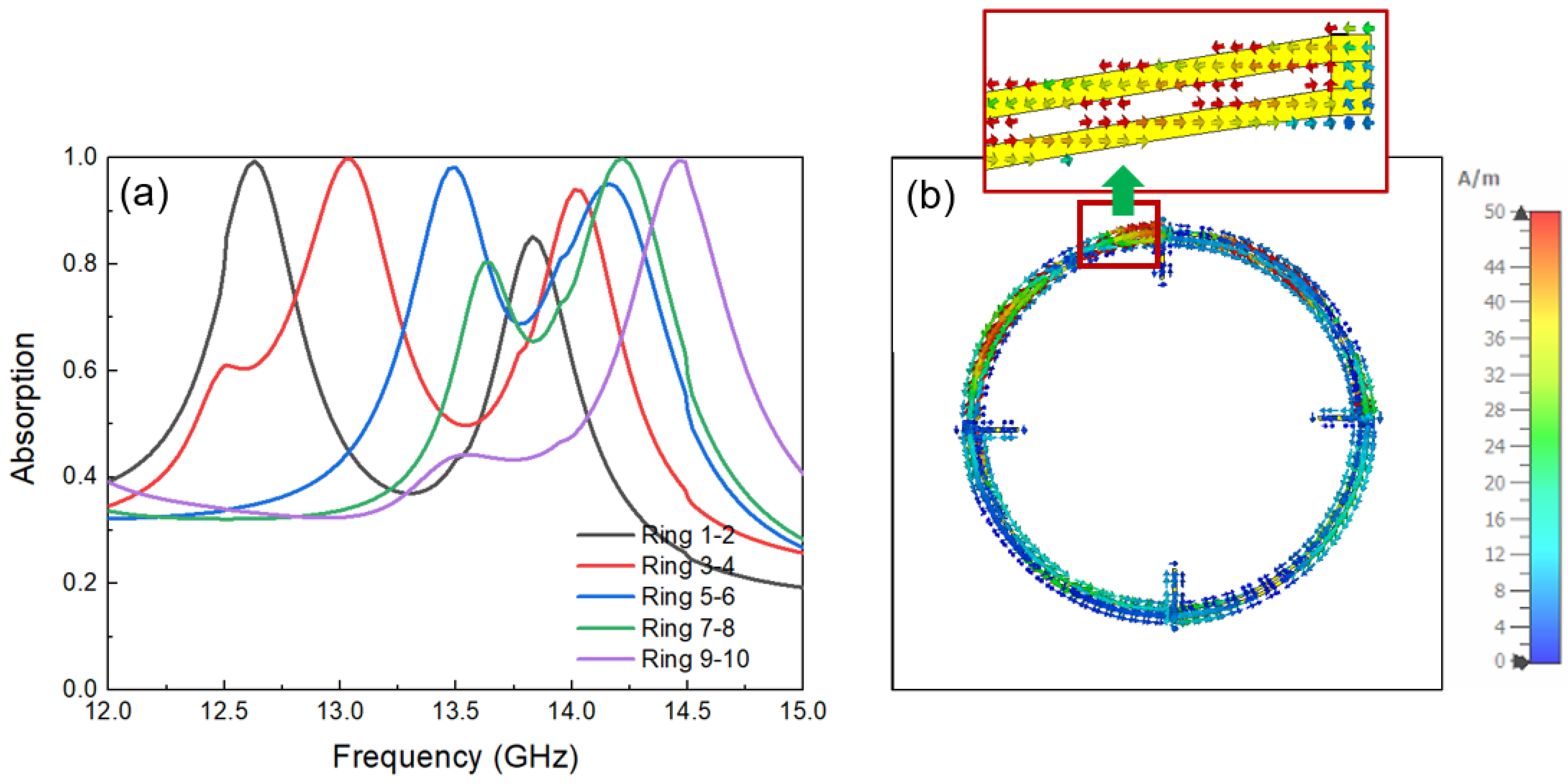
To further clarify the absorption characteristics of the plasmonic metasurface, we examined the response of the split-ring components within the structure. Figure 3a illustrates the absorption characteristics of the structure formed by pairs of adjacent split rings in the following order: Rings 1–2, 3–4, 5–6, 7–8, and 9–10, as depicted in Figure 1a. These paired split rings present the absorption spectra with two resonance peaks in a range of 12.30 to 14.80 GHz. At both end frequencies, a high absorption of over 95% is shown. The results indicate that, for the rings with smaller radii, the absorption peaks shift slightly toward higher frequencies, which can be explained by the fact that the total length of the split ring is shorter when the ring radius is smaller. It is noteworthy that the split-ring pairs can be formed not only by adjacent rings but also by any arbitrary pairing of rings. Consequently, a large number of coupled ring pairs can be generated. These coupled rings are capable of strongly absorbing EM waves across different frequency ranges. As a result, the plasmonic metasurface exhibits an overlap of multiple absorption peaks from various coupled ring pairs, leading to a broadband absorption spectrum.
Figure 3b presents the surface current distribution on a coupled ring at the resonance frequency. It can be observed that strong currents flow on its surface, and notably, the current directions on the two branches of the adjacent rings are opposite. This phenomenon can be explained by the presence of a connected bar linking the two sections. To ensure a continuous current flow within the structure, the current directions on the two branches should be opposite. These results highlight the critical role of the connecting bars in this structure. Without them, the split-ring branches in the two rings would act independently, not allowing the existence of multiple interconnected resonance peaks. This interconnection is essential in forming a broadband absorption.
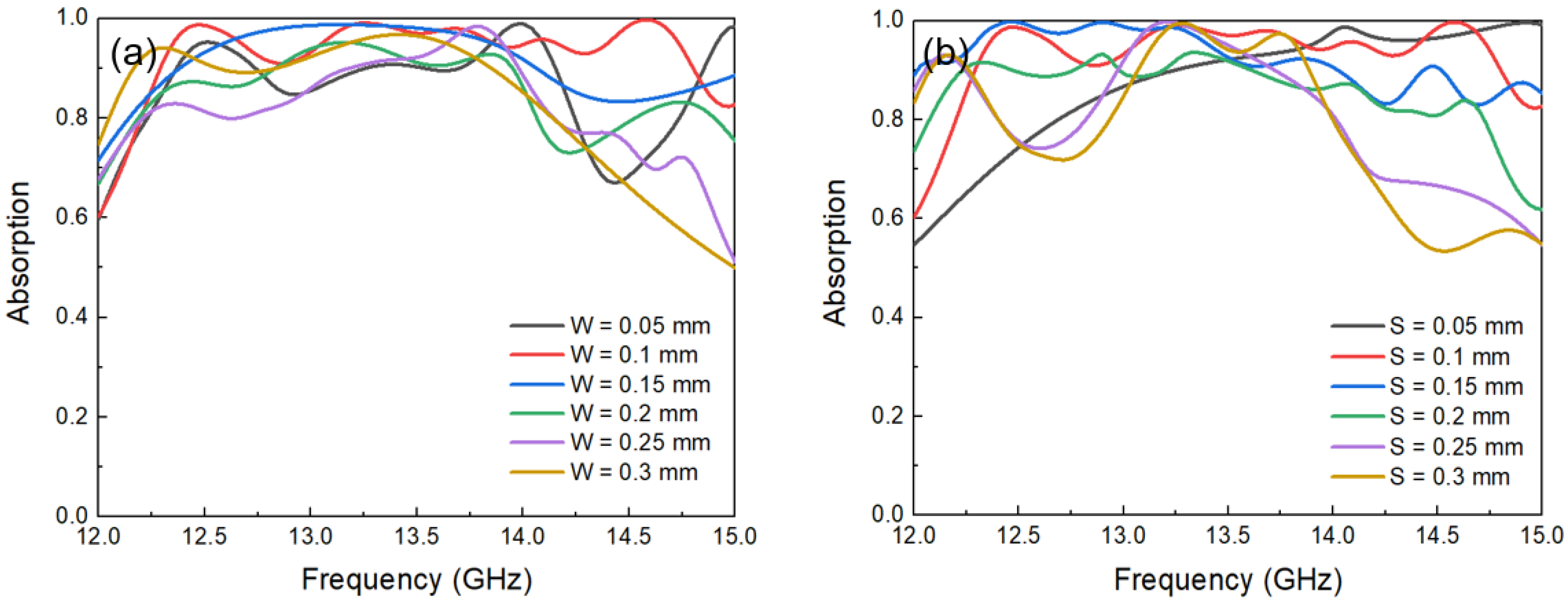
Two parameters, the strip width of ring (W) and the spacing between adjacent rings (S), are critical factors in the design of the plasmonic metasurface structure. These parameters influenced the coupling between neighboring rings as well as the overall length of split rings, thereby determining both the resonance frequency and the absorption efficiency of the structure. Therefore, we conducted an investigation on various values of W and S to identify the optimal dimensions. Figure 4a illustrates the simulated absorption performance of the plasmonic metasurface by varying the W value from 0.05 mm to 0.3 mm while keeping all the other parameters constant. The results indicate that, at W = 0.1 mm, the plasmonic metasurface shows an absorption exceeding 90% with the broadest frequency bandwidth. Similarly, Figure 4b presents the corresponding results by varying the S value from 0.05 to 0.3 mm while keeping the other parameters fixed. The results reveal that the optimal absorption performance, exceeding 90% over a wide frequency range from 12.30 GHz to 14.80 GHz, is obtained when W = 0.1 and S = 0.1 mm. Therefore, we selected W = 0.1 and S = 0.1 mm as the optimal dimensions for further studies. When observing the results in Figure 4a,b, it can be seen that, as the values of S and W increase, the broadband absorption region of the plasmonic metasurface becomes narrower. This phenomenon can be explained by the fact that the broadband absorption region of the plasmonic metasurface is formed, based on the overlap of the resonance regions of the split rings. When the spacing between the split rings increases, this overlap is reduced, thereby narrowing the broadband absorption frequency range as well as the absorption itself.
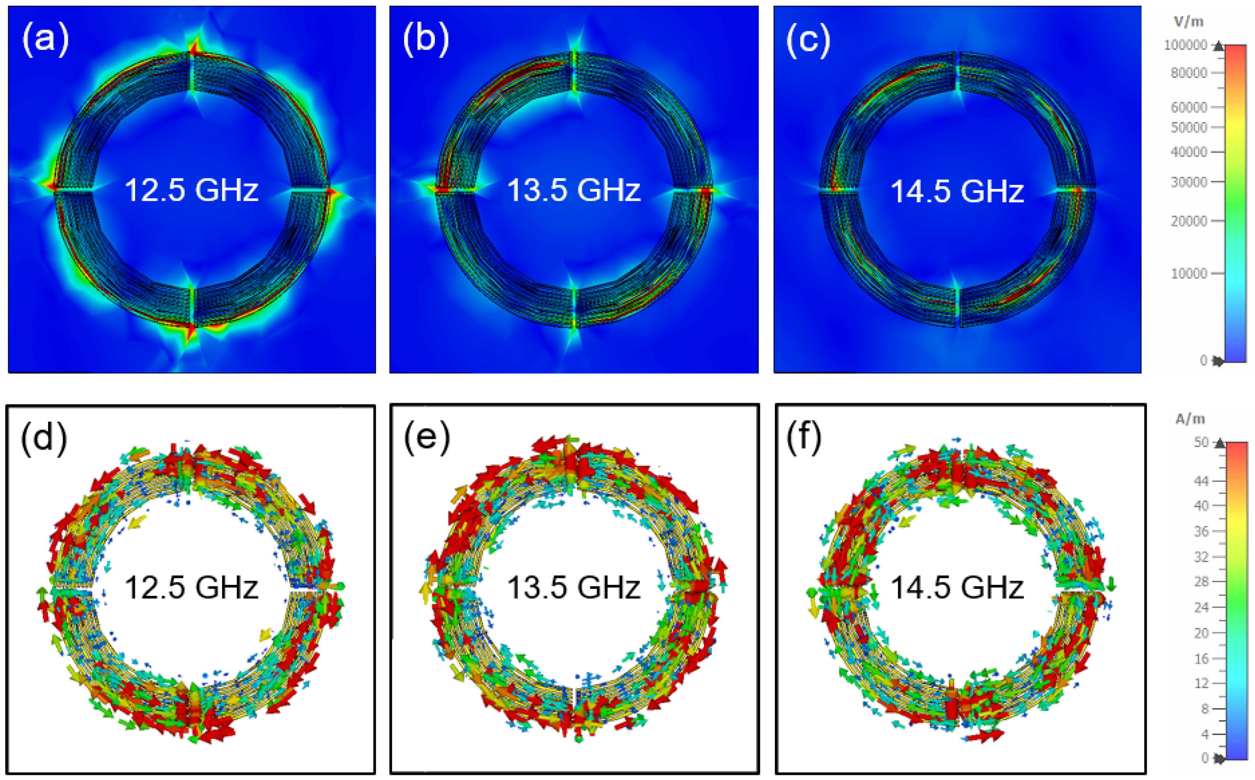
To better understand the underlying mechanisms responsible for the broadband absorption of the plasmonic metasurface, it is critical to examine the distributions of the E-field and surface current within the structure. Figure 5a–c provide a detailed visualization of the E-field distributions across the plasmonic metasurface at three representative frequencies: 12.5, 13.5, and 14.5 GHz. The components of this field represent the absolute value of the E-field on plane z = 0. The directions of the field are not considered here. Instead, we focus on observing the direction of the surface current flow within the structure later. It should be noted that, at all three frequencies, the metasurface showed an absorption exceeding 90%, as in Figure 4, highlighting its efficiency in capturing EM energy. However, the spatial distribution of the E-field reveals significant variation depending on the frequency, indicating that different regions of the metasurface contribute dominantly to the absorption at different frequencies.
At a frequency of 12.5 GHz, which corresponds to a wavelength of approximately 24 mm, the strongest E-field concentration is observed at the outermost cut circular segments of the plasmonic metasurface structure. These regions, located at the periphery of design, act as hotspots for field enhancement and play a critical role in the absorption process at lower frequencies. As the frequency increases to 13.5 GHz (wavelength ~ 22.2 mm) and further to 14.5 GHz (wavelength ~ 20.6 mm), the regions of maximum E-field intensity progressively shift inward, focusing on the smaller-diameter split rings closer to the center of the structure. This inward movement of the E-field intensity with an increasing frequency suggests a frequency-selective interaction between the EM wave and structural elements of the plasmonic metasurface, highlighting the role of geometric scaling in determining the resonant behavior of different regions. The results of the field distribution, which depend on the positions of the split rings within the unit cell, can be explained by the fact that each split ring with a different length resonates at a different frequency of the incident EM wave. The relationship between the length of the split ring and its resonance frequency can be expressed by the following formula [37]:
f ij = c i 2 + j 2 2 L ɛ eff
where i and j are integers (0, 1, 2…), i2 + j2 ≠ 0, and ɛeff is the effective dielectric constant.
Based on Equation (5), the operating frequency of the structure is inversely proportional to the length of the split ring. Therefore, the split rings located on the inner side respond to higher frequencies of the EM waves, and vice versa.
In addition to the E-field distributions, Figure 5e,f present the surface current distributions within the plasmonic metasurface at the same frequencies. These current distributions provide further insights into the physical mechanism that governs the broadband absorption. The regions exhibiting strong E-field intensities in Figure 5a–c are found to correspond to the areas with significant surface currents. Notably, the current distribution reveals that adjacent split rings form continuous current paths, resulting in a unique current flow pattern. Specifically, the currents in neighboring loops flow in opposite directions, developing localized magnetic dipoles that contribute to the absorption properties of the plasmonic metasurface. These opposite current directions are a direct consequence of the structural design with connecting bars.
A key feature of the metasurface design is the presence of connecting bars at the ends of split rings. These connecting bars play a crucial role in enabling current flow between adjacent rings. This connectivity facilitates the coupling and overlapping of resonances between different structural elements, thereby enhancing the capability of the metasurface to absorb EM waves across a wide frequency range. The coupling effect, combined with the structural geometry of the split rings, leads to the formation of multiple absorption peaks that overlap, resulting in the observed broadband absorption.

3. Experimental Verification for the Proposed Plasmonic Metasurface

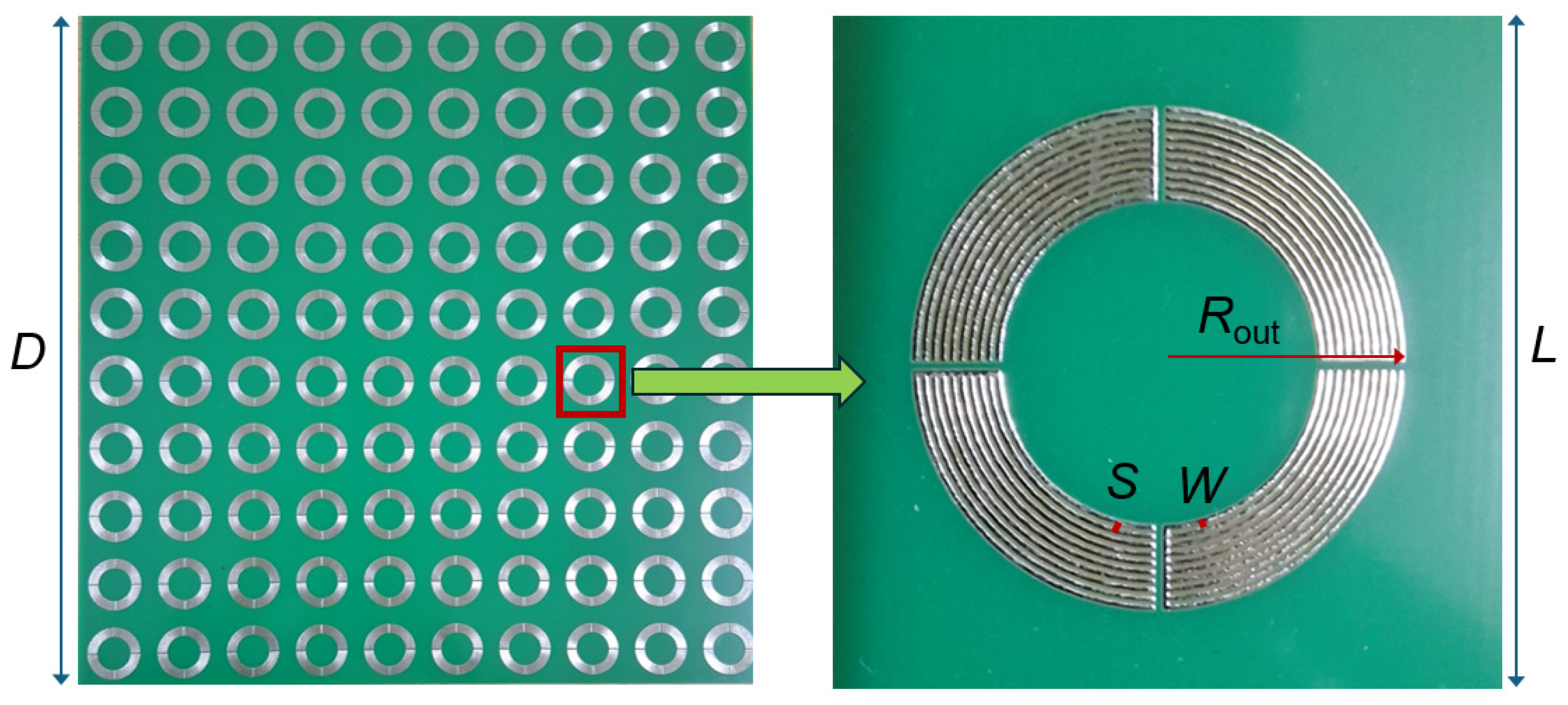
The proposed plasmonic metasurface, which was analyzed above, was fabricated as shown in Figure 6. The metasurface consisted of a 10 × 10 array of unit cells, as described here and in Figure 1, with the following parameters: D = 187 mm, L = 18.7 mm, Rout = 7 mm, W = 0.1 mm, and S = 0.1 mm. The plasmonic metasurface was fabricated by using the standard PCB technology on an FR-4 substrate with a thickness of 3.2 mm. The copper layers on both the top and bottom surfaces of the structure had a thickness of 0.035 mm and conductivity of 5.96 × 10⁷ S/m. FR-4 is a highly durable material resistant to environmental factors such as mechanical, temperature, and chemical factors, while the copper layer, manufactured by using the standard PCB technology, exhibits excellent adhesion to the FR-4 substrate. This method is widely employed in the fabrication of electronic circuits and antennas owing to its high durability [38]. The structure comprised only three layers, and with the dimensions of the unit cell as specified above, it was relatively straightforward to fabricate. This simplicity is one of the advantages of the proposed plasmonic metasurface by utilizing the SSPP effect, compared to multilayered or 3D structures commonly employed in MPA designs. The overall size of the fabricated plasmonic metasurface was 187 × 187 mm. The detailed geometrical parameters of the proposed plasmonic metasurface are presented in Table 1.
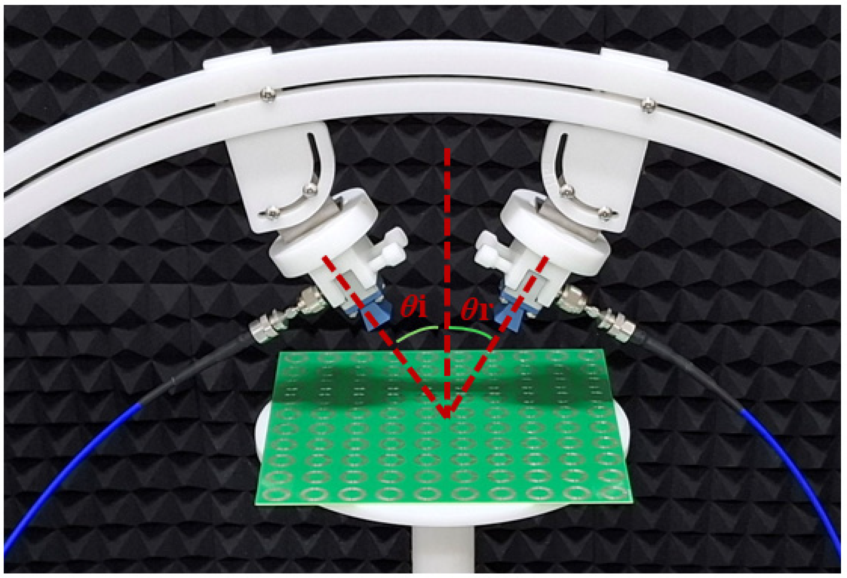
The plasmonic metasurface was characterized by using a Rohde & Schwarz ZNB20 Vector Network Analyzer (VNA) and a pair of wideband antennas operating in a frequency range of 12 to 18 GHz, as shown in Figure 7. The two antennas were connected to the two ports of the VNA, enabling the transmission of EM waves toward the structure and the reception of reflected waves. After the calibration process of the VNA, the reflection coefficient (S11) of the plasmonic metasurface was determined through the transmission coefficient (S21) from the transmitting antenna to the receiving one. Since the back side of the structure consisted of a continuous copper layer, EM waves could not transmit through the structure, and the absorption of the plasmonic metasurface was calculated by employing formula A = 1 − |S11|2. To measure the incident angle dependence of the plasmonic metasurface, the two antennas were rotated and moved along an arc-shaped support, ensuring that the incident angle θi equals the reflection angle θr.
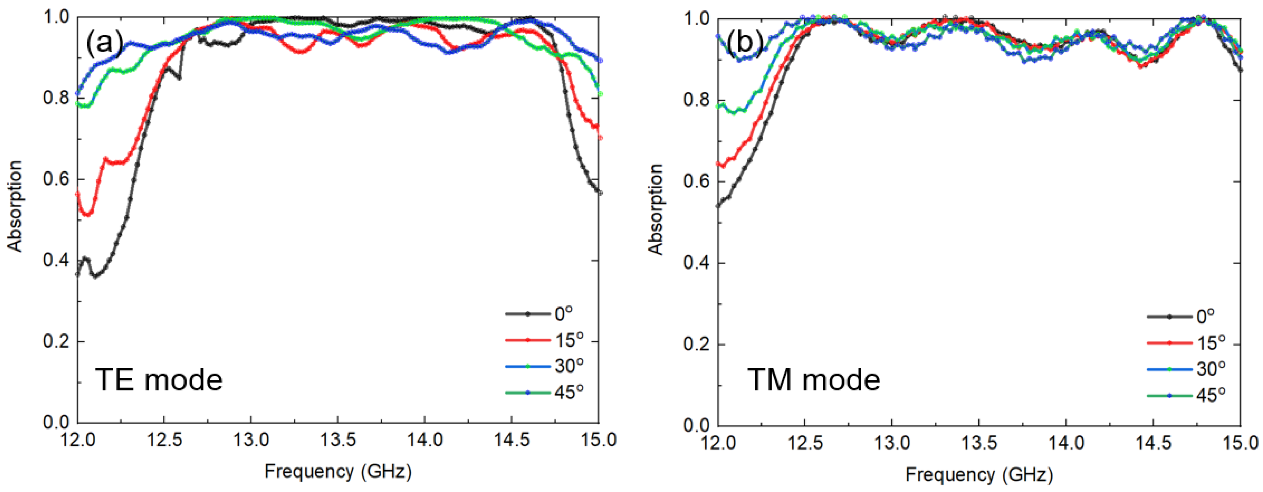
Figure 8a presents the measured absorption performance of the plasmonic metasurface for the TE-polarized waves at incidence angles ranging from 0 to 45°. The results demonstrate that the plasmonic metasurface realized an absorption over 90% of the incident wave within a frequency range of 12.40 to 14.75 GHz. At larger incidence angles, the absorption bandwidth becomes broader (e.g., 12.10 to 14.90 GHz at 45°) compared to smaller incidence angles. This could be attributed to the parallel component of the EM waves interacting with the plasmonic metasurface in a manner similar to 3D structures, where metal bars aligned with the direction of the incident EM wave contributed to the absorption. When compared to the absorption spectrum obtained from simulations, the measured values exhibit some discrepancies. However, the broadband absorption characteristic and high absorption exceeding 90% of the plasmonic metasurface are still preserved. The observed differences might stem from the fabrication process of the plasmonic metasurface, since small fabrication errors can influence the interactions between the split rings in the unit cell structure. Nevertheless, these interactions might compensate for each other, ensuring that the quality of the absorption spectrum of the plasmonic metasurface is not significantly affected. Moreover, the discrepancies might also derive from the measurement process, since we used a VNA to measure the reflection coefficient (S11) of the plasmonic metasurface, from which the absorption performance was calculated. The antennas might have been placed at slightly misaligned positions, and certain unavoidable unwanted interactions could also contribute to these differences.
Figure 8b illustrates the absorption performance of the plasmonic metasurface for TM-polarized waves. Due to the design of the circular unit cell of the structure, the symmetry is relatively high, resulting in an absorption spectrum for the TM waves, which is quite similar to that of the TE mode. The metasurface provided an absorption over 90% in a frequency range of 12.40 to 14.90 GHz for the TM-polarized waves. Naturally, slight differences between the TE and TM modes remained, attributed to the inherent properties of the metasurface and the measurement inaccuracies discussed above.
For both TE and TM modes, the absorption spectrum is not completely flat at a level of 90% across the frequency range. Instead, it reaches 99% at certain frequencies for all incident angles. This behavior can be explained by the unequal interaction of the split-ring pairs forming the metasurface. Nevertheless, the lowest absorption level remains above 90%, making the metasurface suitable for applications requiring a high absorption efficiency.

4. Discussion

Metamaterials with ring and split-ring structures have been extensively studied for broadband absorption applications, yielding significant results [39,40,41,42,43,44]. However, the achievement of broadband absorption in previous studies often required the use of external electrical components, multilayer structures, or specialized materials. For instance, in Ref. [39], Li et al. obtained an absorption exceeding 90% at incident angles from 0 to 30° within a frequency range of 7.93 to 17.18 GHz using a double octagonal ring structure. However, this design necessitated the integration of four resistors into each unit cell, where the resistors functioned as energy absorption points, contributing to the broadband absorption performance of the structure. Similarly, in Ref. [40], the proposed absorber prototype demonstrated an absorption exceeding 80% across a frequency range of 5.46 to 14.75 GHz, with an incident angle tolerance up to 30°. To achieve this result, the metamaterial absorber was fabricated as a multilayer structure, incorporating two layers of double split-serration rings (DSSRs) sandwiched between three layers of modified epoxy with varying thicknesses. Additionally, several other structures have been proposed for broadband absorption. However, these designs typically required the use of four resistors per unit cell [41,42] or even eight ones per unit cell [43]. In cases where resistors are not employed, the proposed structures tended to rely on multilayer configurations and specialized materials, such as indium tin oxide combined with air gaps [44].
In other studies [45,46] that did not employ external electrical components or specialized materials, achieving broadband absorption still remained challenging. Instead, these studies often resulted in multi-peak absorption [45]. Occasionally, broadband absorption was achieved; however, the absorption bandwidth was typically less than 1 GHz [46]. In contrast, our proposed plasmonic design features a simple configuration based on a metal-–dielectric–metal structure. The top copper layer was fabricated by using the standard PCB technology, which was highly straightforward and ensured high reproducibility. No resistors or external components are required in this plasmonic metasurface. Consequently, our proposed design achieved a broadband absorption within a range of 12.30 to 14.80 GHz. When compared to the previous results that used lumped elements/multilayer, our reported relative absorption bandwidth of 18.45% is indeed narrow. However, when compared to the publications without the use of lumped elements/multilayer, the 18.45% bandwidth is significantly larger, since the previous publications have reported values of 1.18%, 2.46%, and 6.46%, respectively (see Table 2). This approach offers significant advantages in terms of compactness, ease of fabrication, and cost-effectiveness. A detailed comparison of the performance of this work with previous studies is presented in Table 2.

5. Conclusions

This study proposes a plasmonic metasurface structure capable of absorbing over 90% of EM waves in a broad frequency range from 12.30 to 14.80 GHz. Simulation and experimental studies demonstrated that the plasmonic metasurface maintained a high absorption and wide bandwidth for both TE and TM waves, for incident angles up to 45°. Notably, the broadband absorption was obtained without the use of external elements such as resistors or specialized materials. The structure was 2D and was easily fabricated using the standard PCB technology. Due to its simple and compact design, the plasmonic metasurface also exhibited high durability and was more practical for implementation compared to previously proposed structures that relied on complex fabrication techniques. Given its advantages, the plasmonic metasurface has potential for various applications, including radar stealth technology, satellite communications, surveillance radars, and many other promising fields.

Author Contributions

Conceptualization, T.S.P. and B.X.K.; methodology, T.S.P.; software, B.X.K.; validation, V.D.L. and Y.L.; formal analysis, T.S.P.; investigation, B.X.K.; resources, V.D.L.; data curation, B.X.K.; writing—original draft preparation, T.S.P.; writing—review and editing, Y.L., V.D.L., and L.C.; supervision, Y.L.; project administration, Y.L. and V.D.L. All authors have read and agreed to the published version of the manuscript.

Funding

This research was funded by the Vietnam Academy of Science and Technology, under grant number NCPTVL.03/24/25, supported by the Shanghai Science and Technology Commission, under grant number 24110714600, and funded by the Korea Evaluation Institute of Industrial Technology (Project No. 20016179).

Institutional Review Board Statement

Not applicable.

Informed Consent Statement

Not applicable.

Data Availability Statement

The data used and/or analyzed during the current study are available from the corresponding author upon reasonable request.

Conflicts of Interest

The authors declare no conflicts of interest.

References

  1. Xiao, S.; Wang, T.; Liu, T.; Zhou, C.; Jiang, X.; Zhang, J. Active Metamaterials and Metadevices: A Review. J. Phys. D Appl. Phys. 2020, 53, 503002. [Google Scholar] [CrossRef]
  2. Kadic, M.; Milton, G.W.; van Hecke, M.; Wegener, M. 3D Metamaterials. Nat. Rev. Phys. 2019, 1, 198–210. [Google Scholar] [CrossRef]
  3. Nguyen, H.A.; Pham, T.S.; Tung, B.S.; Khuyen, B.X.; Le, D.T.; Vu, H.Y.; Vu, D.L.; Hien, N.T. Metamaterials Based on Hyperbolic-Graphene Composite: A Pathway from Positive to Negative Refractive Index at Terahertz. Comput. Mater. Sci. 2025, 248, 113574. [Google Scholar] [CrossRef]
  4. Fowler, C.; Silva, S.; Thapa, G.; Zhou, J. High Efficiency Ambient RF Energy Harvesting by a Metamaterial Perfect Absorber. Opt. Mater. Express OME 2022, 12, 1242–1250. [Google Scholar] [CrossRef]
  5. Hiep, L.T.H.; Bui, H.N.; Tung, B.S.; Lam, V.D.; Khuyen, B.X.; Pham, T.S. Enhanced Efficiency of Magnetic Resonant Wireless Power Transfer System Using Rollable and Foldable Metasurface Based on Polyimide Substrate. Appl. Phys. A 2024, 130, 521. [Google Scholar] [CrossRef]
  6. Rakhshani, M.R.; Rashki, M. Metamaterial Perfect Absorber Using Elliptical Nanoparticles in a Multilayer Metasurface Structure with Polarization Independence. Opt. Express OE 2022, 30, 10387–10399. [Google Scholar] [CrossRef]
  7. Bhati, R.; Malik, A.K. Multiband Terahertz Metamaterial Perfect Absorber for Microorganisms Detection. Sci. Rep. 2023, 13, 19685. [Google Scholar] [CrossRef]
  8. Tung, B.S.; Viet, N.N.; Khuyen, B.X.; Pham, T.S.; Do, P.X.; Hoa, N.T.; Lam, V.D.; Tung, D.K. Multi-Band and Polarization-Insensitive Electromagnetically-Induced Transparency Based on Coupled-Resonators in a Metamaterial Operating at GHz Frequencies. Phys. Scr. 2024, 99, 115502. [Google Scholar] [CrossRef]
  9. Shruti; Pahadsingh, S.; Appasani, B. Metamaterial-Based Terahertz Absorbers for Refractive Index Sensing: Types, Mechanism, and Applications. Plasmonics 2024. [Google Scholar] [CrossRef]
  10. Saadeldin, A.S.; Sayed, A.M.; Amr, A.M.; Sayed, M.O.; Hameed, M.F.O.; Obayya, S.S.A. Wideband Ultrathin and Polarization Insensitive Metamaterial Absorber for Ku-Band Applications. J. Mater. Sci. Mater. Electron. 2023, 34, 1797. [Google Scholar] [CrossRef]
  11. Tan, T.; Yan, Z.; Zou, H.; Ma, K.; Liu, F.; Zhao, L.; Peng, Z.; Zhang, W. Renewable Energy Harvesting and Absorbing via Multi-Scale Metamaterial Systems for Internet of Things. Appl. Energy 2019, 254, 113717. [Google Scholar] [CrossRef]
  12. Wang, C. Design, Calculation, and Measurement of a Single Resonant Mode Metamaterial Absorber and Its Tunable Performance. Opt. Mater. 2024, 148, 114810. [Google Scholar] [CrossRef]
  13. Liu, Y.; Ma, W.-Z.; Wu, Y.-C.; Meng, D.; Cheng, Y.-Y.; Chen, Y.-S.; Liu, J.; Gu, Y. Multi-Peak Narrow-Band Metamaterial Absorber for Visible to near-Infrared Wavelengths. Results Phys. 2023, 47, 106374. [Google Scholar] [CrossRef]
  14. Zheng, H.; Pham, T.S.; Chen, L.; Lee, Y. Metamaterial Perfect Absorbers for Controlling Bandwidth: Single-Peak/Multiple-Peaks/Tailored-Band/Broadband. Crystals 2024, 14, 19. [Google Scholar] [CrossRef]
  15. Ullah, N.; Islam, M.S.; Hoque, A.; Yong, W.H.; Alrashdi, A.M.; Soliman, M.S.; Islam, M.T. An Efficient, Compact, Wide-Angle, Wide-Band, and Polarization-Insensitive Metamaterial Electromagnetic Energy Harvester. Alex. Eng. J. 2023, 82, 377–388. [Google Scholar] [CrossRef]
  16. Zhang, C.; Yin, S.; Long, C.; Dong, B.W.; He, D.; Cheng, Q. Hybrid Metamaterial Absorber for Ultra-Low and Dual-Broadband Absorption. Opt. Express OE 2021, 29, 14078–14086. [Google Scholar] [CrossRef]
  17. Liang, C.; Kong, X.; Wang, F.; Xu, R.; Fu, Y.; Pang, X.; Zhang, S.; Shen, X.; Zhao, L. A Broadband Perfect Metamaterial Absorber with Angle-Insensitive Characteristics. J. Electromagn. Waves Appl. 2023, 37, 401–410. [Google Scholar] [CrossRef]
  18. Feng, S.; Yang, L.; Cai, B.; Yang, W.; Wu, L.; Cheng, Y.; Chen, F.; Luo, H.; Li, X. Tri-Band Terahertz Metamaterial Absorber Based on Structural Ti3C2Tx MXene for Enhanced Sensing Application. IEEE Sens. J. 2024, 24, 28889–28896. [Google Scholar] [CrossRef]
  19. You, X.; Upadhyay, A.; Cheng, Y.; Bhaskaran, M.; Sriram, S.; Fumeaux, C.; Withayachumnankul, W. Ultra-Wideband Far-Infrared Absorber Based on Anisotropically Etched Doped Silicon. Opt. Lett. OL 2020, 45, 1196–1199. [Google Scholar] [CrossRef]
  20. Shen, Z.; Huang, D.; Lin, X. Dual-Band Chirality-Selective Absorbing by Plasmonic Metasurfaces with Breaking Mirror and Rotational Symmetry. Opt. Express OE 2023, 31, 35730–35741. [Google Scholar] [CrossRef]
  21. Pendry, J.B.; Martín-Moreno, L.; Garcia-Vidal, F.J. Mimicking Surface Plasmons with Structured Surfaces. Science 2004, 305, 847–848. [Google Scholar] [CrossRef] [PubMed]
  22. Pham, T.S.; Zheng, H.; Chen, L.; Khuyen, B.X.; Lee, Y. Wide-Incident-Angle, Polarization-Independent Broadband-Absorption Metastructure without External Resistive Elements by Using a Trapezoidal Structure. Sci. Rep. 2024, 14, 10198. [Google Scholar] [CrossRef] [PubMed]
  23. Zhu, R.; Wang, J.; Sui, S.; Meng, Y.; Qiu, T.; Jia, Y.; Wang, X.; Han, Y.; Feng, M.; Zheng, L.; et al. Wideband Absorbing Plasmonic Structures via Profile Optimization Based on Genetic Algorithm. Front. Phys. 2020, 8, 231. [Google Scholar] [CrossRef]
  24. Garcia-Vidal, F.J.; Fernández-Domínguez, A.I.; Martin-Moreno, L.; Zhang, H.C.; Tang, W.; Peng, R.; Cui, T.J. Spoof Surface Plasmon Photonics. Rev. Mod. Phys. 2022, 94, 025004. [Google Scholar] [CrossRef]
  25. Tang, W.X.; Zhang, H.C.; Ma, H.F.; Jiang, W.X.; Cui, T.J. Concept, Theory, Design, and Applications of Spoof Surface Plasmon Polaritons at Microwave Frequencies. Adv. Opt. Mater. 2019, 7, 1800421. [Google Scholar] [CrossRef]
  26. Cheng, Z.W.; Wang, M.; You, Z.H.; Ma, H.F.; Cui, T.J. Spoof Surface Plasmonics: Principle, Design, and Applications. J. Phys. Condens. Matter 2022, 34, 263002. [Google Scholar] [CrossRef]
  27. Gu, Z.; Ma, Q.; Gao, X.; You, J.W.; Cui, T.J. Direct Electromagnetic Information Processing with Planar Diffractive Neural Network. Sci. Adv. 2024, 10, eado3937. [Google Scholar] [CrossRef]
  28. Gao, X.; Gu, Z.; Ma, Q.; Chen, B.J.; Shum, K.-M.; Cui, W.Y.; You, J.W.; Cui, T.J.; Chan, C.H. Terahertz Spoof Plasmonic Neural Network for Diffractive Information Recognition and Processing. Nat. Commun. 2024, 15, 6686. [Google Scholar] [CrossRef]
  29. Jidi, L.; Cao, X.; Gao, J.; Li, T.; Yang, H.; Li, S. Ultra-Wideband Absorber for Electromagnetic Waves under Large Incident Angle Based on Spoof Surface Plasmon Polaritons. Opt. Mater. Express OME 2021, 11, 3917–3929. [Google Scholar] [CrossRef]
  30. Bai, J.; Yang, Q.; Liang, Y.; Gao, X. Broadband Frequency Selective Rasorber Based on Spoof Surface Plasmon Polaritons. Micromachines 2022, 13, 1969. [Google Scholar] [CrossRef]
  31. Jiang, W.; Ma, H.; Wang, J.; Yang, J.; Yan, L.; Fan, Y.; Qu, S. Spoof Surface Plasmon Polaritons Realized by Unidirectional Carbon Fibers Arrays and Applications in Structure/Function Integrated Sandwich Structure. Results Phys. 2020, 17, 103081. [Google Scholar] [CrossRef]
  32. Zhou, S.; Liang, X.; Xing, J.; Fan, Y.; Zhang, L.; Li, D.; Li, E.-P. Ultra-Broadband Metamaterial Absorbers Based on Spoof Surface Plasmon Polaritons Structure. Microw. Opt. Technol. Lett. 2022, 64, 489–495. [Google Scholar] [CrossRef]
  33. Xu, J.; Zhao, Z.; Yu, H.; Yang, L.; Gou, P.; Cao, J.; Zou, Y.; Qian, J.; Shi, T.; Ren, Q.; et al. Design of Triple-Band Metamaterial Absorbers with Refractive Index Sensitivity at Infrared Frequencies. Opt. Express OE 2016, 24, 25742–25751. [Google Scholar] [CrossRef]
  34. CST Studio Suite 3D EM Simulation and Analysis Software. Available online: https://www.3ds.com/products-services/simulia/products/cst-studio-suite/ (accessed on 10 October 2023).
  35. Chen, H.; Yang, X.; Wu, S.; Zhang, D.; Xiao, H.; Huang, K.; Zhu, Z.; Yuan, J. Flexible and Conformable Broadband Metamaterial Absorber with Wide-Angle and Polarization Stability for Radar Application. Mater. Res. Express 2018, 5, 015804. [Google Scholar] [CrossRef]
  36. Jeong, H.; Lim, S. Broadband Frequency-Reconfigurable Metamaterial Absorber Using Switchable Ground Plane. Sci. Rep. 2018, 8, 9226. [Google Scholar] [CrossRef]
  37. Yoo, Y.J.; Kim, Y.J.; Hwang, J.S.; Rhee, J.Y.; Kim, K.W.; Kim, Y.H.; Cheong, H.; Chen, L.Y.; Lee, Y.P. Triple-Band Perfect Metamaterial Absorption, Based on Single Cut-Wire Bar. Appl. Phys. Lett. 2015, 106, 071105. [Google Scholar] [CrossRef]
  38. Sandeep, D.R.; Sivanvitha, G.V. Design of Low-Cost Compact FR-4 Microstrip Patch Antenna for 5G, ISM, and X-Band Applications. In Proceedings of the 2024 IEEE Wireless Antenna and Microwave Symposium (WAMS), Visakhapatnam, India, 29 February–3 March 2024; pp. 1–5. [Google Scholar]
  39. Li, S.; Gao, J.; Cao, X.; Li, W.; Zhang, Z.; Zhang, D. Wideband, Thin, and Polarization-Insensitive Perfect Absorber Based the Double Octagonal Rings Metamaterials and Lumped Resistances. J. Appl. Phys. 2014, 116, 043710. [Google Scholar] [CrossRef]
  40. Li, S.-J.; Cao, X.-Y.; Gao, J.; Liu, T.; Zheng, Y.-J.; Zhang, Z. Analysis and Design of Three-Layer Perfect Metamaterial-Inspired Absorber Based on Double Split-Serration-Rings Structure. IEEE Trans. Antennas Propag. 2015, 63, 5155–5160. [Google Scholar] [CrossRef]
  41. Nguyen, T.Q.H.; Nguyen, T.K.T.; Cao, T.N.; Nguyen, H.; Bach, L.G. Numerical Study of a Broadband Metamaterial Absorber Using a Single Split Circle Ring and Lumped Resistors for X-Band Applications. AIP Adv. 2020, 10, 035326. [Google Scholar] [CrossRef]
  42. Shukoor, M.A.; Dey, S. A Novel Modified Circular Ring-Based Broadband Polarization-Insensitive Angular Stable Circuit Analog Absorber (CAA) for RCS Applications. Int. J. Microw. Wirel. Technol. 2023, 15, 440–453. [Google Scholar] [CrossRef]
  43. Sambhav, S.; Ghosh, J.; Singh, A.K. Ultra-Wideband Polarization Insensitive Thin Absorber Based on Resistive Concentric Circular Rings. IEEE Trans. Electromagn. Compat. 2021, 63, 1333–1340. [Google Scholar] [CrossRef]
  44. Zheng, Y.; Chen, K.; Jiang, T.; Zhao, J.; Feng, Y. Multi-Octave Microwave Absorption via Conformal Metamaterial Absorber with Optical Transparency. J. Phys. D Appl. Phys. 2019, 52, 335101. [Google Scholar] [CrossRef]
  45. Hakim, M.L.; Alam, T.; Soliman, M.S.; Sahar, N.M.; Baharuddin, M.H.; Almalki, S.H.A.; Islam, M.T. Polarization Insensitive Symmetrical Structured Double Negative (DNG) Metamaterial Absorber for Ku-Band Sensing Applications. Sci. Rep. 2022, 12, 479. [Google Scholar] [CrossRef]
  46. Hannan, S.; Islam, M.T.; Almutairi, A.F.; Faruque, M.R.I. Wide Bandwidth Angle- and Polarization-Insensitive Symmetric Metamaterial Absorber for X and Ku Band Applications. Sci. Rep. 2020, 10, 10338. [Google Scholar] [CrossRef]
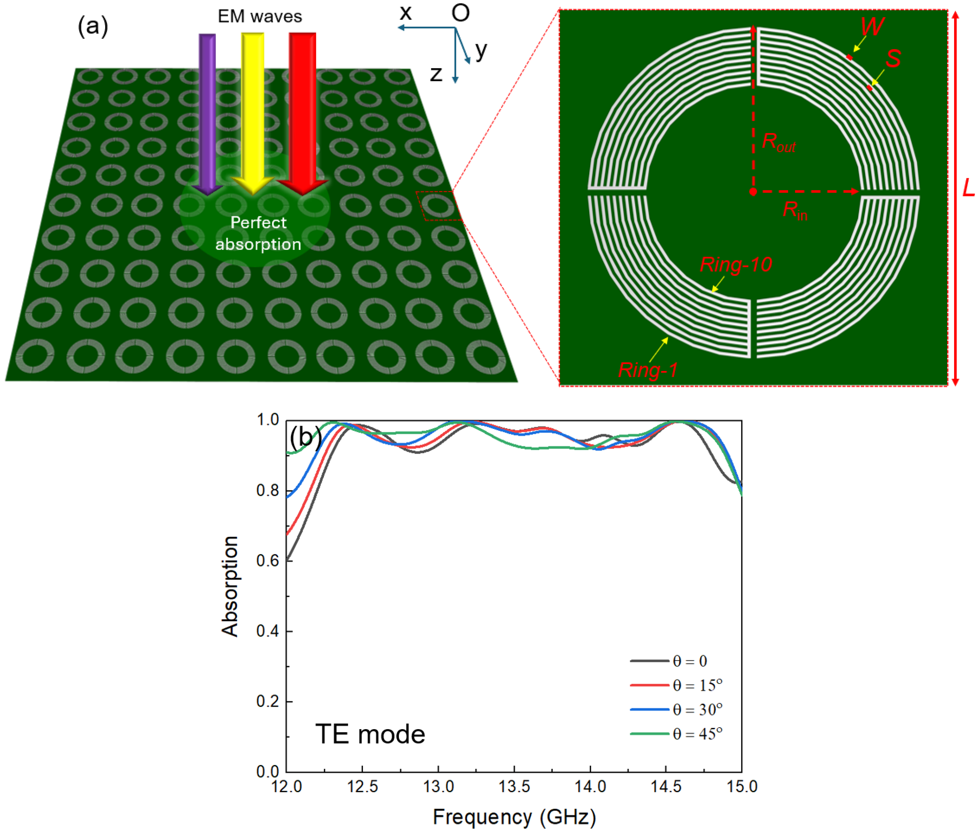
Figure 1. (a) Schematic illustration of the plasmonic metasurface and its unit cell, and (b) high absorption at various incident angles.
Photonics 12 00334 g001
Figure 2. Equivalent circuit model for the plasmonic metasurface.
Photonics 12 00334 g002
Figure 3. (a) Comparison of the absorption of coupled rings, and (b) surface current distribution on the adjacent coupled ring.
Photonics 12 00334 g003
Figure 4. Comparison of the absorption of plasmonic metasurfaces with structural parameters L = 18.7, Rout = 7, and FR-4 thickness tsub = 3.2 mm. (a) S = 0.1 and W = 0.05–0.3 mm. (b) W = 0.1 and S = 0.05–0.3 mm.
Photonics 12 00334 g004
Figure 5. (ac) E-field intensity distributions in the plasmonic metasurface at various frequencies. (df) Analysis on the surface current distribution of the plasmonic metasurface at the specific frequencies corresponding to the investigated E-field distributions.
Photonics 12 00334 g005
Figure 6. Fabricated plasmonic metasurface and its unit cell.
Photonics 12 00334 g006
Figure 7. Experiment setup for measuring the absorption of the proposed plasmonic metasurface.
Photonics 12 00334 g007
Figure 8. Measured absorption of the plasmonic metasurface at various incident angles for the (a) TE and (b) TM modes.
Photonics 12 00334 g008
Table 1. Geometrical parameters of the plasmonic metasurface.
Structure ParametersValue
Unit-cell periodicity (L)18.7 mm
Dielectric thickness (td)3.2 mm
Dielectric constant (ε)4.3
Loss tangent (tan δ)0.025
Metal thickness (tm)0.035 mm
Width of metal trace (W)0.1 mm
Spacing between turns (S)0.1 mm
Outer radius (Rout)7 mm
Number of rings (n)10
Total size of plasmonic metasurface187 × 187 mm
Table 2. Comparison of the absorption performance with other works.
Ref.Bandwidth (GHz)Relative Absorption
Bandwidth
AbsorptionLumped Elements/MultilayerPolarization
(Both TE and TM?)
Incident Angle
[39]7.93–17.1873.67%>90%Yes/NoBoth0–20°
[40]5.46–14.7591.93%>90%No/YesBoth0–30°
[41]6.80–11.8053.76%>70%Yes/NoBoth0–30°
[43]6.70–20.58101.75%>90%Yes/YesBoth0–30°
[44]6.21–19.31102.66%>90%No/YesBoth
[45]Peaks at 14.50, 16.50n/a>90%No/NoBoth0, 45°, 90°
[46]11.21–11.492.46%>90%No/NoBoth0–45°
13.92–14.856.46%
17.66–17.871.18%
This paper12.30–14.8018.45%>90%No/NoBoth0–45°
Disclaimer/Publisher’s Note: The statements, opinions and data contained in all publications are solely those of the individual author(s) and contributor(s) and not of MDPI and/or the editor(s). MDPI and/or the editor(s) disclaim responsibility for any injury to people or property resulting from any ideas, methods, instructions or products referred to in the content.