Article

Design of High-Efficiency Circularly Polarized Reflection Mirror Based on Chiral Dielectric Metasurface

1
Postdoctoral Innovation Practice Base, Chengdu Polytechnic, 83 Tianyi Street, Chengdu 610041, China
2
Sichuan Provincial Engineering Research Center of Thermoelectric Materials and Devices, Chengdu 610041, China
3
Kunming Institute of Physics, Kunming 650223, China
4
National Key Laboratory of Infrared Detection Technologies, Kunming Institute of Physics, Kunming 650223, China
5
Institute of Intelligent Photonics, Nankai University, Tianjin 300071, China
6
Institute of Semiconductors, Chinese Academy of Sciences, Beijing 100083, China
*
Authors to whom correspondence should be addressed.
Photonics 2025, 12(4), 341; https://doi.org/10.3390/photonics12040341
Submission received: 12 March 2025 / Revised: 31 March 2025 / Accepted: 2 April 2025 / Published: 3 April 2025

Abstract

:
Circularly polarized lasers can directly generate circularly polarized light without requiring complex external optics, enabling applications in biosensing, environmentally friendly antibacterial treatments, and cancer cell phototherapy. However, the circular dichroism (CD) of chiral metasurface mirrors—a core component of such lasers—typically remains below 3%, limiting beam quality. Using COMSOL simulations, we broke the metasurface’s structural symmetry via displacement and rotation operations, introducing chirality to the unit cell. At 980 nm, the metasurface achieved 99.85% reflectivity and 52% CD. Multipole analysis suggests this enhancement stems from electric dipole and quadrupole coupling. Our laser design could generate micro-nano-scale chiral light, advancing applications in biophotonics, biomedicine, and life sciences.

1. Introduction

Circularly polarized light (CP) [1,2], a subset of elliptically polarized light, consists of left (LCP) and right (RCP) circularly polarized components. It exhibits equal-intensity orthogonal amplitude projections and a ±90° phase difference. CP’s strong interaction with optically active materials makes it valuable in biological research [3,4]. In cell imaging, CP outperforms fluorescence imaging by providing real-time structural details through optical activity tracking [5,6] while avoiding phototoxicity and background fluorescence. For protein analysis, CP measures optical rotation to elucidate protein structure–function relationships [7,8], aiding studies of diseases like cancer and neurological disorders. CP also enables biomaterial detection by monitoring cell dynamics and investigating molecular interactions [9,10].
Circularly polarized lasers are advanced photonic devices that directly generate CP light, typically using vertical-cavity surface-emitting lasers (VCSELs) [11]. These lasers emit light perpendicular to the chip surface, providing an ideal photonic platform. Current CP laser technologies include: spin injection [12,13,14], cholesteric liquid crystal helical structures [15,16,17], and polarizer/waveplate combinations [18]. While the first two struggle with optoelectronic integration, the third suffers from size and cost limitations. Ultrathin chiral metasurfaces now promise to overcome these constraints. Metasurfaces [19,20,21,22] are artificially designed two-dimensional periodic arrays that can precisely regulate the refraction, reflection, and transmission properties of electromagnetic waves by adjusting the geometrical shapes of the structural units. The CD of metasurfaces refers to the phenomenon that there exist differences in the responses of metasurfaces to the LCP and RCP. This property originates from the chirality or asymmetric design of the metasurface structure, which is capable of selectively regulating the propagation behaviors of different circularly polarized lights. The integration of chiral metasurfaces into VCSEL cavities has become a research hotspot [23,24,25,26,27], showing improvements in pumping efficiency, temperature stability, and beam quality, offering new approaches for miniaturized, high-performance polarization devices and chiral photonics applications. However, the low CD values of current metasurfaces remain a critical bottleneck for compact CP laser development.
In this article, we first present in the Section 1 a discussion on the strong correlation between circularly polarized light and biological applications, along with current developments in circularly polarized laser technology. Subsequently, we optimize the metasurface structure to enhance both reflectivity and circular dichroism (CD). Through multipole expansion analysis and near-field electric field simulations, we elucidate the physical mechanism underlying the achieved 52% CD value. Furthermore, we evaluate potential errors in the COMSOL model and examine how dry etching process variations may affect the chiral metasurface performance. The designed circularly polarized laser shows promising potential for applications in chiral nanostructure fabrication, asymmetric catalysis, and negative refractive index material systems.

2. Materials and Methods

The circularly polarized VCSEL can directly excite chiral light sources, which can be applied in many fields such as the synthesis of chiral molecules, the dynamic control of molecular chirality, and the triggering of photochemistry. A compact chiral metasurface is typically used as the top reflector, which allows photons generated by the gain medium to be reflected back and forth in the resonant cavity between the chiral metasurface and the lower DBR, resulting in the stimulated radiation at a specific operating wavelength. There is the following relationship between the reflector and the excitation of the laser:
g t h = α i + 1 2 L l n 1 R 1 R 2
Here, g t h is the threshold gain coefficient, and when it is exceeded by the gain coefficient, the laser is able to produce a continuously stabilized laser output. L is the equivalent optical cavity length of the VCSEL. α i is the overall loss, including the mirror loss and internal loss. R 1 and R 2 correspond to the reflectivity of the top and bottom mirrors in VCSEL, respectively. It can be derived from Equation (1) that the top chiral metasurface in a circularly polarized VCSEL that can excite LCP light should have to satisfy two basic conditions. The first one is that the reflectivity of the metasurface to the LCP should be greater than 99% [11], which can make the threshold gain coefficient of the laser to be controlled to a tiny amount, and the second one is that the metasurface should have a certain circular dichroism, which can ensure that only the LCP is generated and the RCP is not excited. In addition, the chiral metasurface in the laser requires only a simple mirror symmetry operation to replace the excitation beam from LCP to RCP. Figure 1a illustrates the 3D structural diagram of a circularly polarized VCSEL with the top mirror as a chiral metasurface, and the components of the whole VCSEL from the bottom to the top are, in order, the substrate, the N-doped DBRs, the gain region, the confinement layer, and the chiral metasurface. Figure 1b shows the XZ cross-section of the chiral metasurface, which can be used to characterize the material component distribution as well as the thickness information of the optical film. As shown in Figure 1c, the top view of the chiral metasurface details the geometrical composition of the unit cell, which focuses on the dislocation phenomenon of two parallelograms.
The reflection information of the micro-nano photonic structures can be derived from a general Finite-Difference Time-Domain (FDTD) approach or finite element algorithm (FEM). We choose COMSOL software 5.6 to optimize the structure of the metasurface, which is mainly based on the finite element algorithm of the electromagnetic field, including the discretization of the solution region, the establishment of interpolation functions, the formation of generalized integral equations, and the selection of numerical methods. Figure 2a shows the 3D schematic of the optical simulation model based on COMSOL software. The boundary condition in the Z direction is selected as the perfect matching layer (PML), which is a specially designed dielectric layer that can simulate the infinite space in electromagnetic calculations, and is mainly used to eliminate the interference of reflected clutter present in the model boundary. The boundary conditions on the X and Y aspects are chosen as the periodic boundary conditions, which analyze the influence of the selected cells by periodic structures and can be used to solve physical problems with spatio-temporal periodicity. The direction and polarization of the incident light is determined by the incident port, the predefined window in the mesh setup is set to the Finer button option, and the maximum mesh size for non-absorbing dielectric materials is one-tenth of the incident wavelength divided by the optical refractive index. The interpolation function in the Discretization button is selected as a quadratic polynomial. The port is at least half a wavelength from the metasurface. The reflectivity R of the metasurface is calculated as
R = p · d s
Here, p is the energy density vector used to characterize the energy flow of the electromagnetic wave, and the region of integration is the reflective port. Similarly, the transmittance can be derived when the integral region in Equation (2) becomes the transmissive port. The optical refractive indices of GaAs and AlOx materials were obtained from References [28,29], respectively. In addition. for more detailed information about the ports, please refer to the Supplementary Materials. Figure 2b demonstrates the optical refractive index of GaAs material in the range of 700 nm to 1300 nm. The real part of the optical refractive index decreases from 3.7 to 3.4. The imaginary part of the optical refractive index is zero at wavelengths greater than 910 nm. In addition, the reflective properties of chiral metasurfaces are accounted for by CD, and CD is the difference between the reflectance of the metasurface to the LCP and the RCP.

3. Results

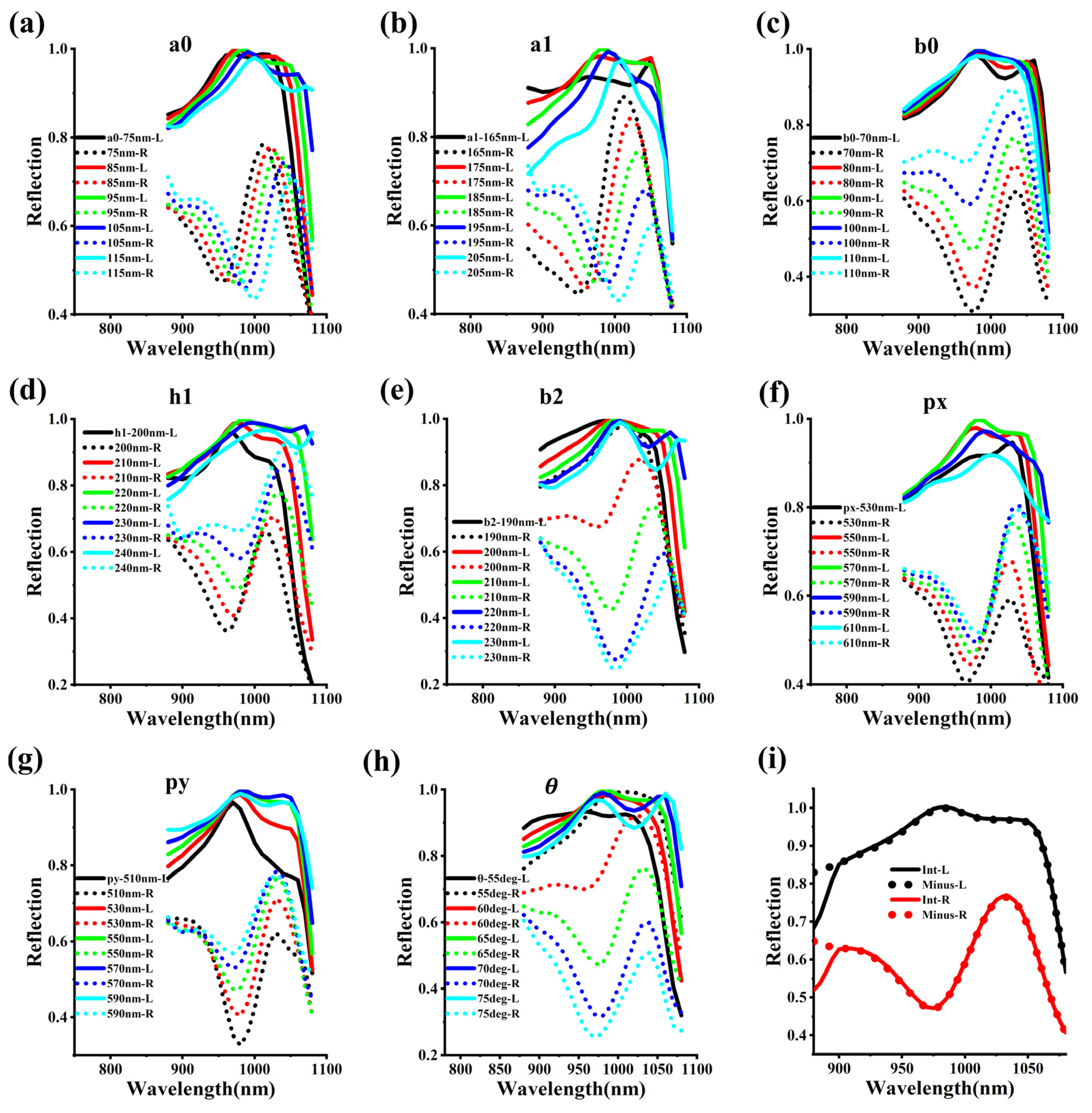
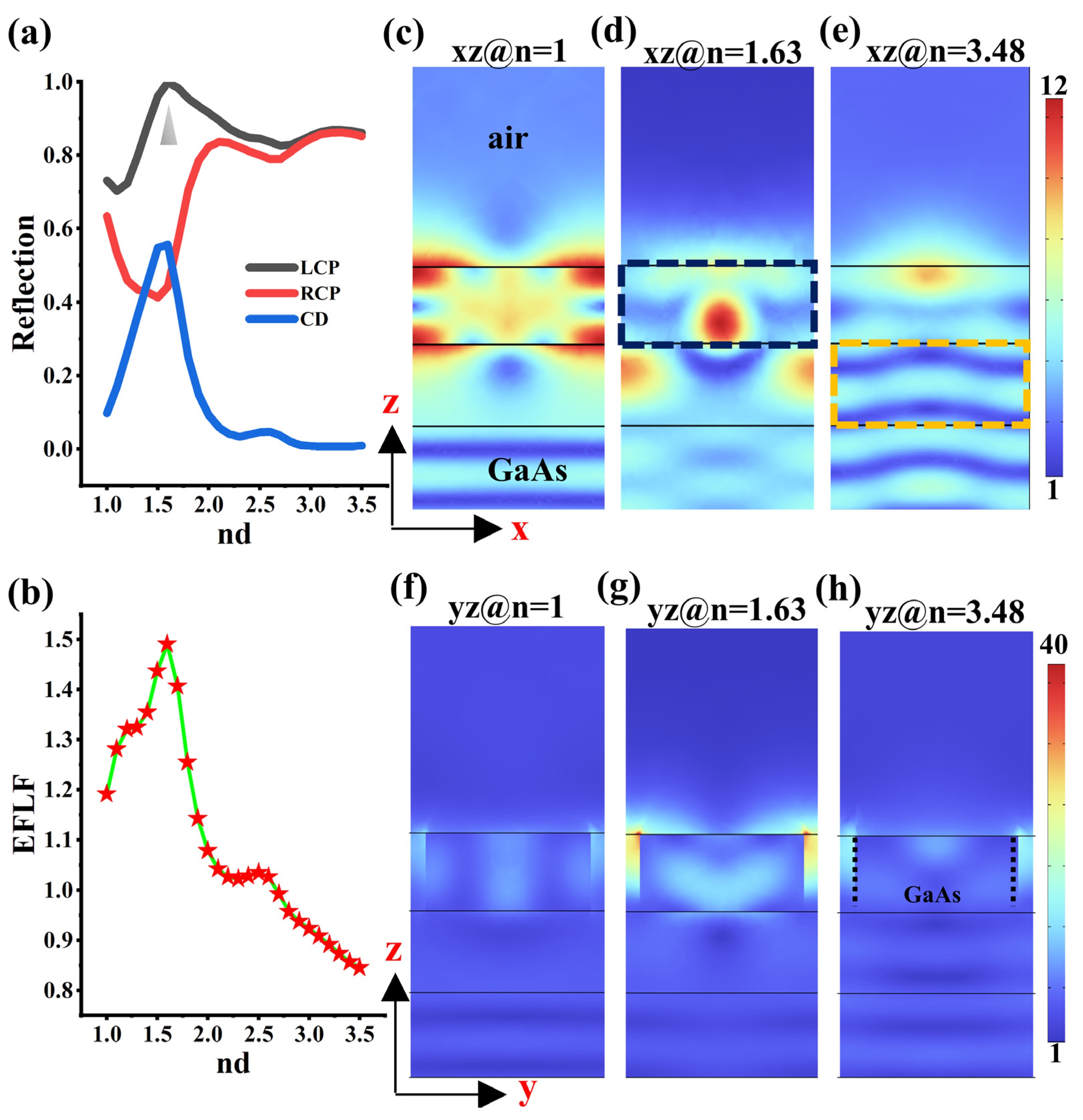
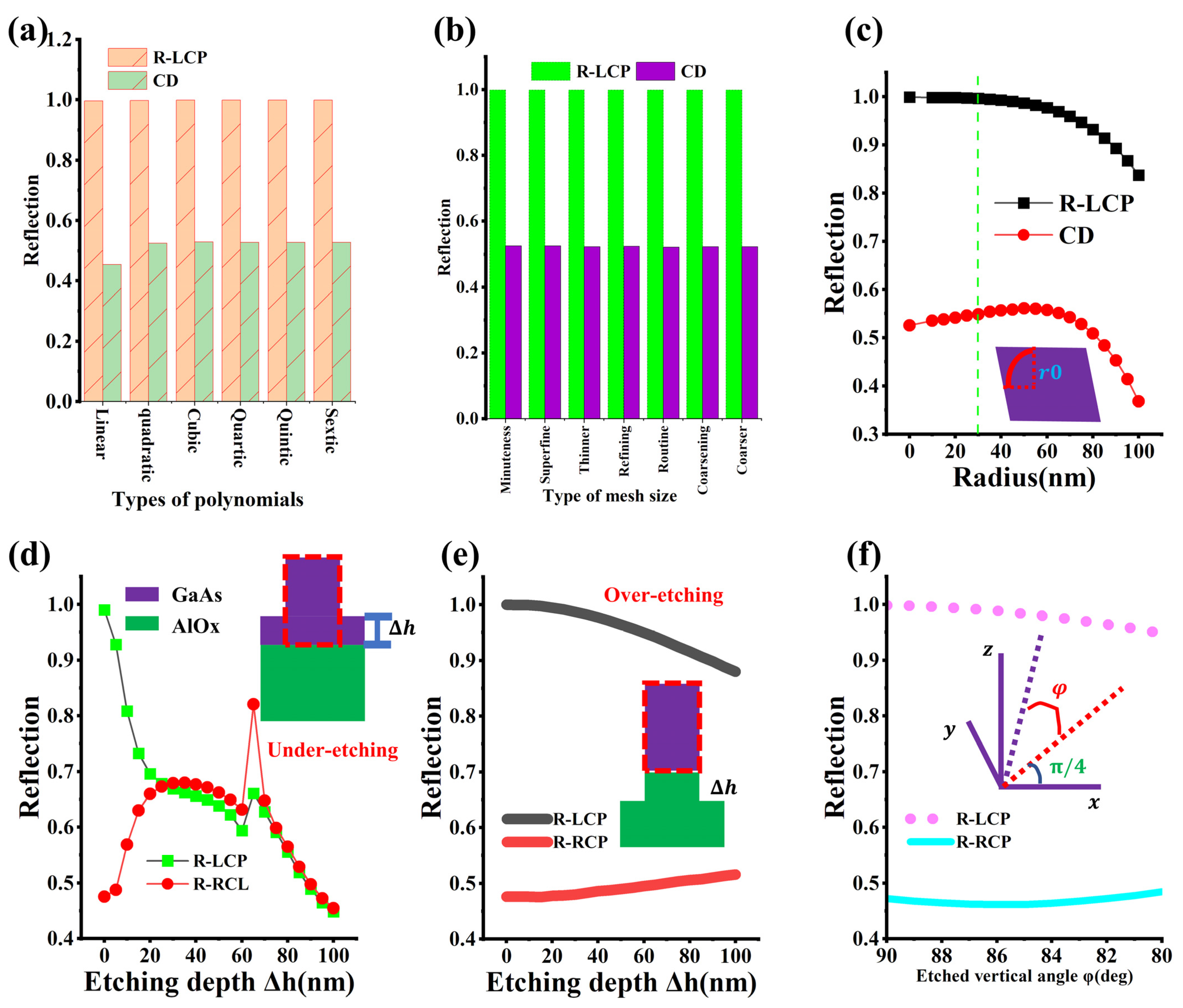
3.1. Scale Factor Analysis

The variation of dimensions directly affects the responsiveness of the metasurface to the specific wavelength, and the diversity of dimensions may also give rise to a wealth of information about spectral features. The analysis of the precise control of dimensions is also conducive to the enhancement of the stability of micro-photonic devices. Figure 3a demonstrates the effect of width a0 on the properties of chiral metasurfaces, where the reflection peaks of the CP are red-shifted with increasing width a0 and the CD peaks are gradually increased. As shown in Figure 3b, the reflection spectra of LCP do not seem to show a clear regularity for the change in width a1, but the reflection peaks of RCP exhibit a wide range of redshift characteristics with the increase in width a1. However, as shown in Figure 3c, the wavelength corresponding to the reflection peaks of the CP seem to be independent of the length b0, but the intensity of the reflection peaks of the RCP decreases significantly with the decrease in b0. Figure 3d,e demonstrate the effect of thickness h1 and length b2 on reflectivity, respectively. Near the operating wavelength of 980 nm, the change in reflectance of LCP is not very drastic, but the fluctuation range of reflectance of RCP exceeds 35%. Figure 3f shows that the reflection peak of LCP is blue-shifted and then red-shifted with the increase in period px, and the reflection spectrum of RCP shows only a weak red-shifting phenomenon. In addition, at the wavelength of 980 nm, Figure 3c,g are similar in that the intensity of the reflection peaks of the RCP both show a significant decreasing trend. Figure 3h demonstrates the dramatic effect of the angle of the parallelogram on the reflection spectrum. When the angle is less than 60 deg, the reflection peak of RCP shows the inversion phenomenon for the first time, i.e., the reflectivity of RCP exceeds that of LCP, which implies the complete disappearance of the CD phenomenon. Figure 3i illustrates the reflection spectrum of the optimized hypersurface in the 880 nm to 1080 nm band, which corresponds to the geometrical structure parameters of Figure 1b,c. Int in the legend corresponds to the integral form represented by Equation (2), while Minus corresponds to 1 minus the transmittance. The chiral metasurfaces exhibit significant CD phenomena throughout the band, with reflectances of 99.85% and 47.5% for LCP and RCP, respectively, at the operating wavelength of 980 nm. The fact that the solid and dashed lines do not coincide when the wavelength is less than 910 nm echoes the phenomenon that the imaginary part of the optical refractive index of GaAs in Figure 2b is not zero.

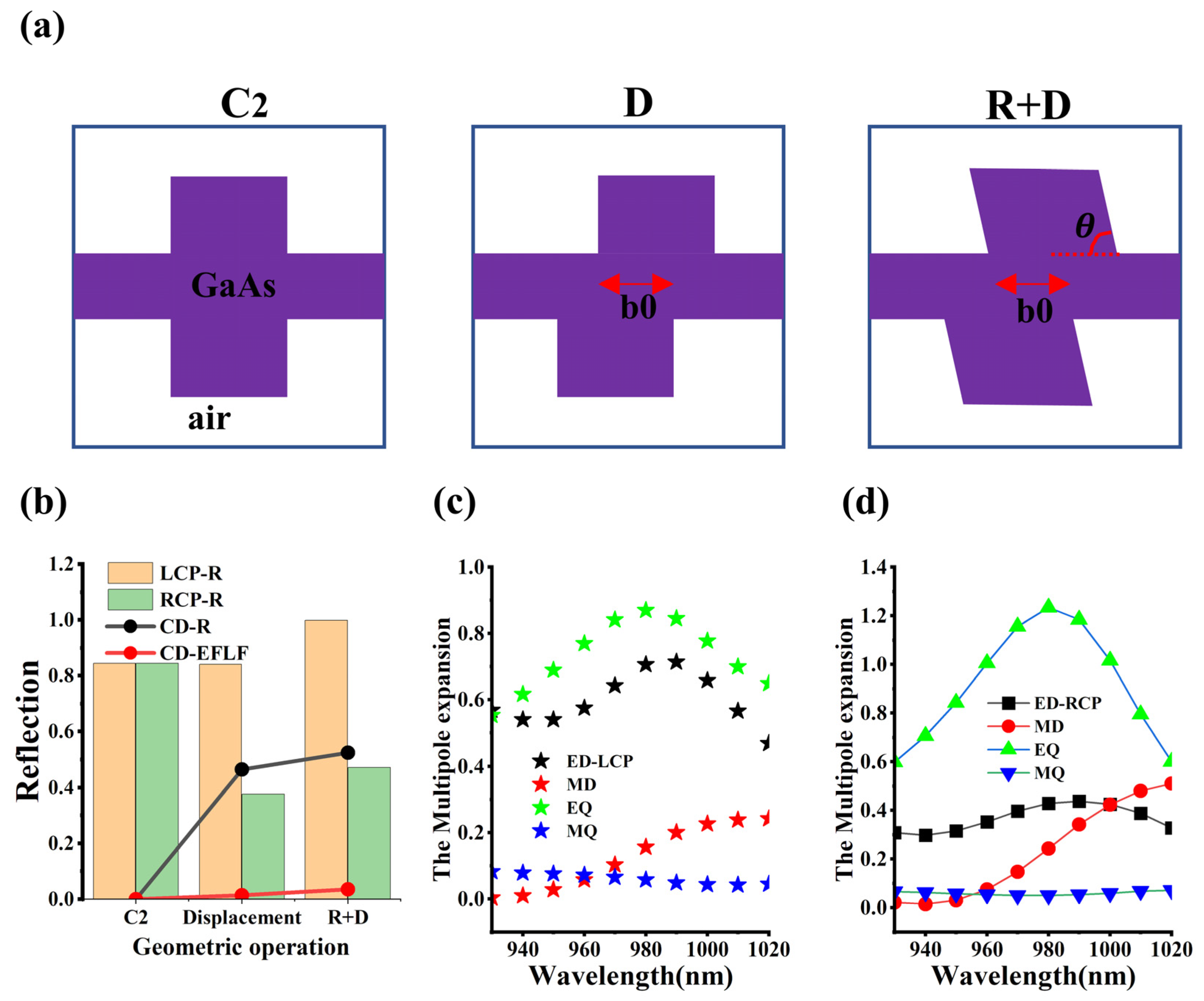
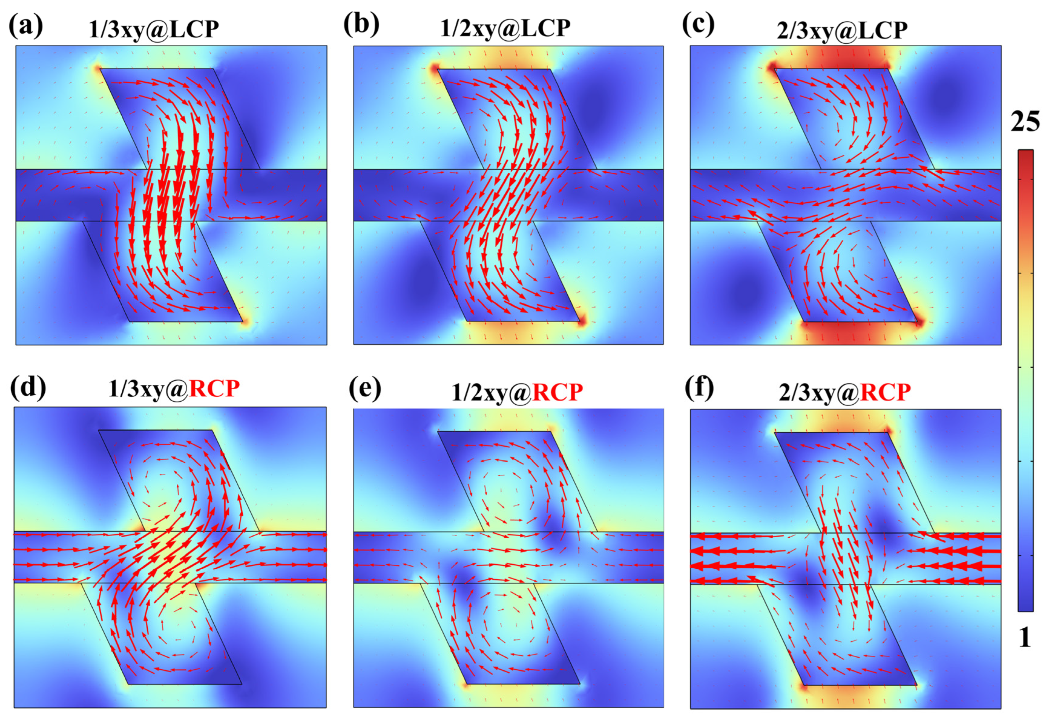
3.2. Chiral Evolution of Metasurfaces

High contrast grating is a special type of grating, which is usually composed of low-refractive-index material and high-refractive-index material spaced laterally by an air gap. This large refractive index contrast contributes to the enhancement of reflective properties of the grating, and the technology has been widely used in VCSELs. In addition, chiral hypersurfaces should be characterized by both ultra-high reflectivity and large CD. For the index of high reflectivity, a low-refractive-index AlOx film is designed underneath the GaAs microstructure pattern with the help of an oxidation process, and the light is reflected back to the incidence direction by forming a high contrast grating configuration. Figure 4a demonstrates the effect of the refractive index nd of the optical material in the region below the chiral GaAs metasurface on the reflectance and CD. When nd is 1.63, i.e., the optical material in the region below the metasurface is AlOx, the intensity of the reflection peak of the LCP is the largest, about 99.85%, and the CD increases and then decreases. The dramatic effect of nd on the reflectivity of the metasurface also suggests that the difference in the refractive indices is likely to be a major factor indeed in the increase in the reflectivity. Figure 4b illustrates the effect of the optical refractive index nd on the electric field localization factor (EFLF) inside the chiral metasurface, with the EFLF first increasing and then decreasing. Here, EFLF is | E | d V / | E 0 | d V ; E and E0 correspond to the electric field intensity inside the metasurface and the electric field intensity of the incident light, respectively. The range of integration is the volume occupied by the metasurface. To further explore the physical origin of the optical resonance modes inside the chiral metasurfaces, the electric field intensity distributions of the LCP under different nd conditions are shown in Figure 4c–h. For the xz cross-section, when nd = 1, the optical resonance exists mainly in the form of the radiative surface state, by which a significant fraction of the photon energy leaks into the air domain above. When nd = 1.6, a huge red ball appears inside the GaAs material, which refers to significant electric field localization effects. When nd = 3.48, the mode leakage also appears at the interface between the GaAs material and the air domain above. However, for the yz cross-section, only for nd = 1.63, a strong guided-mode resonance occurs, and it appears in a dielectric waveguide consisting of a GaAs–air–GaAs ternary system in the lateral direction. In addition, for the influence of the thickness of AlOx, please refer to the Supplementary Materials.
While the previous paragraph explored high reflectivity by analyzing the parameter of the refractive index contrast, this paragraph focuses more on investigating the optimization of the CD value. The chiral periodic array can generally be categorized into the 3D optical chiral and 2D optical chiral based on the mirror symmetry of the structure. Among them, the 2D optical chiral response refers to the case where the in-plane mirror symmetry is broken, in which the geometrical and material parameters of the chiral unit are just enough to couple with the incident CP photons, and thus, intrinsic chiral resonance occurs, realizing a highly controllable modulation of the circularly polarized photons. Figure 5a demonstrates the patterns of the unit cell of the metasurface with the C2 symmetry, after the displacement operation, and after double operation of the displacement and rotation, respectively, which clearly demonstrate the whole process of structural symmetry breaking, which refers to the process from zero chirality to large CD. Figure 5b illustrates the histograms of the reflection corresponding to the three unit-cell structures in Figure 5a. It is clear that both the reflectivity and the CD value of the LCP increase step by step, and the displacement operation and the rotation operation tend to modulate the CD value and the reflectivity, respectively. The size order of the EFLF under different operations remains consistent with that of the CD, and it seems to suggest that the near-field analysis of the metasurface may help to uncover the physical origin of the high CD phenomenon.
In addition, the multipole expansion is one of the widely used methods in dealing with the electromagnetic field problem, which can equate the radiative properties of an electromagnetic far field to a series of simple point sources, such as electric dipoles (EDs), magnetic dipoles (MDs), electric quadrupoles (EQs), and magnetic quadrupoles (MQs). The equations for the multipole expansion [30] can be expressed as, respectively:
E D = 1 i ω j d v
M D = 1 2 C ( r × j ) d v
E Q = 1 i ω [ r α j β + r β j α 2 3 ( r . j ) ] d v
M Q = 1 3 c [ ( r × j ) α r β + ( r × j ) β r α ] d v
Here, j and r refer to the equivalent current and distance vectors, respectively, and the markers α, β, and γ in the lower right corner refer to the three mutually orthogonal unit vectors. Figure 5c,d show the multipole expansion spectra of the chiral metasurface undergoing double manipulation upon the CP light incidence. For the LCP incident light at 980 nm, the chiral metasurface is under the combined control of the dark EQ mode and the bright ED mode. The terms “bright mode” or “dark mode” usually originate from the Fano resonance, and one of its typical features is an asymmetric spectrum, which coincides with the case of Figure 4a. For the case of the RCP incidence, the metasurface is almost exclusively controlled by the EQ mode, which exhibits some transmission function.
The distribution map of the electric field intensity is also one of the crucial means for investigating the physical mechanism of metasurfaces and possesses extensive application value in the research of optics and optoelectronics. Figure 6 presents the near-field plots of the xy cross-sections of chiral metasurfaces at a working wavelength of 980 nm. Here, the 1/3, 1/2, and 2/3 marks at the upper part of the picture respectively correspond to the scenarios where the height of the xy cross-section is 1/3, 1/2, and 2/3 of the thickness of the metasurface. Evidently, for all cases, nearly the majority of the energy is localized in the air gap formed by two adjacent GaAs unit cells along the y-axis direction, but the intensity in the LCP case is greater than that in the RCP case. Nevertheless, within the GaAs material, the case with a higher electric field intensity corresponds to RCP. Additionally, the red arrows in Figure 6 indicate the direction of the equivalent current, and the thickness of the arrows is proportional to the magnitude of the current. For the LCP incident case, if one examines the interior of the chiral metasurface along the direction of the current flow, it can be discovered that the equivalent current is composed of two semi-circles and it moves first clockwise and then counterclockwise. Then, for the RCP incident light, the equivalent current flows in the form of two entire circles from bottom to top, also first clockwise and then counterclockwise, but the current magnitude in the RCP case is smaller than that in the LCP case. Based on the theory in Reference [31], we conjecture that the intense optical coherent constructive interference between the LCP incident light and the far-field radiation generated by the equivalent current in Figure 6a–c occurs in the reflection domain, which is the direct cause of the LCP reflectivity approaching 100%. However, the RCP and its corresponding far-field radiation appear rather mediocre and do not yield an extreme amplitude enhancement at the transmission end. Table 1 displays the performance parameters of certain chiral metasurfaces placed within VCSELs over the recent three years. It can be discerned that the structure we designed, while fulfilling high efficiency, directly elevates the CD index from 2.1% to 52%, which constitutes an exhilarating breakthrough.

3.3. Error Analysis in Metasurfaces

This chapter primarily investigates the impact of potential errors introduced in the model and fabrication process on chiral metasurfaces. A superior optical simulation model ought to exhibit distinct convergence with regard to the polynomial components and mesh size within the finite element algorithm. Furthermore, the minimum geometrical size of the chiral metasurface is 90 nm for b0, and such minuscule lines necessitate realization through the electron beam lithography (EBL). EBL is a technique that employs a focused electron beam to pattern a substrate coated with photoresist. By means of EBL, the pattern in Figure 1c can be transferred onto the photoresist, and subsequently, dry etching is utilized to ultimately etch the chiral pattern onto the GaAs material. During the fabrication procedure, common etching manifestations such as etching fillets, etching tilt angles, over-etching, and under-etching arise due to diffraction stray light in lithography and non-zero isotropic etching components. Electromagnetic finite element algorithms can generally be categorized into several steps: derivation of the integral form of partial differential equations, discretization of the solution domain, selection of local processing units, assembly of the overall matrix, imposition of boundary conditions, and numerical solution of the matrix. Among them, in the local processing unit step, it is requisite to solve each element in the local matrix by employing the algebraic approach based on the distinct shape functions selected, which are typically polynomial functions. Figure 7a depicts the impact of diverse types of shape functions on the metasurface. The order of the polynomial is nearly independent of the reflectivity. When the order of the polynomial is greater than or equal to 2, the CD remains essentially unchanged. Furthermore, in the COMSOL software, the common options for mesh size typically encompass “coarser”, “coarsening”, “routine”, “refining”, “thinner”, “super-fine”, and “minuteness”. As illustrated in Figure 7b, the reflectivity and CD scarcely vary with the mesh size, which constitutes a robust validation for the correctness of the simulation outcomes. Figure 7c exhibits the influence of the radius of the etched fillet on the metasurface. The reflectivity of LCP declines as the radius of the fillet increases, while the CD initially increases and subsequently decreases. When the radius of the fillet is 30 nm, the reflectivity of LCP has already decreased to 99%. Figure 7d,e present the influence of the etching depth error Δ h . The red dashed-line frame in the inset corresponds to the ideal GaAs etching depth. For the over-etching phenomenon in Figure 7d, the performance of the chiral metasurface deteriorates significantly. When Δ h is 20 nm, the microstructure nearly loses its chirality. For the under-etching phenomenon in Figure 7e, the chirality decays gradually with the increase in Δ h . When Δ h is 100 nm, the CD is approximately 40%. Based on the data feedback in Figure 7d,e, when formally fabricating chiral metasurfaces, it is imperative to ensure that the etching type is under-etching initially. Secondly, a considerable number of dummy wafer processes should be conducted beforehand to explore the precise dry etching conditions, such as etching power, etching time, etching gas ratio, and the type of inert gas. Figure 7f indicates that the influence of the etching vertical angle on the chiral metasurface is also marginal.

4. Discussion

Using COMSOL software, we designed a chiral metasurface mirror suitable for direct integration into VCSELs. The mirror demonstrates 99.85% reflectivity for LCP light with a circular dichroism (CD) exceeding 50%. The near-perfect reflectivity is achieved through high contrast grating technology, implemented via an oxidation process that forms low-refractive-index AlOx beneath high-refractive-index GaAs layers. The significant CD value results from two geometric modifications—rotational and displacement operations—that break the unit cell’s spatial symmetry. This strong CD effect enables stable circularly polarized beam generation and shows promising potential for ultra-compact chiral light emitter applications.

Supplementary Materials

The following supporting information can be downloaded at: https://www.mdpi.com/article/10.3390/photonics12040341/s1, Figure S1: Front view of the COMSOL 3D simulation model; Figure S2: The influence of the thickness hs of the AlOx layer on the metasurface.

Author Contributions

Conceptualization, B.C. and Y.Z.; software, B.C.; validation, B.C. and Y.Z.; formal analysis, K.Z.; investigation, K.Z.; resources, G.S.; data curation, B.C.; writing—original draft preparation, B.C.; writing—review and editing, K.Z. and G.S.; visualization, Y.Z.; funding acquisition, G.S. All authors have read and agreed to the published version of the manuscript.

Funding

This research was funded by the Strategic Priority Research Program of the Chinese Academy of Sciences (grant no. XDB0980000).

Institutional Review Board Statement

The study did not involve humans or animals. The study did not require ethical approval.

Informed Consent Statement

The study did not involve humans.

Data Availability Statement

The raw data supporting the conclusions of this article will be made available by the authors on request.

Acknowledgments

The authors are grateful to Jietao Liu of Nankai University and Zengxuan Jiang of UCAS.

Conflicts of Interest

The authors declare no conflicts of interest.

References

  1. Hao, C.; Wang, G.; Chen, C.; Xu, J.; Xu, C.; Kuang, H.; Xu, L. Circularly Polarized Light-Enabled Chiral Nanomaterials: From Fabrication to Application. Nano-Micro Lett. 2023, 15, 39. [Google Scholar]
  2. Yeom, J.; Yeom, B.; Chan, H.; Smith, K.W.; Dominguez-Medina, S.; Bahng, J.H.; Zhao, G.; Chang, W.S.; Chang, S.J.; Chuvilin, A. Chiral Templating of Self-Assembling Nanostructures by Circularly Polarized Light. Nat. Mater. 2015, 14, 66–72. [Google Scholar] [CrossRef] [PubMed]
  3. Yan, T.; Li, F.; Qi, S.; Tian, J.; Tian, R.; Hou, J.; Luo, Q.; Dong, Z.; Xu, J.; Liu, J. Light-responsive vesicles for enantioselective release of chiral drugs prepared from a supra-amphiphilic M-helix. Chem. Commun. 2019, 56, 149–152. [Google Scholar] [CrossRef] [PubMed]
  4. Huck, N.P.; Jager, W.F.; De Lange, B.; Feringa, B.L. Dynamic control and amplification of molecular chirality by circular polarized light. Science 1996, 273, 1686–1688. [Google Scholar]
  5. Sun, M.; Qu, A.; Hao, C.; Wu, X.; Xu, L.; Xu, C.; Kuang, H. Chiral Upconversion Heterodimers for Quantitative Analysis and Bioimaging of Antibiotic-Resistant Bacteria In Vivo. Adv. Mater. 2018, 30, 1804241. [Google Scholar] [CrossRef]
  6. Wang, W.; Hao, C.; Sun, M.; Xu, L.; Wu, X.; Xu, C.; Kuang, H. Peptide Mediated Chiral Inorganic Nanomaterials for Combating Gram-Negative Bacteria. Adv. Funct. Mater. 2018, 28, 1805112. [Google Scholar]
  7. Hao, C.; Gao, R.; Li, Y.; Xu, L.; Sun, M.; Xu, C.; Kuang, H. Chiral Semiconductor Nanoparticles for Protein Catalysis and Profiling. Angew. Chem. Int. Ed. 2019, 58, 7371–7374. [Google Scholar]
  8. Zhao, X.; Xu, L.; Sun, M.; Ma, W.; Kuang, H. Tuning the interactions between chiral plasmonic films and livingcells. Nat. Commun. 2017, 8, 2007. [Google Scholar] [CrossRef]
  9. Wang, W.; Satyavolu, N.S.R.; Wu, Z.; Zhang, J.R.; Zhu, J.J.; Lu, Y. Near-Infrared Photothermally Activated DNAzyme-Gold Nanoshells for Imaging Metal Ions in Living Cells. Angew. Chem. 2017, 56, 6902–6906. [Google Scholar] [CrossRef]
  10. Gao, R.; Xu, L.; Hao, C.; Xu, C.; Kuang, H. Circular Polarized Light Activated Chiral Satellite Nanoprobes for the Imaging and Analysis of Multiple Metal Ions in Living Cells. Angew. Chem. 2019, 131, 3953–3957. [Google Scholar]
  11. Michalzik, R. VCSELs: Fundamentals, Technology and Applications of Vertical-Cavity Surface-Emitting Lasers; Springer: Berlin/Heidelberg, Germany, 2013. [Google Scholar]
  12. Ando, H.; Sogawa, T.; Gotoh, H. Photon-spin controlled lasing oscillation in surface-emitting lasers. Appl. Phys. Lett. 1998, 73, 566–568. [Google Scholar] [CrossRef]
  13. Iba, S.; Koh, S.; Ikeda, K.; Kawaguchi, H. Room temperature circularly polarized lasing in an optically spin injected vertical-cavity surface-emitting laser with (110) GaAs quantum wells. Appl. Phys. Lett. 2011, 98, 4516. [Google Scholar] [CrossRef]
  14. Uti, I.; Xu, G.; Lindemann, M.; Junior, P.E.F.; Gerhardt, N.C. Spin-Lasers: Spintronics Beyond Magnetoresistance. Solid State Commun. 2020, 316, 113949. [Google Scholar]
  15. Tanaka, Y.; Takano, H.; Kurokawa, T. Circular Polarization Resonator based on Cholesteric Liquid Crystal. In Proceedings of the Conference on Lasers & Electro-Optics, San Francisco, CA, USA, 16–21 May 2004; pp. 1062–1067. [Google Scholar]
  16. Zhou, Y.; Huang, Y.; Wu, S.T. Enhancing cholesteric liquid crystal laser performance using a cholesteric reflector. Opt. Express 2006, 14, 3906–3916. [Google Scholar] [CrossRef]
  17. Wang, C.T.; Lin, T.H. Polarization-tunable chiral nematic liquid crystal lasing. J. Appl. Phys. 2010, 107, 1707. [Google Scholar] [CrossRef]
  18. Goldstein, D. Polarized Light; CRC Press: Boca Raton, FL, USA, 2003. [Google Scholar]
  19. Kuznetsov, A.I.; Brongersma, M.L.; Yao, J.; Chen, M.K.; Levy, U.; Tsai, D.P.; Zheludev, N.I.; Faraon, A.; Arbabi, A.; Yu, N. Roadmap for Optical Metasurfaces. Appl. Phys. Lett. 2024, 124, 260701. [Google Scholar]
  20. Kim, J.; Kim, W.; Oh, D.K.; Kang, H.; Kim, H.; Badloe, T.; Kim, S.; Park, C.; Choi, H.; Lee, H. One-step printable platform for high-efficiency metasurfaces down to the deep-ultraviolet region. Light Sci. Appl. 2023, 12, 68. [Google Scholar] [CrossRef]
  21. Saha, S.; Segal, O.; Fruhling, C.; Lustig, E.; Segev, M.; Boltasseva, A.; Shalaev, V.M. Photonic time crystals: A materials perspective [Invited]. Opt. Express 2023, 31, 8267–8273. [Google Scholar] [CrossRef]
  22. Vabishchevich, P.; Kivshar, Y. Nonlinear photonics with metasurfaces. Photonics Res. 2023, 11, 122–136. [Google Scholar] [CrossRef]
  23. Wen, D.; Meng, J.; Cadusch, J.J.; Crozier, K.B. VCSELs with On-Facet Metasurfaces for Polarization State Generation and Detection. Adv. Opt. Mater. 2021, 9, 2001780. [Google Scholar]
  24. Kulakovskii, V.D.; Lobanov, S.V.; Tikhodeev, S.G.; Hoefling, S.; Weiss, T. Circularly polarized lasing in chiral modulated semiconductor microcavity with GaAs quantum wells. Appl. Phys. Lett. 2016, 109, 171106. [Google Scholar]
  25. Maksimov, A.A.; Filatov, E.V.; Tartakovskii, I.I.; Kulakovskii, V.D.; Tikhodeev, S.G.; Schneider, C.; Höfling, S. Circularly Polarized Laser Emission from an Electrically Pumped Chiral Microcavity. Phys. Rev. Appl. 2022, 17, L021001. [Google Scholar] [CrossRef]
  26. Zhang, X.; Liu, Y.; Han, J.; Kivshar, Y.; Song, Q. Chiral emission from resonant metasurfaces. Science 2022, 377, 1215–1218. [Google Scholar] [PubMed]
  27. Jia, X.; Kapraun, J.; Wang, J.; Qi, J.; Ji, Y.; Chang-Hasnain, C. Metasurface reflector enables room-temperature circularly polarized emission from VCSEL. Optica 2023, 10, 1093–1099. [Google Scholar]
  28. Papatryfonos, K.; Angelova, T.; Brimont, A.; Reid, B.; Guldin, S.; Smith, P.R.; Tang, M.; Li, K.; Seeds, A.J.; Liu, H.; et al. Refractive indices of MBE-grown AlxGa(1−x)As ternary alloys in the transparent wavelength region. AIP Adv. 2021, 11, 025327. [Google Scholar] [CrossRef]
  29. Jensen, F.; Lavrinenko, A.V.; Malureanu, R.; Zhukovsky, S.V.; Andryieuski, A.; Takayama, O.; Shkondin, E. Experimental Demonstration of Effective Medium Approximation Breakdown in Deeply Subwavelength All-Dielectric Multilayers. Phys. Rev. Lett. 2015, 115, 177402. [Google Scholar]
  30. Yang, B.; Liu, W.; Li, Z.; Cheng, H.; Choi, D.Y.; Chen, S.; Tian, J. Ultrahighly Saturated Structural Colors Enhanced by Multipolar-Modulated Metasurfaces. Nano Lett. 2019, 19, 4221–4228. [Google Scholar]
  31. Gansel, J.K.; Thiel, M.; Rill, M.S.; Decker, M.; Bade, K.; Saile, V.; von Freymann, G.; Linden, S.; Wegener, M. Gold Helix Photonic Metamaterial as Broadband Circular Polarizer. Science 2009, 325, 1513–1515. [Google Scholar] [CrossRef]
  32. Cheng, B.; Jiang, B.; Zou, Y.; Song, G. Ultrahigh-Reflectivity Circularly Polarized Mirrors Based on the High-Contrast Subwavelength Chiral Metasurface. Photonics 2024, 11, 923. [Google Scholar] [CrossRef]
Figure 1. (a) The chiral metasurface reflectors in VCSELs, and the system above the oxide layer is the configuration of the chiral metasurface. (b) Front view of the chiral metasurface. The h1 = 220 nm, hs = 230 nm. (c) Top view of the chiral metasurface. The px = 570 nm, py = 550 nm, a0 = 95 nm, a1 = 185 nm, b0 = 90 nm, b2 = 210 nm, θ = 65 deg.
Photonics 12 00341 g001
Figure 2. (a) The optical simulation model decomposition diagram based on the finite element algorithm. (b) The refractive index of the GaAs in the wavelength range of 0.7 µm to 1.3 µm. The black arrow pointing to the left indicates that the vertical axis of the corresponding curve is on the left.
Photonics 12 00341 g002
Figure 3. The scaling effects of geometric parameters in chiral metasurface. (ah): The influence of geometrical dimensions a0, a1, b0, h1, b2, px, py and θ on the spectral properties of metasurfaces. (i): The reflection spectrum of the optimized metasurface. The titles of the subplots correspond to the metasurface parameters. L and R in the legend, respectively, correspond to the cases where the incident light is LCP and RCP. Additionally, dashed lines and solid lines, respectively, correspond to RCP and LCP.
Photonics 12 00341 g003
Figure 4. (a) The effect of refractive index changes in the surrounding medium on chiral reflective microdevices. (b) EFLF of the chiral metasurface for different refractive index cases. The metasurface corresponding to (b) is the optimized version, and when analyzing the substrate refractive index nd, the hs remains unchanged. (ch) Electric field distributions on the chiral metasurface in some refractive index cases. The black dashed box is the boundary of the GaAs material in the metasurface and the orange dashed box is the boundary of the low-refractive material.
Photonics 12 00341 g004
Figure 5. (a) The chiral evolutionary paths for the unit cell in the metasurface reflector, involving the displacement operation and the rotation operation. (b) Reflectance after some geometric manipulations at an operating wavelength of 980 nm. (c,d) Multipole expansion of the chiral hypersurface mirror in the LCP and RCP cases.
Photonics 12 00341 g005
Figure 6. Near-field profiles on xy cross-sections of the chiral metasurface at different heights at the 980 nm operating wavelength. The “1/3”, “1/2”, and “2/3” above the picture respectively represent the cross-sections at 1/3, 1/2, and 2/3 of the thickness of the metasurface. (ac): The case of LCP incidence. (df): The case of RCP incidence. The red arrow represents the direction of the equivalent current.
Photonics 12 00341 g006
Figure 7. The influence of the type of polynomials in the optical model, the type of maximum grid size, the radius of the fillet, the error in the etching depth, and the etched vertical angle on the chiral metasurface reflector. (a): The type of polynomials in the optical model. (b): The type of maximum grid size. (c): The radius of the fillet. (d): Under-etching. (e): Over-etching. (f): The etched vertical angle. In (f), the three mutually orthogonal purple solid lines denote the three edge lengths corresponding to any vertex within the cubic block, and the red dashed line bisects the xy plane. Upon the conclusion of the etching process, the line that is more likely to emerge is the purple dashed one rather than the ideal z. The etching vertical angle φ is defined as the angle constituted by the purple dashed line and the red dashed line.
Photonics 12 00341 g007
Table 1. Comparison of some chiral metasurfaces in VCSELs.
Structure DesignDate of PublicationCenter WavelengthEfficiencyCD
Gammadion [27]August 2023940 nm~99.8%0.75%
Gammadion [27]August 2023940 nm98.4%0.2%
Z-shaped hole [32]September 2024980 nm99.9%2.1%
This work 980 nm99.85%52%
Disclaimer/Publisher’s Note: The statements, opinions and data contained in all publications are solely those of the individual author(s) and contributor(s) and not of MDPI and/or the editor(s). MDPI and/or the editor(s) disclaim responsibility for any injury to people or property resulting from any ideas, methods, instructions or products referred to in the content.

