Abstract
Rapid full-field surface topography measurement for large-scale wafers remains challenging due to limitations in speed, system complexity, and scalability. This work presents a interferometric system based on thin-film interference for high-precision wafer profiling. An optical flat serves as the reference surface, forming a parallel air-gap structure with the wafer under test. A large-aperture collimated beam is introduced via an off-axis parabolic mirror to generate high-contrast interference fringes across the entire field of view. Once the wafer is fully illuminated, topographic information is directly extracted from the fringe pattern. Comparative measurements with a commercial interferometer show relative deviations below in bow and warp, confirming the system’s accuracy and stability. With its simple optical layout, low cost, and robust performance, the proposed method shows strong potential for industrial applications in wafer inspection and online surface monitoring.
1. Introduction
Wafers are fundamental substrates in semiconductor manufacturing, and even subtle variations in their surface topography can significantly affect critical processes such as photolithography and etching, ultimately impacting device performance and production yield [1,2]. With the ongoing miniaturization of integrated circuit features and the increasing diameter of wafers, accurate and efficient surface topography characterization has become essential for ensuring quality and functionality in advanced semiconductor devices [3]. This evolving demand places stringent requirements on metrology systems, which must achieve micrometer- or submicrometer-level precision over areas spanning several hundred millimeters—posing considerable challenges for conventional measurement techniques [4,5]. As a result, the development of high-precision, high-efficiency, full-field surface measurement technologies for large-scale wafers holds both significant research value and practical importance for industrial implementation [6].
Conventional methods for measuring wafer topography are typically classified into contact-based and optical approaches. Contact profilometers provide good measurement accuracy but are hindered by slow scanning speeds and the risk of mechanical damage to delicate wafer surfaces [7]. Atomic force microscopy (AFM), while capable of nanometer-scale resolution, suffers from limited measurement range and low throughput, making it unsuitable for full-field inspection of large wafers [8]. These limitations have shifted focus toward optical metrology, which offers non-contact, high-speed, and high-precision measurement capabilities suitable for industrial environments [9].
Several optical methods have been developed for three-dimensional surface topography measurement, including laser confocal microscopy [10], digital holography [11], structured light projection [12], and optical interferometry [13]. Laser confocal systems offer excellent vertical resolution and immunity to stray light, yet their point-by-point scanning mechanism restricts measurement efficiency. Digital holography enables rapid, full-field acquisition with high spatial resolution but is vulnerable to phase noise and system complexity, particularly when employing multi-wavelength configurations. Structured light projection supports large-area measurements but often lacks the vertical resolution required for accurate wafer surface characterization. Among these techniques, optical interferometry stands out due to its high vertical accuracy, fast imaging speed, simple system architecture, and strong environmental stability [14]. Recent developments in interferometric techniques have significantly advanced wafer metrology, with innovations such as vertical-state wavelength-tuned interferometry enabling distortion-free wafer profiling [15], single-shot dual-wavelength configurations overcoming phase ambiguity [16], and adaptive scanning strategies improving efficiency for high-aspect-ratio structures [17]. However, achieving rapid and precise full-field measurements over large-scale wafer areas remains a critical technical challenge for interferometric systems [18,19].
To overcome these challenges, we propose a thin-film interference-based measurement system designed specifically for the rapid and accurate characterization of large-scale wafer surface topography. The system utilizes an optical flat as the reference surface and employs an off-axis parabolic mirror to introduce a large-aperture collimated beam, which generates high-contrast interference fringes across the wafer surface. For accurate and efficient data extraction, we develop an optimized interferogram processing workflow incorporating fringe skeleton extraction and a novel fringe order determination algorithm suitable for complex fringe patterns. The surface profile reconstruction is achieved using polynomial fitting, enabling full-field topography mapping. Experimental validation on both 2-inch and 4-inch wafers demonstrates the system’s high accuracy, stability, and scalability, confirming its potential as a practical and robust solution for in-situ, high-precision wafer surface metrology in semiconductor manufacturing.
2. Measurement Principle
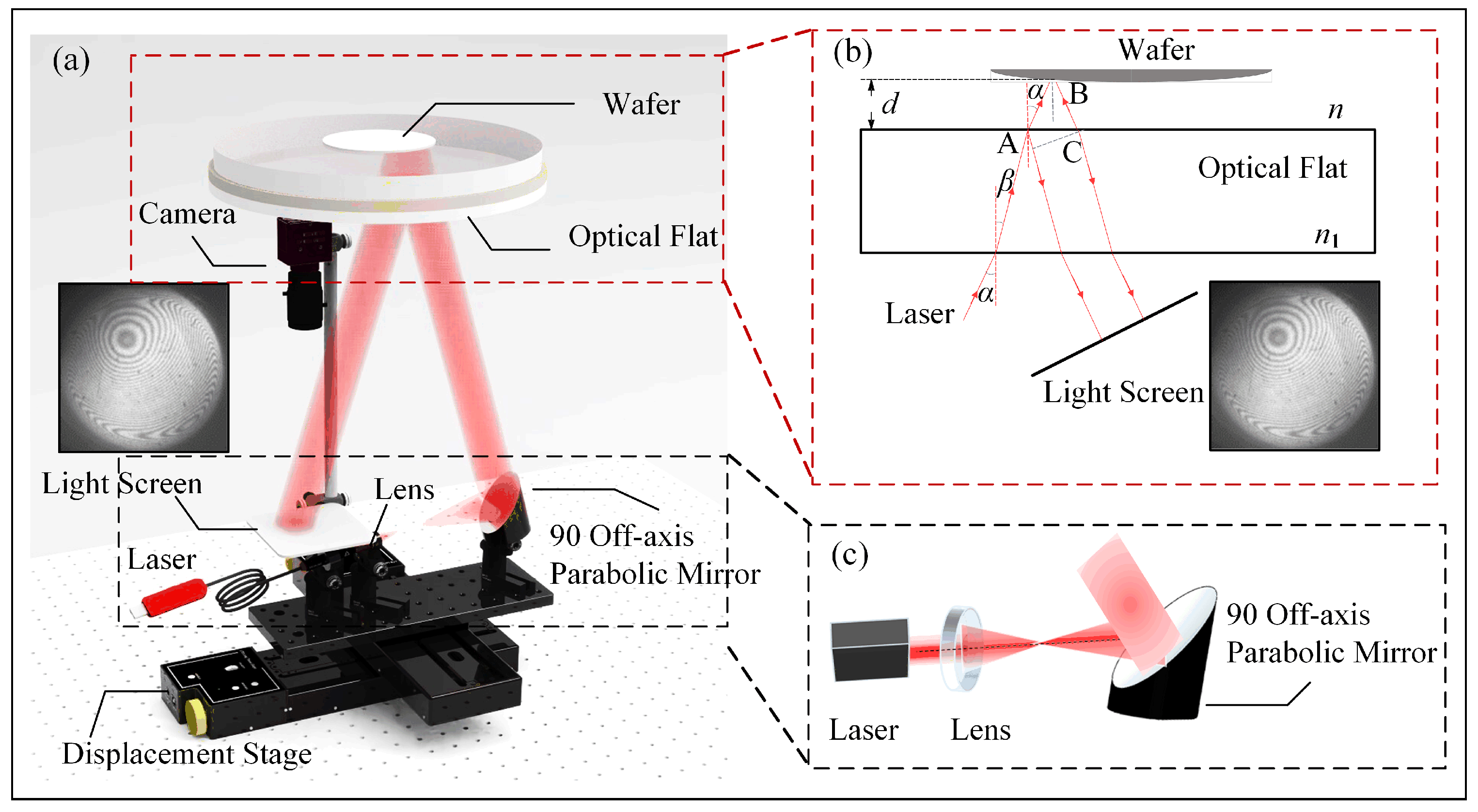
The measurement system primarily consists of a laser source, a beam-expanding lens, an off-axis parabolic mirror, an optical flat, the wafer under test, a precision displacement stage, a camera, and a computer processing unit. The overall working principle is illustrated in Figure 1. A laser is used as the coherent illumination source. The emitted laser beam is first expanded by the beam-expanding lens and then collimated by the off-axis parabolic mirror to form a large-aperture collimated beam. The beam diameter can be flexibly configured according to the size of the wafer to ensure uniform illumination over the entire wafer surface.
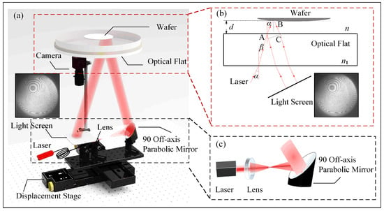
Figure 1.
Schematic diagram of measurement system (a) System schematic, (b) Thin-film interference principle, (c) Off-axis parabolic mirror-based beam expansion and collimation module.
During the measurement process, the optical flat functions as the reference plane, while the wafer under test is placed slightly above it, forming a parallel air-gap thin-film structure between the two surfaces. According to the principle of thin-film interference, variations in the thickness of this air gap correspond directly to local height differences on the wafer surface. These thickness differences cause phase shifts in the reflected light beams from the wafer and the reference surface, resulting in interference fringes with spatially varying intensity. In other words, topographic undulations on the wafer modulate the phase difference between the interfering beams, producing a fringe pattern that encodes the surface height information. To capture the interference fringes, the system employs a mirror-type projection screen, onto which the interference pattern is reflected and then imaged by the camera in real time. This indirect imaging configuration offers several advantages: it attenuates direct laser intensity to protect the camera, decouples the imaging axis from the measurement axis to simplify system integration and allow future extensions, and improves optical compatibility with the camera lens to ensure uniform fringe contrast and clarity. This design enhances the system’s overall robustness and scalability. To suppress the influence of ambient light on fringe visibility, a black light-shielding curtain is used to isolate the setup from external illumination. The captured alternating bright and dark fringes contain detailed information about the wafer’s surface profile, which is subsequently analyzed by the computer to reconstruct the topography quantitatively.
As illustrated in Figure 1b, a monochromatic beam with wavelength is incident from air (refractive index n) onto the surface of the optical flat (refractive index ) at an angle of incidence , which is typically set between 15° and 20°. The beam is refracted at an angle upon entering the optical flat, and the relationship between and follows Snell’s Law:
Since an air film gap with a thickness d is formed between the wafer’s measured surface and the optical flat’s reference surface, the incident light is reflected at the wafer’s measured surface and the optical flat’s reference surface, respectively. According to the geometric configuration shown in Figure 1b, the geometric optical path difference between the two reflected beams, which gives rise to interference, is expressed as:
Given that the air gap d is typically very small, the path lengths of , , and can be approximated using trigonometric relations:
Substituting these approximations into Equation (2), and considering the half-wave phase loss due to reflection, the total optical path difference can be simplified to:
According to the principle of optical interference, constructive or destructive interference occurs depending on whether the optical path difference satisfies the following conditions:
Points on the wafer surface that lie along the same fringe (i.e., share the same fringe order k) correspond to equal air-gap thickness and therefore represent equal height levels. Combining Equations (4) and (5), the surface height difference between adjacent bright (or dark) fringes is given by:
This expression shows that the vertical spacing between adjacent interference fringes reflects the local surface height variation on the wafer, and is determined by the incident wavelength, incidence angle, and refractive indices of the media. By assigning a reference height to the zero-order fringe and sequentially determining the fringe order across the pattern, the relative height of each fringe can be calculated. In this way, the full-field surface topography of the wafer can be reconstructed from the interference fringe distribution.
3. Surface Topography Reconstruction
3.1. Fringe Order Determination
Based on the measurement principle described above, interference fringe patterns that encode the wafer’s surface topography can be acquired through the imaging system. To reconstruct the three-dimensional surface profile, it is essential to accurately determine the order of each fringe, which represents a relative height level within the optical path. This process requires extracting structured fringe information from the raw image and translating it into quantitative topography. Given the complexity, noise, and morphological variability of real fringe patterns, a robust and well-structured image processing workflow is critical for reliable order assignment.
The first stage of fringe analysis involves segmenting the fringe regions from the background. Global thresholding often fails under uneven illumination or weak contrast, which are common in full-field interferograms. Therefore, a local adaptive thresholding algorithm, specifically the Niblack method [20], is employed to improve segmentation robustness. This method computes a unique threshold for each pixel based on the local mean and standard deviation of grayscale values within a defined neighborhood window, using the formula , where k is typically set to −0.2. This approach effectively adapts to varying fringe intensities and suppresses noise, ensuring that both bright and dim fringes are correctly segmented.
After binarization, a thinning operation is performed to extract the centerlines of all fringe regions. The Zhang–Suen algorithm [21]) is selected for this task due to its ability to iteratively remove peripheral pixels while preserving the structural connectivity of the binary image. The thinning process ensures that the width of each fringe is reduced to a single pixel, simplifying subsequent morphological analysis. In addition, morphological filters such as spur and bridge removal are applied to break spurious connections (e.g., short branches or H-bridges) and to improve skeleton continuity. The resulting fringe skeletons preserve the topological structure and spatial trajectory of the original fringes, while greatly reducing data redundancy.
With the skeletons extracted, each fringe is identified as a connected domain. A crucial step is to assign a fringe order to each segment relative to a designated zero-order fringe, which serves as the reference height. Traditional traversal-based methods are often sensitive to scanning direction, image rotation, and fringe grouping, which can result in inconsistent or inaccurate order labeling, particularly in images that contain a mixture of open and closed fringe types.
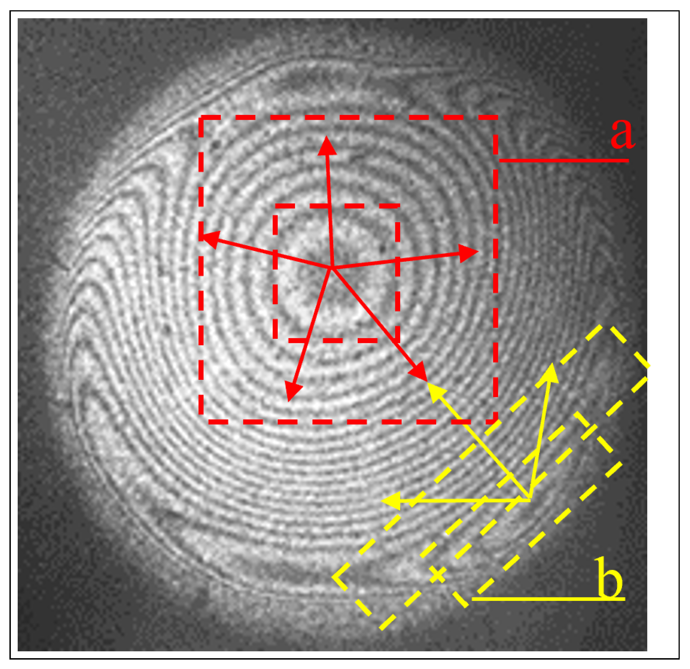
To overcome these challenges, this study introduces a classification method based on image-connected domains. The approach evaluates the morphological characteristics of each connected region to enable robust and rotation-invariant fringe order assignment. In particular, the aspect ratio of the minimum bounding rectangle is employed as the primary criterion to distinguish between closed and non-closed fringes. Closed fringes, such as those resembling Newton rings, typically display low aspect ratios due to their isotropic geometry, whereas non-closed fringes, including linear or arc-shaped patterns, tend to exhibit higher aspect ratios resulting from their elongated structure.
These characteristics are illustrated in Figure 2, which shows actual examples of fringe classification. In the image, region ‘a’ represents a group of nearly circular closed fringes with low aspect ratios, while region ‘b’ highlights elongated, non-closed linear fringes associated with wafer warpage. The figure demonstrates how morphological features can effectively distinguish fringe types for order assignment.
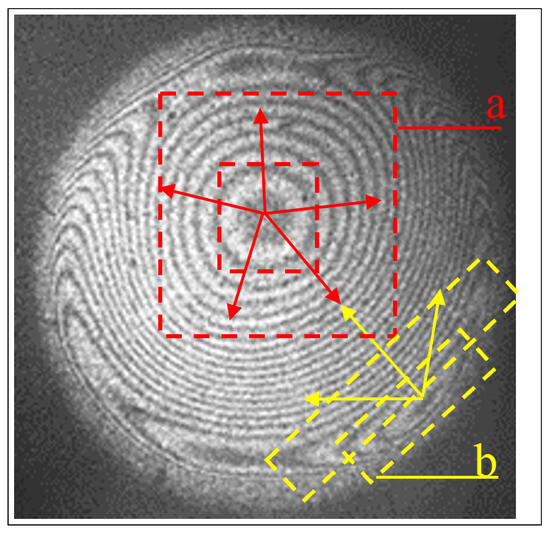
Figure 2.
Grading of actually acquired interference images.
The region area is used as an auxiliary feature to further distinguish fringe instances within each group. For closed fringes, segments are ranked by ascending area, based on the assumption that smaller fringes correspond to lower fringe orders. For non-closed fringes, area and spatial continuity are jointly considered. In cases where non-closed fringes resemble closed loops and deviate from expected trends, an adaptive aspect ratio threshold is introduced to reclassify such segments correctly. This improves the robustness of the classification process and ensures accurate fringe sequencing.
Following classification and ordering, the optical path difference between each fringe and the reference is calculated based on fringe order and known system parameters. This difference is then mapped to relative surface height using the interference equation described in Section 2. The output is a sparse but structured height map aligned with the fringe skeletons, which serves as the input for the subsequent surface reconstruction process.
In summary, the fringe order determination pipeline uses adaptive thresholding, skeletonisation, morphological classification and image-connected domain-based ranking to provide an automated, accurate and robust method of analysing complex interference patterns.
3.2. Surface Profile Reconstruction
Following fringe order determination, the relative height differences corresponding to bright fringes of different orders can be calculated based on the thin-film interference principle, using the zero-order fringe as the reference plane. This process yields discrete height data along the skeleton lines of the interference fringes. However, since these skeletons are derived from binarized and thinned images, the resulting data only occupy a subset of pixels in the image, leaving extensive background regions unassigned. Applying global surface fitting directly, or simply excluding zero-value regions prior to fitting, typically leads to discontinuous surfaces that lack physical consistency.
To address this limitation, a surface reconstruction method combining skeleton-based interpolation and polynomial surface fitting [22] is proposed. The workflow of the algorithm is shown in Figure 3, and includes the following key steps:
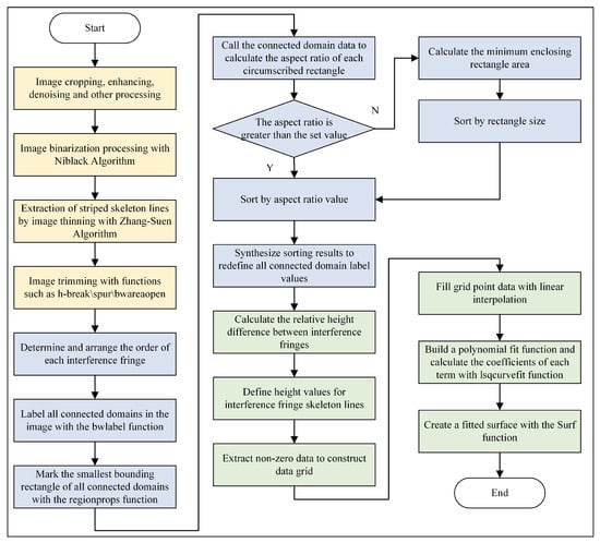
Figure 3.
Algorithm flow chart of surface profile reconstruction.
(1) Skeleton Point Extraction and Grid Construction: Grayscale values and their corresponding two-dimensional spatial coordinates (X, Y) are extracted from all non-zero pixels in the interference image and stored in three separate vectors. A 2D spatial grid covering the full image domain is then generated based on the coordinate ranges.
(2) Interpolation-Based Expansion: Known height values along the fringe skeletons are mapped onto the corresponding grid points. Linear interpolation is applied to estimate height values for the unassigned grid nodes, resulting in a dense, quasi-continuous dataset of surface points.
(3) Surface Fitting: Using the interpolated height data, a polynomial surface model is constructed. A parametric array containing the coefficients of polynomial terms is generated, and the optimal model parameters are determined via least-squares fitting. This yields a smooth, continuous surface that accurately represents the wafer’s topography.
This reconstruction approach maintains the physical meaning of the fringe order distribution while significantly improving the smoothness and continuity of the final surface. It is particularly well-suited for dense fringe patterns in large-scale wafer interferograms, enabling accurate and reliable topography reconstruction.
4. Experiment Setup
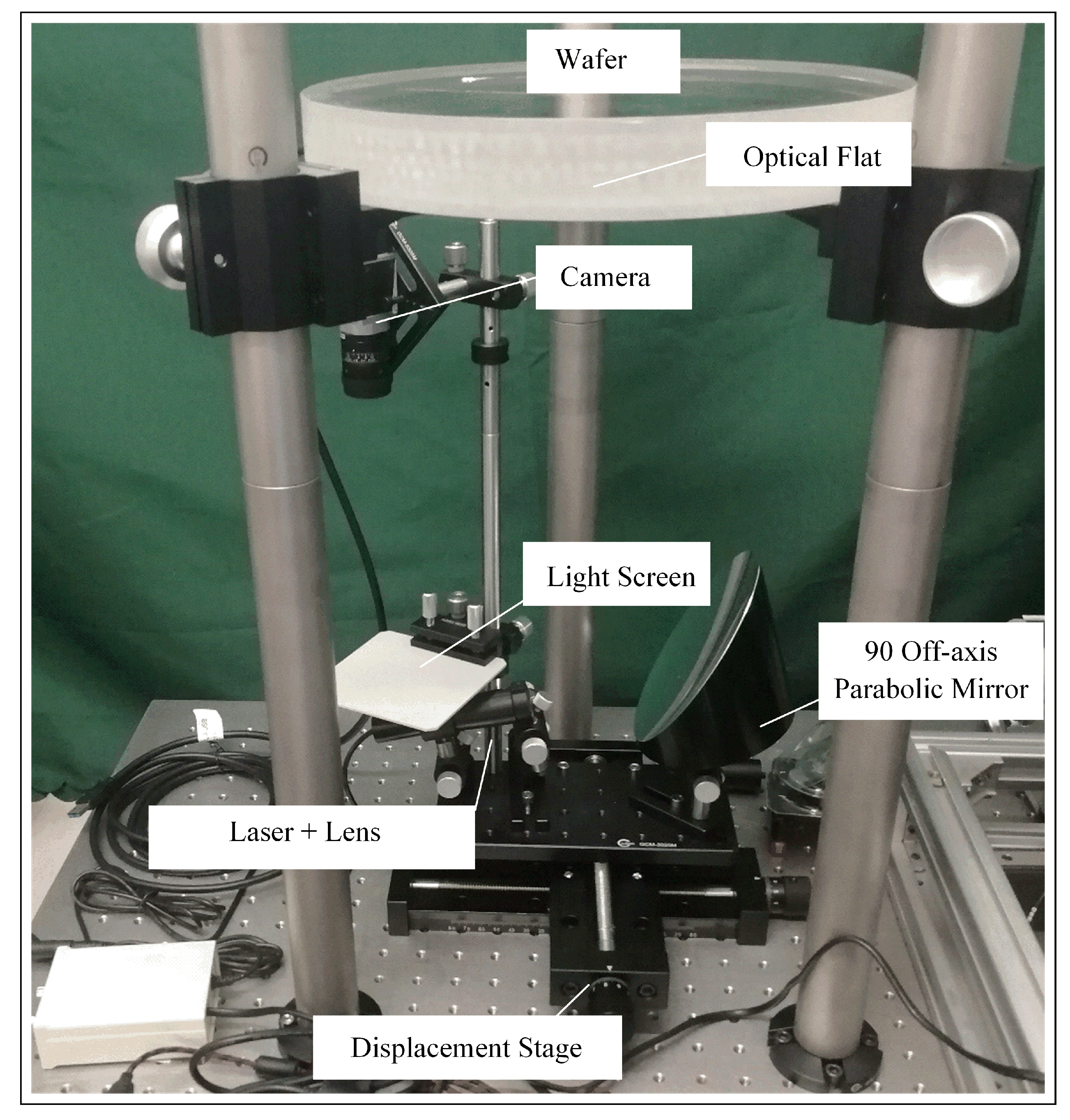
To verify the feasibility and stability of the proposed full-field rapid surface topography measurement scheme for large-scale wafers, a physical experimental platform was constructed, as shown in Figure 4.
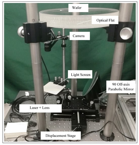
Figure 4.
Wafer Surface Topography Measurement System.
The system was developed through systematic configuration and parameter optimization of its core components. A laser module (E635-2-3-20) with a central wavelength of , output power of , and beam diameter of was used as the coherent light source. Its high wavelength stability and spatial coherence satisfy the precision requirements of interferometric measurements. A high-precision optical flat with a diameter of and thickness of served as the reference surface, featuring surface flatness of (upper face) and (lower face), and a parallelism of , providing a stable and accurate interference reference plane.
A 4-inch off-axis parabolic mirror with a deviation angle of and a focal length of was employed to convert the expanded laser beam into a collimated beam with a diameter of approximately , enabling uniform illumination of both 2-inch and 4-inch wafers. For image acquisition, the a2A2590-60BAS Basler ace 2 R camera (Basler AG, Ahrensburg, Germany) with a resolution of pixels, pixel size of , and a frame rate of was utilized to provide high-definition imaging with excellent dynamic response. The imaging system was completed with a Basler Lens C125-0618-5M-P (Basler AG, Ahrensburg, Germany) featuring a focal length of , which offers a field of view of at a working distance of , meeting the full-field imaging requirements for localized wafer regions. Overall, the system demonstrates a compact and integrated structure with well-matched optical and mechanical parameters, achieving a balance between high-precision interferometric imaging and practical engineering implementation. This platform establishes a reliable foundation for subsequent interference image processing and wafer surface topography reconstruction.
5. Results and Discussion
To evaluate the reliability and accuracy of the proposed interferometric measurement method, two single-side polished silicon wafers of different sizes were selected as experimental samples. Sample 1 was a 2-inch wafer, and Sample 2 was a 4-inch wafer, both featuring single-side polished surfaces whose polished sides were measured in the experiments. A commercially available interferometric instrument with a similar working principle, namely Tropel Flatmaster MSP 150 (Corning, New York, NY, USA), was employed as the reference system for performance benchmarking. This device utilizes step-by-step laser interferometry and enables the measurement of surface parameters such as flatness, thickness, and warpage for wafers up to 6 inches in diameter. Its specifications include a measurement accuracy of approximately 60 nm, a z-axis resolution of 1 nm, and a repeatability of 20 nm.
Due to the oblique incidence of the probing beam, the spacing between adjacent interference fringes does not correspond linearly to physical height differences. Moreover, the captured fringe patterns are subject to geometric distortion, including elliptical deformation and spatial compression, which affect both fringe interpretation and surface reconstruction accuracy.
To address these issues, the system undergoes a comprehensive calibration procedure prior to measurement. Geometric calibration is first performed using a planar dot-array calibration target, enabling the construction of a projective transformation model. This model corrects perspective-induced distortion in the captured images, ensuring that the spatial positions of the fringe skeletons correspond accurately to real-world surface coordinates.
In addition, to establish a reliable correspondence between fringe order differences and actual physical height values, an experimental calibration is performed using the commercial reference interferometer (Tropel Flatmaster MSP 150). The reconstructed surface profiles obtained from the proposed system are aligned with those measured by the reference instrument under identical conditions. Based on this comparison, a scaling factor known as the influence coefficient is determined. This coefficient is subsequently applied to all measurement data to convert relative optical path differences into accurate absolute height values.
The combination of geometric rectification and empirical height scaling ensures both the spatial fidelity and quantitative accuracy of the reconstructed topography, thereby enhancing the robustness of the proposed system for wafer surface metrology.
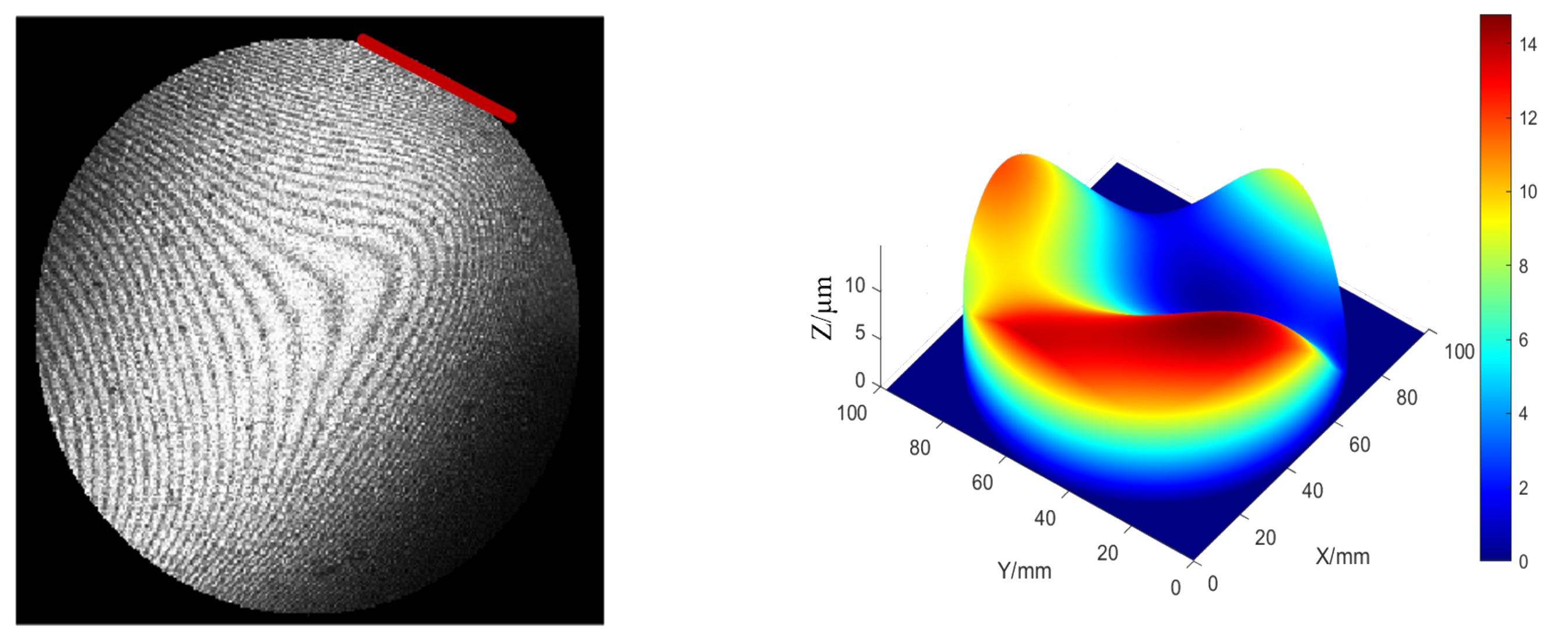
The comparative results for Samples 1 and 2, measured using both systems, are presented in Figure 5, Figure 6, Figure 7 and Figure 8. The left side of each figure shows the raw interferograms captured by the camera, with the red line in the diagram representing the wafer’s orientation flat. Slight edge shadowing, caused by the oblique camera view, is observable but does not compromise the accuracy of the reconstructed surface topography. These artifacts were effectively suppressed through subsequent image processing procedures, including binarization and thresholding.
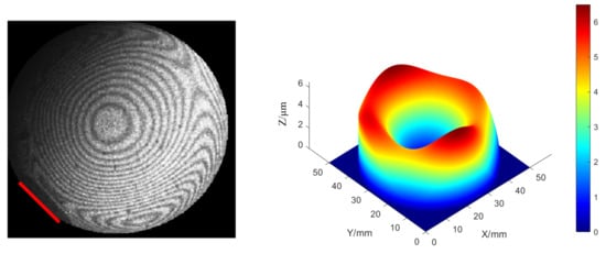
Figure 5.
Sample 1 (2-inch wafer) measured by the proposed system.
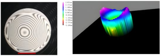
Figure 6.
Sample 1 (2-inch wafer) measured by the Tropel Flatmaster MSP 150.
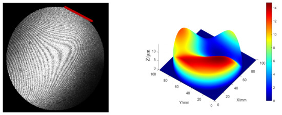
Figure 7.
Sample 2 (4-inch wafer) measured by the proposed system.
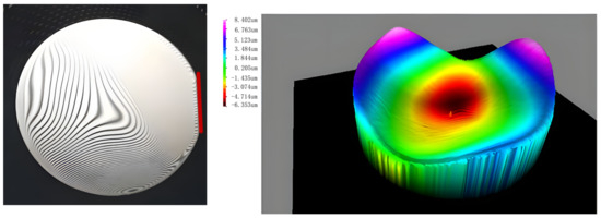
Figure 8.
Sample 2 (4-inch wafer) measured by the Tropel Flatmaster MSP 150.
During testing, the wafers were aligned using their orientation flats and placed at consistent measurement positions. Each sample was measured ten times under identical conditions. The surface height variation—defined as the height difference between the peak of the reconstructed surface profile and the reference plane—was used as the evaluation metric to quantify consistency between the two systems. For Sample 1, the proposed method yielded a mean height variation of , while the reference instrument reported . For Sample 2, the measured values were and , respectively.
These experimental results demonstrate that the interference fringe images acquired by the proposed system maintained stable quality, and the reconstructed surface topographies closely matched those obtained using the reference instrument. The proposed system exhibited excellent repeatability and measurement precision, confirming its feasibility and practical applicability for high-accuracy surface topography measurement of large-scale wafers.
Furthermore, the proposed measurement method and its corresponding image processing algorithms exhibit significant advantages in processing efficiency compared to the selected reference instrument. Taking Sample 1 as an example, the proposed system required an average of less than 1 minute per measurement cycle—from interferogram acquisition to surface topography reconstruction—whereas the reference device required more than 10 minutes for the same task. For Sample 2, the proposed method achieved an average processing time of under 2 minutes, in contrast to over 15 minutes for the reference instrument. These results highlight the system’s capability for rapid full-field surface characterization, significantly enhancing measurement throughput for large-scale wafers.
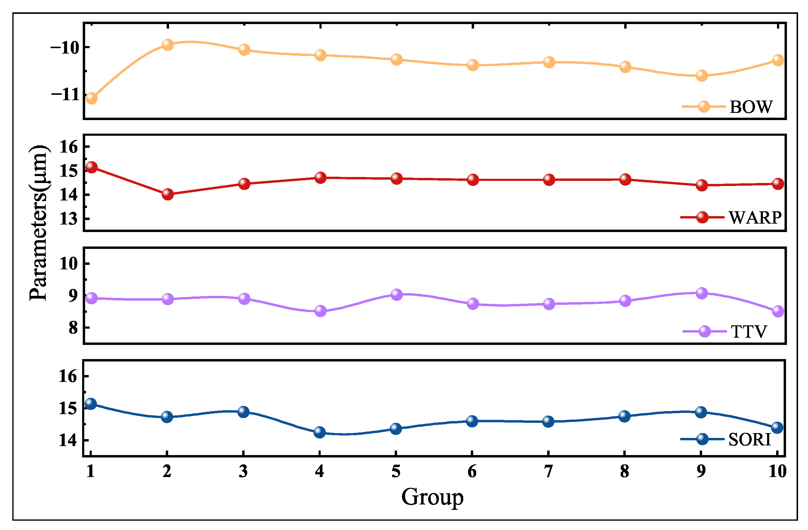
To further assess the completeness and accuracy of the measurement results, four standard surface topography parameters commonly used in silicon wafer quality evaluation were employed: BOW, WARP, TTV and SORI. These metrics offer quantitative descriptions of key geometric characteristics of the wafer surface. Figure 9 and Figure 10 presents the statistical results obtained from repeated measurements on both Samples 1 and 2 using the proposed system.
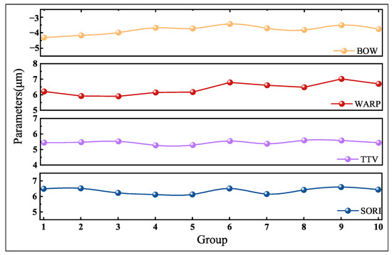
Figure 9.
Statistical results of BOW, WARP, TTV and SORI for Sample 1.
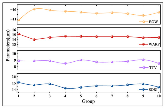
Figure 10.
Statistical results of BOW, WARP, TTV and SORI for Sample 2.
As shown in Figure 9 and Figure 10, for Sample 1, the measured average values of BOW, WARP, TTV and SORI were , , , and , respectively. The corresponding standard deviations ranged from to , indicating high measurement stability. For Sample 2, the corresponding average values were (BOW), (WARP), (TTV), and (SORI), exhibiting standard deviations between and , which confirms the system’s reliability for practical wafer quality assessment. Additionally, comparative evaluations between the proposed method and the reference instrument, as summarized in Table 1 and Table 2.

Table 1.
Comparison of measurement results between proposed system and reference instrument for Sample 1.

Table 2.
Comparison of measurement results between proposed system and reference instrument for Sample 2.
As shown by the comparative data in Table 1 and Table 2, the measurement results obtained from the proposed system are highly consistent with those of the reference instrument. For Sample 1, the absolute deviations of all four evaluation parameters were less than , with the maximum relative error not exceeding . For Sample 2, the absolute deviations of the corresponding parameters were all within , and the maximum relative error remained below . These results clearly demonstrate that the proposed thin-film interference-based surface topography measurement system achieves high measurement accuracy, along with excellent repeatability and system stability.
In summary, the experimental results confirm that the proposed system enables full-field rapid surface topography measurement for wafers within a 100 field of view, achieving a measurement accuracy on the order of 0.25 . The designed interferogram processing workflow and surface reconstruction algorithm effectively extract fringe structures and accurately reconstruct three-dimensional surface profiles. The system consistently meets the expected precision and error control requirements. Moreover, compared with conventional contact or scanning-based measurement techniques, the proposed method exhibits clear advantages in measurement efficiency. It provides a high-resolution, non-contact, and efficient solution for rapid wafer quality assessment during semiconductor manufacturing processes.
6. Conclusions
We have presented a non-contact, full-field wafer surface measurement system based on thin-film interference, designed for rapid and high-precision topography characterization. The optical configuration, integrating an off-axis parabolic mirror, enables single-exposure acquisition over a field of view. A fringe order determination method based on image-connected domains improves the robustness of fringe analysis in complex patterns. Together with tailored image processing and surface reconstruction algorithms, the system achieves a measurement accuracy better than and sub-micron vertical resolution, with results in close agreement with those from a commercial reference instrument. The approach combines simplicity, scalability, and cost-effectiveness, making it well suited for high-throughput wafer inspection in industrial settings. Future work will address extending the measurement capability to larger wafer sizes by employing larger optical components and implementing a stitching-based method to further enhance scalability.
Author Contributions
Conceptualization, R.Y. and H.L.; methodology, J.Z., H.Z. and Y.S.; software, J.Z., H.Z. and Y.S.; validation, R.Y., Y.S. and H.L.; formal analysis, R.Y. and H.L.; investigation, Y.S.; resources, R.Y.; data curation, J.Z., H.Z. and Y.S.; writing—original draft preparation, Y.S.; writing—review and editing, R.Y. and H.L.; visualization, H.L.; supervision, R.Y.; project administration, R.Y. and H.L.; funding acquisition, R.Y. All authors have read and agreed to the published version of the manuscript.
Funding
This research was funded by National Key Research and Development Program (grant number 2024YFF0726102); National Natural Science Foundation of China (grant number 51605171).
Institutional Review Board Statement
Not applicable.
Informed Consent Statement
Not applicable.
Data Availability Statement
Data is contained within the article.
Conflicts of Interest
The authors declare no conflicts of interest.
References
- Miao, F.; Ahn, S.; Kim, Y. Precise measurement of the surface shape of silicon wafer by using a new phase-shifting algorithm and wavelength-tuning interferometer. Appl. Sci. 2020, 10, 3250. [Google Scholar] [CrossRef]
- Wu, D.; Fang, F. Development of surface reconstruction algorithms for optical interferometric measurement. Front. Mech. Eng. 2021, 16, 1–31. [Google Scholar] [CrossRef]
- Wang, Y.; Xie, F.; Ma, S.; Dong, L. Review of surface profile measurement techniques based on optical interferometry. Opt. Lasers Eng. 2017, 93, 164–170. [Google Scholar] [CrossRef]
- Zeng, Y.; Zhang, J.; Zhou, H.; Guo, H. A new processing technique for fabrication of ultra-thin wafer. Int. J. Adv. Manuf. Technol. 2019, 100, 1287–1298. [Google Scholar] [CrossRef]
- Lee, H.; Sung, J.; Park, S.; Shin, J.; Kim, H.; Kim, W.; Lee, M. Lens-free reflective topography for high-resolution wafer inspection. Sci. Rep. 2024, 14, 10519. [Google Scholar] [CrossRef]
- Marks, M.R.; Hassan, Z.; Cheong, K.Y. Ultrathin Wafer Pre-Assembly and Assembly Process Technologies: A Review. Crit. Rev. Solid State Mater. Sci. 2015, 40, 251–290. [Google Scholar] [CrossRef]
- Jäger, G.; Hausotte, T.; Manske, E.; Büchner, H.J.; Mastylo, R.; Dorozhovets, N.; Hofmann, N. Nanomeasuring and nanopositioning engineering. Measurement 2010, 43, 1099–1105. [Google Scholar] [CrossRef]
- Yang, C.; Dang, C.Q.; Zhu, W.L.; Ju, B.F. High-speed atomic force microscopy in ultra-precision surface machining and measurement: Challenges, solutions and opportunities. Surf. Sci. Technol. 2023, 1, 7. [Google Scholar] [CrossRef]
- Chein, W.H.; Pandey, G.; Das, S.; Chen, L.C. Advancements in metrology for advanced semiconductor packaging. In Proceedings of the Optics and Photonics for Advanced Dimensional Metrology III; De Groot, P.J., Guzman, F., Picart, P., Eds.; International Society for Optics and Photonics: Strasbourg, France, 2024; Volume 12997, p. 129970R. [Google Scholar]
- Jordan, H.J.; Wegner, M.; Tiziani, H. Highly accurate non-contact characterization of engineering surfaces using confocal microscopy. Meas. Sci. Technol. 1998, 9, 1142. [Google Scholar] [CrossRef]
- Fratz, M.; Seyler, T.; Bertz, A.; Carl, D. Digital holography in production: An overview. Light Adv. Manuf. 2021, 2, 283–295. [Google Scholar] [CrossRef]
- Zhao, X.; Yu, T.; Liang, D.; He, Z. A review on 3D measurement of highly reflective objects using structured light projection. Int. J. Adv. Manuf. Technol. 2024, 132, 4205–4222. [Google Scholar] [CrossRef]
- Yang, S.; Zhang, G. A review of interferometry for geometric measurement. Meas. Sci. Technol. 2018, 29, 102001. [Google Scholar] [CrossRef]
- Huang, G.; Cui, C.; Lei, X.; Li, Q.; Yan, S.; Li, X.; Wang, G. A Review of Optical Interferometry for High-Precision Length Measurement. Micromachines 2024, 16, 6. [Google Scholar] [CrossRef] [PubMed]
- Yang, Y.; Han, S.; Zhang, L.h.; Shen, Y.h.; Xu, C.f. Surface profile measurement and parameter analysis of silicon wafers in the upright state. Appl. Opt. 2024, 63, 2587–2593. [Google Scholar] [CrossRef] [PubMed]
- Michalska, A.; McKendrick, D.; Weston, N.; Shephard, J.d. Incoherent light interferometer for single-shot, dual wavelength, areal topography measurements of a reflective surface. Opt. Express 2025, 33, 1760–1771. [Google Scholar] [CrossRef] [PubMed]
- Zhang, W.; Zhang, H.; Wang, B.; Meng, K.; Lou, P. Efficient white light interferometry for wafer-scale high aspect ratio structures. Measurement 2025, 255, 117988. [Google Scholar] [CrossRef]
- Cheng, F.; Zou, J.; Su, H.; Wang, Y.; Yu, Q. A differential measurement system for surface topography based on a modular design. Appl. Sci. 2020, 10, 1536. [Google Scholar] [CrossRef]
- Su, H.; Ye, R.; Cheng, F.; Cui, C.; Yu, Q. A Straightness Error Compensation System for Topography Measurement Based on Thin Film Interferometry. Photonics 2021, 8, 149. [Google Scholar] [CrossRef]
- Niblack, W. An Introduction to Digital Image Processing; Strandberg Publishing Company: Birkeroed, Denmark, 1985. [Google Scholar]
- Zhang, T.Y.; Suen, C.Y. A fast parallel algorithm for thinning digital patterns. Commun. ACM 1984, 27, 236–239. [Google Scholar] [CrossRef]
- Area, I.; Dimitrov, D.K.; Godoy, E. Recursive computation of generalised Zernike polynomials. J. Comput. Appl. Math. 2017, 312, 58–64. [Google Scholar] [CrossRef]
Disclaimer/Publisher’s Note: The statements, opinions and data contained in all publications are solely those of the individual author(s) and contributor(s) and not of MDPI and/or the editor(s). MDPI and/or the editor(s) disclaim responsibility for any injury to people or property resulting from any ideas, methods, instructions or products referred to in the content. |
© 2025 by the authors. Licensee MDPI, Basel, Switzerland. This article is an open access article distributed under the terms and conditions of the Creative Commons Attribution (CC BY) license (https://creativecommons.org/licenses/by/4.0/).

