1. Introduction
Plasmonics is perhaps the most flourishing research area of optics in the recent decades as it offers unprecedented control over light with nanometer precision in very small volumes. A plethora of applications ranging from photovoltaics to optical integrated circuitry hold promise for revolutionizing the way technology deals with light. Major contribution to the plasmonics discipline has been provided by the nanotechnology advent which has made plausible the realization of miniaturized metallic structures and devices able to interact with light via plasmon excitations. To this end, top-down technologies and lithographic techniques have been employed for the realization of periodic plasmonic nanostructures (plasmonic lattices) without geometrical and structural constrains. Another approach are the so-called bottom-up approaches based on self-assembly technology allowing for the realization of periodic plasmonic nanostructures with the promise of lower cost, high throughput, and small sensitivity to damage or fabrication errors [
1]. The only restriction in the bottom-up techniques had been the shape of repeating units (nanoparticles) which is mainly spherical or nearly spherical (spheroids, ellipsoids,
etc). Recently, new chemical approaches have made plausible the fabrication of particles with sharp edges such as nanocubes [
2,
3,
4,
5,
6,
7]. The advantage of realizing particles with sharp edges is that when they are brought very close together, (e.g., in a dimer of nanocubes) or in proximity to flat surfaces, space gaps of a few nm may be feasible. Such nanosized gaps (nanogaps) have the functionality to localize light within their volume boosting the local electric field by several orders of magnitude.
Another important functionality which has been recently introduced for metallic nanocubes is that of tunable enhanced absorption [
3]. Namely, a single nanocube in close proximity to a metallic film,
i.e., a so-called film-coupled nanocube, can exhibit a much stronger absorption spectrum from an isolated nanocube due to the excitation of effective magnetic-surface currents in the gap between the nanocube and the film. The smaller the gap, the higher are these magnetic currents due to their proportionality to the local electric field. These effective magnetic currents generate secondary EM waves (reflected waves) which can exactly cancel the secondary EM waves (also reflected waves) emitted by the electric-surface currents resulting in suppressed reflection [
3]. And, as metals are lossy in the optical regime, an EM wave which is not efficiently reflected at the surface, it is eventually absorbed by the metal. The EM response of a metallic nanocube coupled to a metallic film resembles the response of grounded patch antenna in the microwave regime,
i.e., a metallic patch above a conducting plane.
So far, the theoretical study of such systems has been focused on the EM response of a single nanocube coupled to a metallic substrate [
3,
4,
5,
6,
7]. This is a fair treatment when the metallic film supports dilute arrays of metallic nanotubes. However, when nanocubes approach each other, multiple scattering of light among the nanocubes starts affecting the overall response rendering the single-nanocube approach inadequate. Furthermore, a periodic array of nanocubes may possess additional functionalities if viewed as a periodic metasurface [
8]. In the present work, we study the optical response of periodic arrays of nanocubes positioned over a metallic film wherein the gap between the periodic array and the substrate is filled by a dielectric material. In particular, we study the conditions under which light absorbance is enhanced and tuned by varying the geometrical parameters of the system and the angle of incidence.
2. Calculation Method
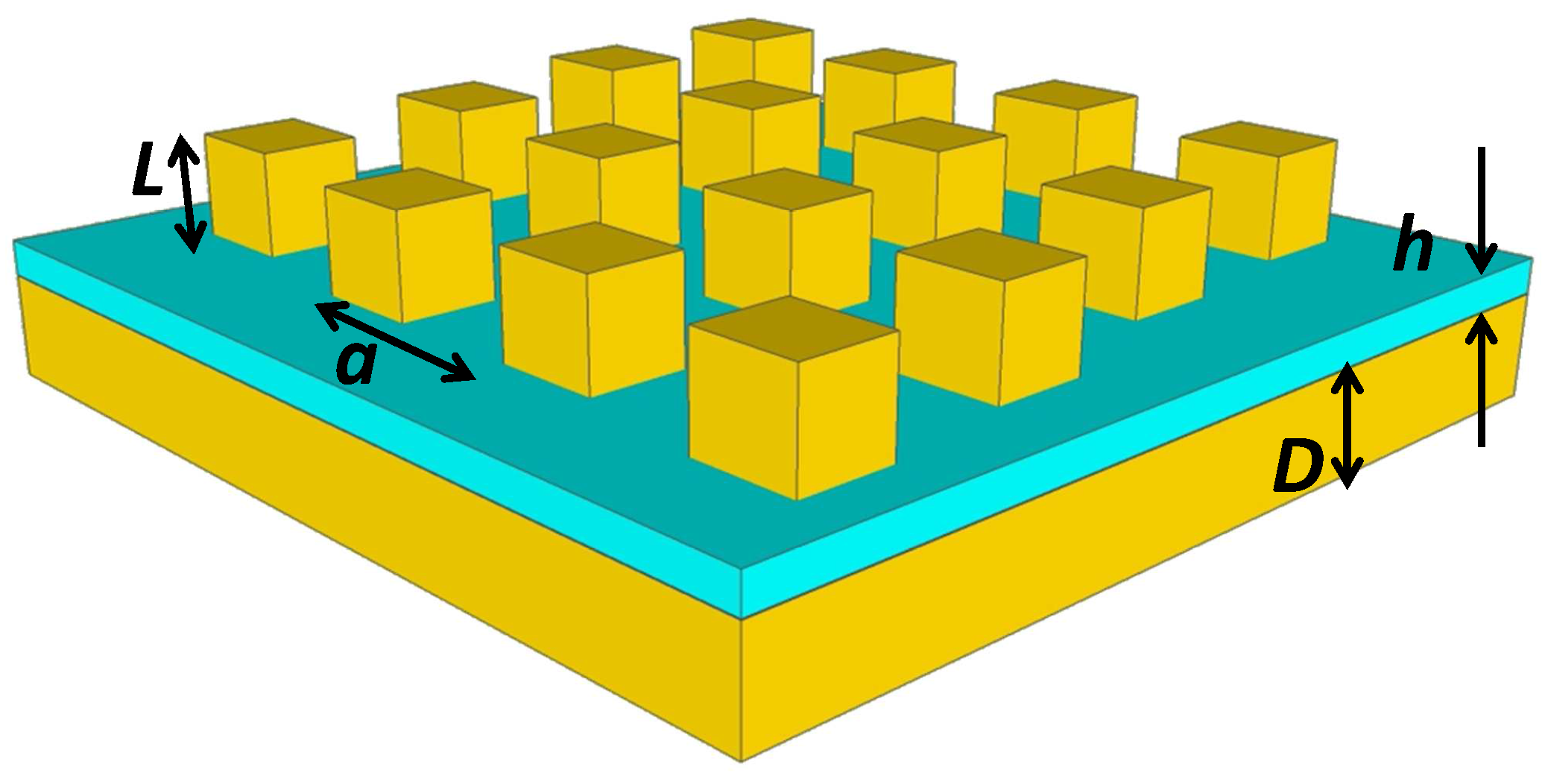
The system under study is depicted in
Figure 1: periodic array of cubes placed atop a thin film and a thicker substrate. Similar systems,
i.e., periodic arrays of nanoparticles on top of metallic films/ substrates have been the focus of intensive studies [
9,
10,
11,
12]. Such systems,
i.e., periodic arrays of spherical scatterers atop films [
13,
14] are easily dealt with the layer-multiple scattering method. Namely, to model such a structure we employ a hybrid layer-multiple-scattering (hLMS) method based on a discrete-dipole approximation (DDA)/T-matrix point matching method [
15]. The hLMS method is an extension of the traditional LMS which is used for two- (2D) and three- (3D) dimensional arrays of spheres [
16,
17,
18] and axisymmetric scatterers [
19]. Namely, the hLMS method treats scatterers of arbitrary shape, anisotropy and inhomogeneity by calculating the scattering T-matrix of a single scatterer by a DDA/T-matrix point-matching technique [
15]. Having calculated the T-matrix, one proceeds similarly to the standard LMS method. Namely, the EM field within a given 2D lattice (plane) of spheres is obtained via the multiple-scattering technique. In between a pair of two consecutive planes of spheres, the EM field is written in a plane wave basis where the multiple-scattering between the planes is fully taken into account. A slab of macroscopic thickness,
i.e., containing up to several hundreds of planes of general scatterers, can be easily built up via a doubling-layer process [
16,
17,
18]. By imposing boundary conditions along the growth direction of the crystal slab, one can also calculate the complex frequency band structure [
16,
17,
18].
Figure 1.
A square array of metallic nanocubes separated with a thin dielectric film from a metallic substrate. The lattice constant of the square array is denoted by a, the edge of the nanocubes by L, the thickness of the dielectric film by h and the thickness of the metallic substrate by D.
Figure 1.
A square array of metallic nanocubes separated with a thin dielectric film from a metallic substrate. The lattice constant of the square array is denoted by a, the edge of the nanocubes by L, the thickness of the dielectric film by h and the thickness of the metallic substrate by D.
3. Results and Discussion
The plasmonic design under study are depicted in
Figure 1. The geometrical of as well as the material parameters are taken from Ref. [
3]. The dielectric function of gold and silver have been taken from experiment [
20]. Note that the experimental data of Ref. [
3] are collected from dilute, random arrays of nanocubes, and, as such, they were associated with the optical properties of a single film-coupled nanocube. Therefore, direct comparison of our numerical results that follow with experiment is not possible.
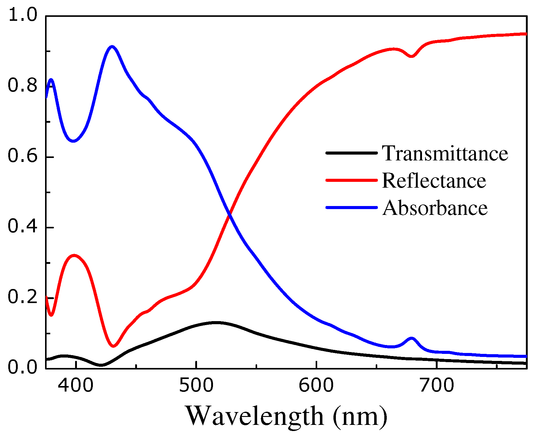
In
Figure 2 we show the transmittance, reflectance and absorbance spectra for light incident normally on a square array (of lattice constant
nm) of silver nanocubes with edge
nm, separated by a 8 nm polyelectrolyte (
) spacer from a 50 nm thick gold substrate. Evidently, the system is very opaque as the corresponding transmittance does not exceed 10% in the depicted spectral region. There is a cross-over region at about 530 nm above which light absorption decreases and strong reflectance sets out. The high-frequency peaks at
nm and 400 nm originate from the surface plasmon (SP) modes of the single nanocube which interact with the corresponding modes of their neighbouring nanocubes resulting in a SP absorption band [
21]. On the other hand, the small absorption peak at about 680 nm stems from a waveguide cavity mode [
4] wherein the cavity is formed by the space between the nanocube and the underlying metallic substrate. These cavity modes are leaky modes and can, therefore, couple to externally incident light giving rise to the observed peak in the absorbance and reflectance spectra of
Figure 2.
Figure 2.
Transmittance, reflectance and absorbance of light incident normally on a square array (of lattice constant
nm) of silver nanocubes with edge
nm, separated by a 8 nm polyelectrolyte (
) spacer from a 50 nm thick gold substrate (see
Figure 1).
Figure 2.
Transmittance, reflectance and absorbance of light incident normally on a square array (of lattice constant
nm) of silver nanocubes with edge
nm, separated by a 8 nm polyelectrolyte (
) spacer from a 50 nm thick gold substrate (see
Figure 1).
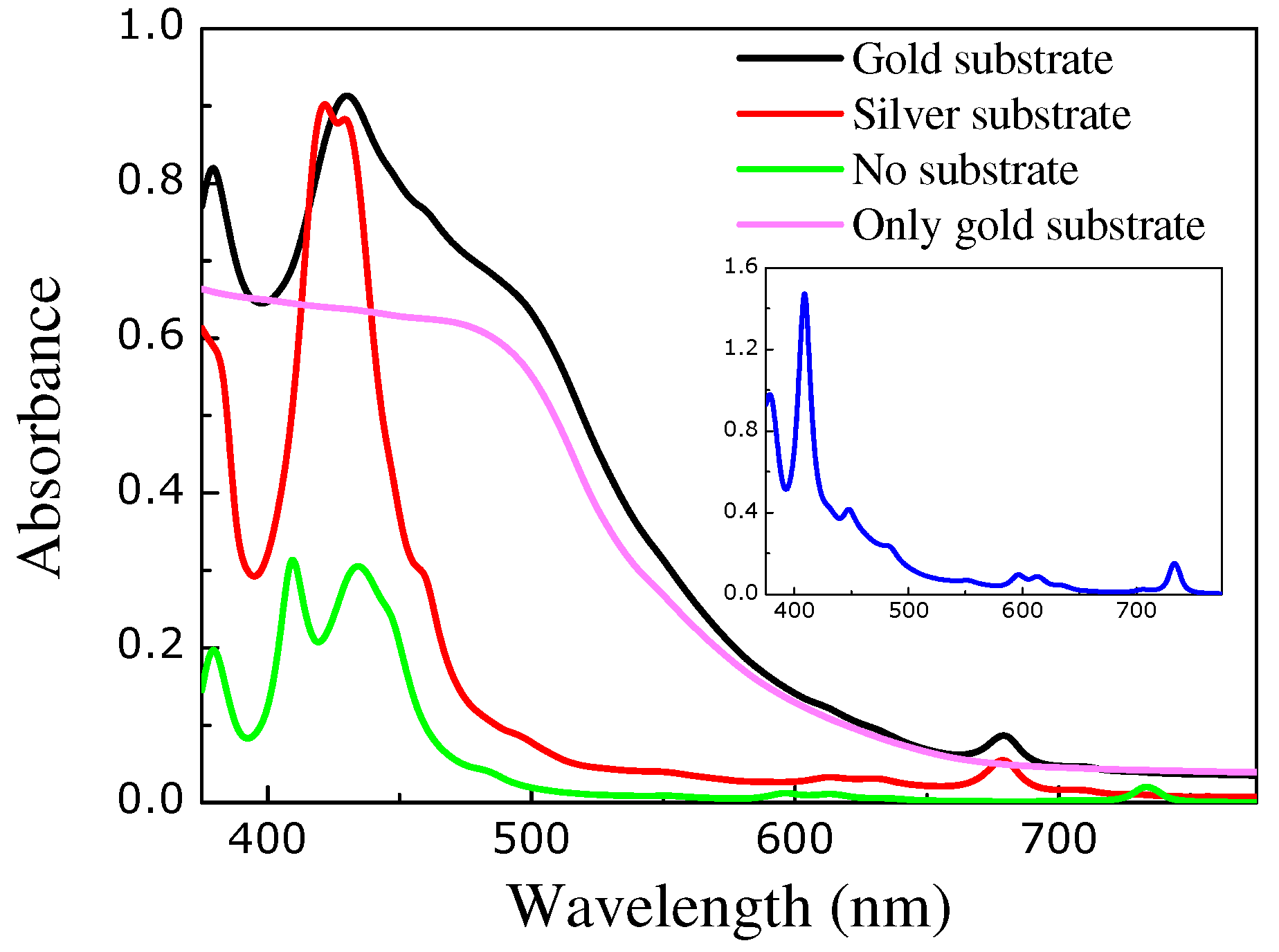
Figure 3.
Absorbance of normally incident light on the array of nanocubes described in
Figure 2 with or without a metallic substrate. The substrate is 50 nm thick and is either gold or silver. The inset shows the absorption cross section for light incident normally on a
single nanocube.
Figure 3.
Absorbance of normally incident light on the array of nanocubes described in
Figure 2 with or without a metallic substrate. The substrate is 50 nm thick and is either gold or silver. The inset shows the absorption cross section for light incident normally on a
single nanocube.
The fact that the short-wavelength peaks of the absorbance spectrum of
Figure 2 are particle-like SP nature while the smaller low-frequency (long wavelength) peak are of cavity-like SP origin, is clearly understood from
Figure 3. Namely,
Figure 3 shows the absorbance spectra for light incident normally on the array of nanocubes of
Figure 2 for gold/ silver substrate or in the absence of a metallic substrate. Evidently, the long-wavelength absorbance peak at 680 nm is not present for a square lattice of nanocubes alone (without the substrate) suggesting the cavity-like nature of the corresponding mode. The short-wavelength peaks exist in all cases (single nanocube, arrays of nanocubes with or without the metallic substrate) implying that they originate from the interaction of particle-like modes of the single nanocube. However, the amount of absorption corresponding to the arrays with the metallic substrate (gold or silver) is much higher than for the array of nanocubes alone (without the substrate). This is the effect of magnetic-current generation in the space between a cube and the substrate which matches the impedance of the structure with that of vacuum leading to enhanced light transmission and subsequently enhanced absorption [
3]. For example, the presence of gold substrate increases the height absorption peak of the single nanocube array at 377 nm by more than 4 times. Both gold and silver substrates increase the overall absorption of the nanocube array (up to 500 nm) but the gold substrate provides a much broader absorbance spectrum than the silver one. Lastly, there is an absorption peak at about 735 nm in the cross section of a single silver nanocube (inset of
Figure 3) as well as in the absorbance spectrum of the array without the substrate suggesting that the corresponding mode is highly localized at the nanocube. However, this peak vanishes in the presence of the substrate as it submerges within the background absorption of the metallic substrate.
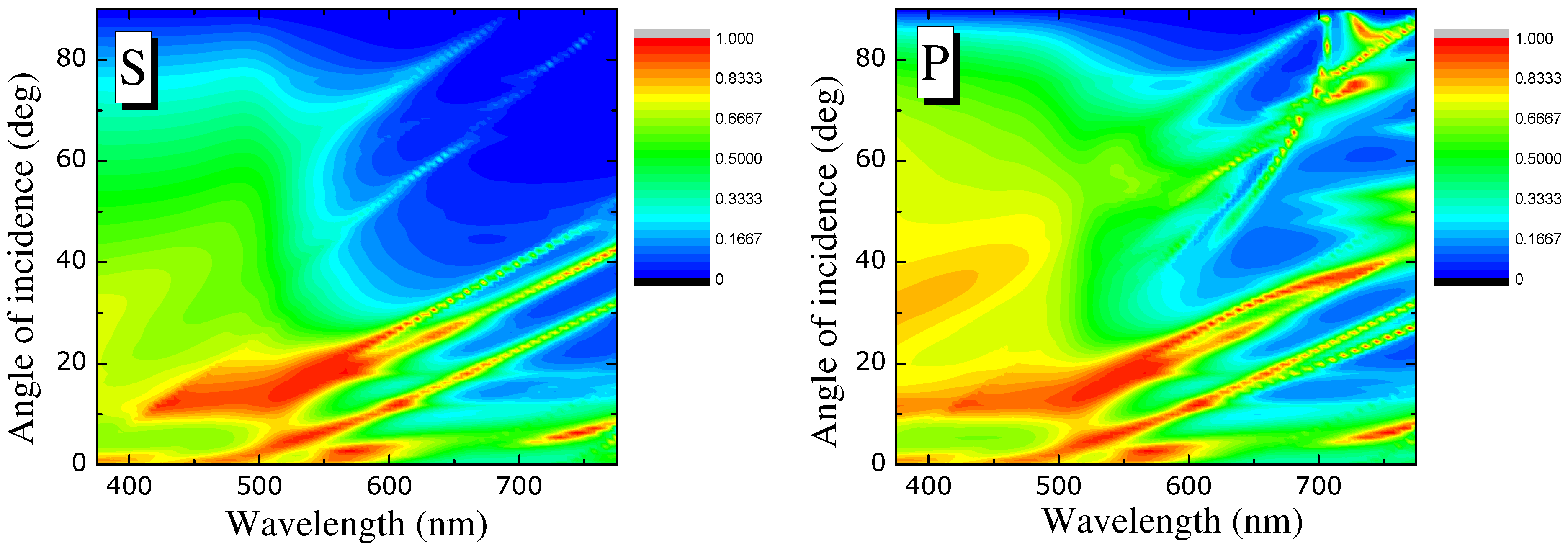
Figure 4.
Absorbance vs angle of incident for
s- (left panel) and
p-polarized (right panel) light incident on the square array of nanocubes of
Figure 2 atop an 8 nm polyelectrolyte film and 50 nm gold substrate.
Figure 4.
Absorbance vs angle of incident for
s- (left panel) and
p-polarized (right panel) light incident on the square array of nanocubes of
Figure 2 atop an 8 nm polyelectrolyte film and 50 nm gold substrate.
The spectra studied so far are for normally incident light. In
Figure 4 and
Figure 5 we explore the dependence of the absorbance spectra on the angle of incidence and state of polarization of the incident light. Evidently, for both types of substrate materials, the absorbance spectra do not differ much on the polarization of incident light apart from some additional peak structure which emerges for high angles and
p-polarized incident light. This in accordance with the increased scattering spectrum for a single nanocube on a substrate for p-polarized light evidenced in [
4]. The peak at 680 nm observed in
Figure 3 corresponding to a cavity-like mode wherein light is confined between the nanocube and the metallic substrate, shows some considerable angular dispersion (see
Figure 4 and
Figure 5) due to the interaction of these cavity-like modes with their counterparts in neighboring nanocubes. We also observe an almost linear dependence of the position of several absorption peaks on the angle of incidence, for both polarizations and
Figure 4 and
Figure 5. These peaks stem from the slab modes of the single metallic substrate. Namely, for a single metallic substrate, these slab modes decay exponentially away from the surfaces of the substrate and, hence, do not couple with incident light. However, in the presence of the periodic array of nanocubes, these modes become leaky by the underlying periodicity (Umklapp process) of the nanocube array manifesting themselves as absorbance peaks in the corresponding spectrum. The above trends are observed for both types of substrate materials although for the silver substrate there exists an additional peak at about 470 nm and for angles of incidence around
.
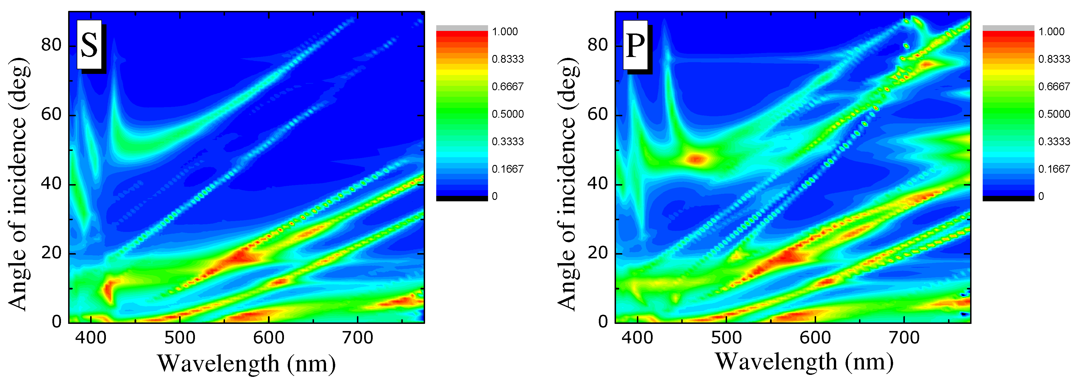
Figure 5.
The same as
Figure 4, but for a silver substrate.
Figure 5.
The same as
Figure 4, but for a silver substrate.
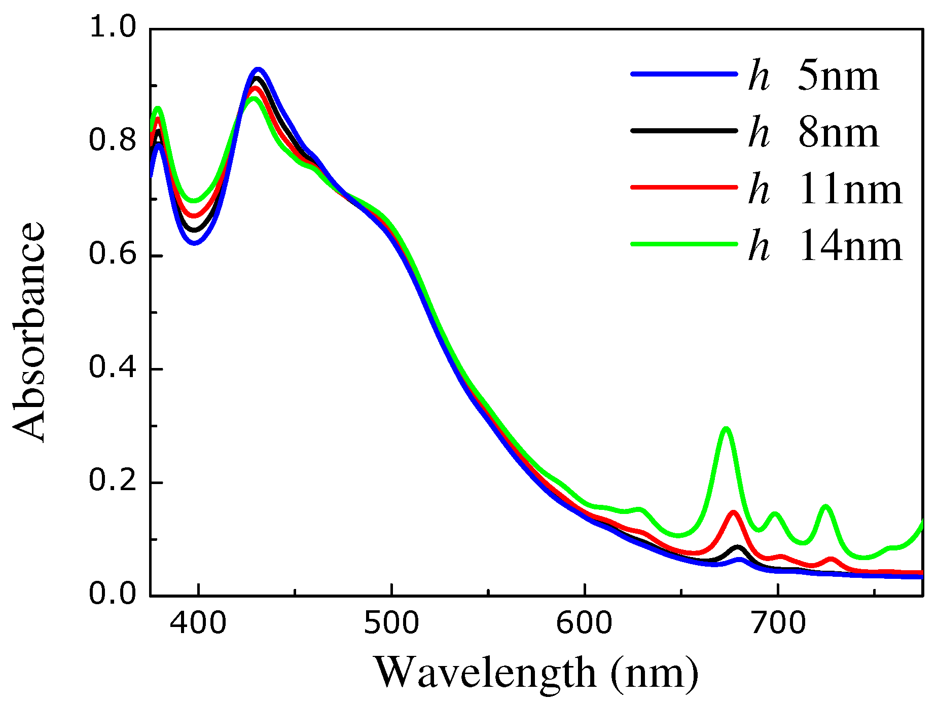
In
Figure 6 we study the role of the dielectric spacer in the absorbance spectra. The short-wavelength peaks which are present irrespective of the presence of a metallic substrate are, as expected, less influenced by the thickness of the dielectric spacer than the cavity-like peaks at longer wavelengths. Moreover, the height of the cavity-like peaks increases with increasing spacer thickness due to more efficient coupling of incoming radiation with the cavity modes.
Figure 6.
Absorbance of normally incident light on the array of nanocubes described in
Figure 2 separated from a 50 nm gold substrate by a polyelectrolyte film for different thicknesses,
i.e.,
nm.
Figure 6.
Absorbance of normally incident light on the array of nanocubes described in
Figure 2 separated from a 50 nm gold substrate by a polyelectrolyte film for different thicknesses,
i.e.,
nm.
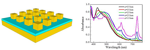
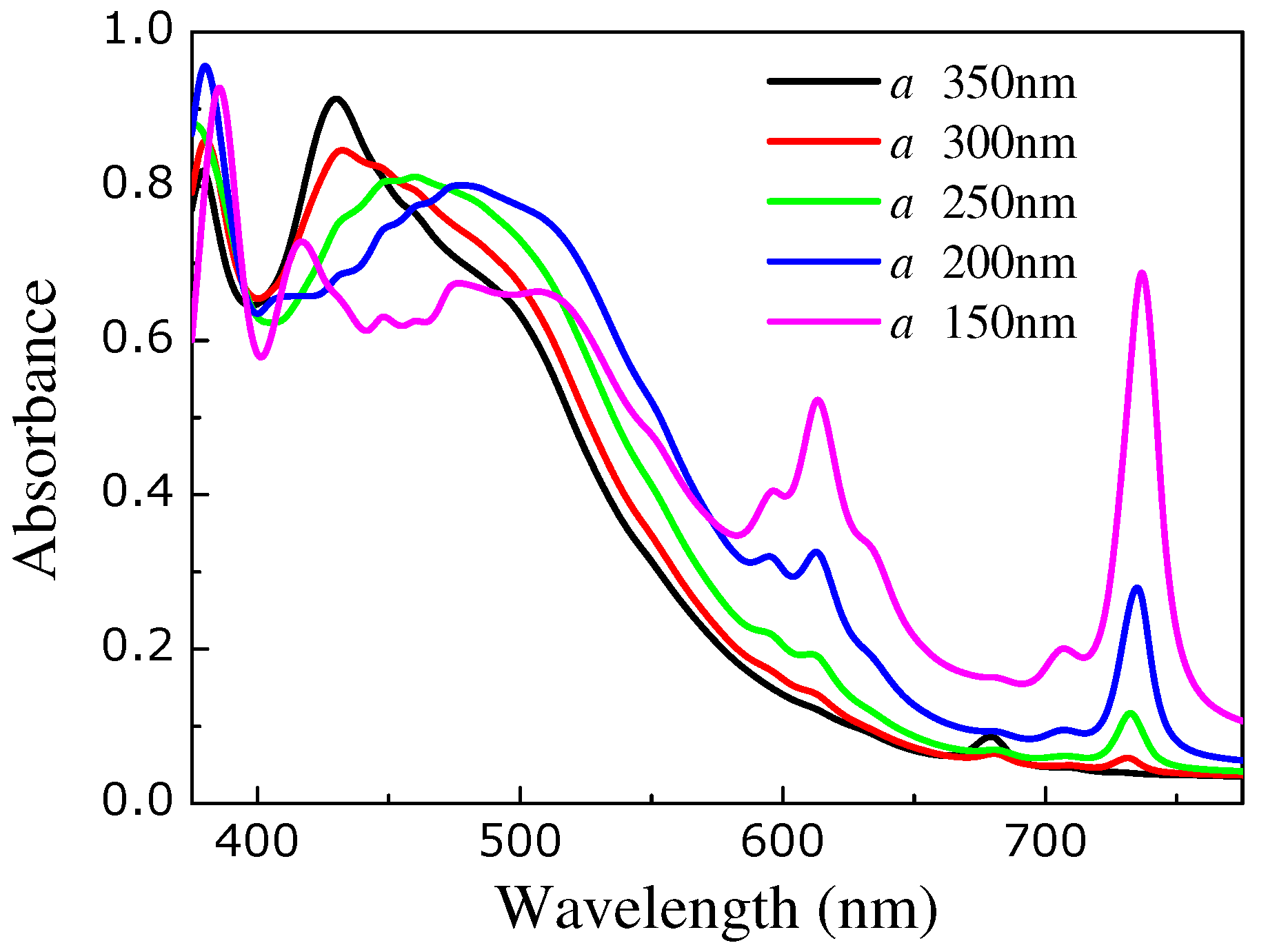
Next, in
Figure 7 we show the absorbance spectra for arrays of 70 nm nanocubes on gold substrate, for different lattice constants. We observe that as the lattice constant decreases and the interaction of the SP modes of neighbouring nanocubes increases, the absorbance peaks shift to longer wavelengths (red shift) and become much wider, as expected. However, additional peak structure emerges with decreasing lattice constant attributed primarily to the higher-multipole SP excitations at the nanocubes [
21]. The long-wavelength (cavity-like) SP peak above 700 nm increases dramatically with the reduction of the lattice constant as the cavity modes underneath each nanocube interact more strongly with each other. Most notably, th peak structure slightly above 600 nm is drastically enhanced by the interaction between the nanocubes leading to prominent absorption peak not evidenced for large lattice constants.
Figure 7.
Absorbance of light incident normally on a square array of silver nanocubes with edge
nm, separated by a 8 nm polyelectrolyte (
) spacer from a 50 nm thick gold substrate (see
Figure 1), for different lattice constants,
i.e.,
nm.
Figure 7.
Absorbance of light incident normally on a square array of silver nanocubes with edge
nm, separated by a 8 nm polyelectrolyte (
) spacer from a 50 nm thick gold substrate (see
Figure 1), for different lattice constants,
i.e.,
nm.
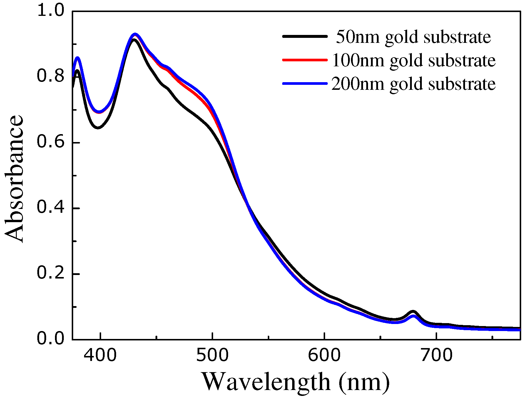
Finally, in
Figure 8 we vary the thickness of the gold substrate. Evidently, as we increase the thickness of the substrate we do not observe a dramatic increase in the total absorbance; actually, there is practically no difference between the absorbance spectra for
nm and 200 nm as absorbance saturates above a certain value of the thickness.
Figure 8.
Absorbance of light incident normally on the square array of silver nanocubes
Figure 3 with edge
nm, separated by a 8 nm polyelectrolyte (
) spacer from a gold substrate (see
Figure 1), for different substrate thicknesses,
nm.
Figure 8.
Absorbance of light incident normally on the square array of silver nanocubes
Figure 3 with edge
nm, separated by a 8 nm polyelectrolyte (
) spacer from a gold substrate (see
Figure 1), for different substrate thicknesses,
nm.


