Abstract
For the first time, we are able to generate over 1000 diffraction spots from a graded photonic super-crystal with a unit super-cell size of 12a × 12a where a is the lattice constant and hole radii are gradually changed in dual directions. The diffraction pattern from the graded photonic super-crystal reveals unique diffraction properties. The first order diffractions of (±1,0) or (0,±1) disappear. Fractional diffraction orders are observed in the diffraction pattern inside a square with vertices of (1,1), (1,−1), (−1,−1) and (−1,−1). The fractional diffraction can be understood from lattices with a period of a. However, a dual-lattice model is considered in order to explain higher-order diffractions. E-field intensity simulations show a coupling and re-distribution among fractional orders of Bloch waves. There are a total of 12 × 12 spots in E-field intensity in the unit supercell corresponding to 12 × 12 fractional diffraction orders in the diffraction pattern and 12 × 12 fractional orders of momentum in the first Brillouin zone in k-space.
1. Introduction
Beam diffraction from crystals has been used to study crystals or quasi-crystals and obtain the information of lattice period and symmetry [1,2]. On the other hand, meta-surfaces and photonic crystals are designed to manipulate, steer or diffract light beams [3,4,5]. Meta-grating, one type of meta-surfaces, has been demonstrated to deflect light to a 75 degree angle or steer the light beam to desired diffraction orders [5]. Typical two-dimensional (2D) photonic crystals are periodically arranged rods in air or holes in the substrate with uniform sizes of rods or holes and the same filling fraction [6]. When the Bragg diffraction from different wave-vector directions from the photonic crystal occurs at the same wavelength, a photonic band gap forms in the crystal [7]. Graded photonic crystals with gradual size changes of rods (holes) or gradual period changes of lattices has been developed and used to bend, split or nano-focus the light beam [8,9,10,11].
Very recently, graded photonic super-crystals (GPSCs) have been fabricated through the interference lithography by two sets of multiple beams arranged in a cone geometry [12,13,14]. The GPSC has two sets of lattices: the rod size (or hole size) increases gradually along one direction in one set of lattices while the other set decreases their sizes gradually. GPSC has dual period and even dual symmetry: The square lattices in GPSC have a small period while graded regions have their own symmetry and period [12,13,14]. GPSCs can be used to enhance the broadband light trapping in an Si solar cell, broadband light extraction from organic light emitting diode, and to form a resonance cavity at the boundary of graded and less-graded regions [15,16,17]. By incorporating disorders in the location and radii of the holes in the 2D photonic crystal, topological properties appear in the photonic crystal [18,19].
Light-emitting diodes (LEDs) and fluorescent molecules have excellent color features, long life time and provide a less-expensive solution to lighting [20,21,22]. The lighting system can be composed of one LED shinning on a GPSC that can have many diffraction spots and fluorescent molecules encapsulated in glass whose fluorescence is excited by the diffracted LED sources.
In this paper, we observed unique diffraction properties in a fabricated GPSC where the radii of holes are gradually changed in dual directions. Over 1000 diffraction spots were observed. The diffraction pattern was explained by the fractional orders of momentum & dual-lattice model and by electromagnetic simulations.
2. Fabrication and Simulation Methods
The GPSC pattern was designed using an E-beam exposure control program. The hole size in GPSC was obtained from the interference pattern as described in the next section. Polymethylmethacrylate (PMMA) A2 was spin-coated on an Si substrate at a speed of 3500 RPM for 45 s using Laurell WS-650 tabletop spin coater. Thus, a thickness of 66 nm was expected. The PMMA thin film was post-baked for 90 s at 180 °C. JEOL JSM-7001F SEM and EBL pattern generator were used for E-beam lithography. The exposed PMMA film was developed in a solution of isopropanol and distilled water in the ratio 3:1 for 10 s. Al film with a thickness of 75 nm was deposited using KJLC NANO-36 thin film deposition system.
The interference intensity I(r) as a function of location r was calculated. The following step function was used to generate Al GPSC: permittivity of Al, which was sourced from a reference [23], was applied when I(r) was less than a threshold intensity Ith, and air when I(r) > Ith. A finite-difference time-domain (FDTD) open-source software tool MIT MEEP program [24] was used for the simulation of the reflection from Al GPSC and of E-field. The simulations were performed through cloud-based parallel computations at Amazon Web Service using 36-core virtual machines at the Simpetus Electromagnetic Simulation Platform. For the reflection, a broadband plane wave was used. For the E-field, we used 532 nm wavelength.
3. Results
Multiple-beam laser interference lithography has been used for the holographic fabrication of GPSCs [12,13,14]. Here the interference pattern is used to design the pattern for the electron-beam lithography and also as an input for the FDTD simulation of E-field intensity and reflection from the GPSC. Eight beams of coherent light are used to form the interference pattern and these eight beams can be generated through a spatial light modulator [12]. Four of them (red lines in Figure 1a) are arranged in a cone geometry with a cone angle of 2θ1 and others (blue lines Figure 1a) with a cone angle of 2θ2. The interference intensity as a function of location r can be calculated from Equation (1):
where E and e are the electric field strength and polarization, respectively, k is the wave vector, and δ is the initial phase. The eight beams have their wave vectors of: {k1 … k8} = {k(sin(θ)cos(45 + n × 90)o, sin(θ)sin(45 + n × 90)°, cos(θ)), n = 0,1,2,3, where θ = θ1 for beams represented by red line and θ = θ2 for those by blue lines in Figure 1a. When θ1 = 22.1 degrees and wavelength = 532 nm, the small period ΛS equals approximately 2π/(2ksin(θ1) × sin45) = 1000 nm. The big period can be approximately estimated by ΛL = 2π/(ksinθ2) = 12,100 nm when θ2 = 1.79 degrees in Figure 1a.
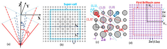
Figure 1.
(a) Schematic of eight beams arranged in a cone geometry. (b) Designed patterns for E-beam lithography for the generation of GPSC with a unit cell size of 12a × 12a. (c) Enlarged view of the pattern in (b) with labels of lattice planes. (d) Fractional orders of momentum increasing by 2π/(12a) in the reciprocal space.
After the iso-intensity surface of eight-beam interference pattern is generated using Matlab program, radii of holes in the unit cell of 12a × 12a are read by the program. These radii are manually input into the E-beam exposure control program. The program allows an assignment of hole radii in a unit cell, indicated by the dash square in Figure 2b. For example, along the dash arrow L3, radii of holes are 255.8, 280, 240.7, 290, 227.3, 320, 220, 320, 227.3, 290, 240.7, and 280 nm, respectively. The dash arrow L6 has holes with radii of 255.8, 230.3, 370.2, 223, 420.7, 223.7, 450.7, 223.7, 420.7, 223, 370.2, and 230.3 nm, respectively.
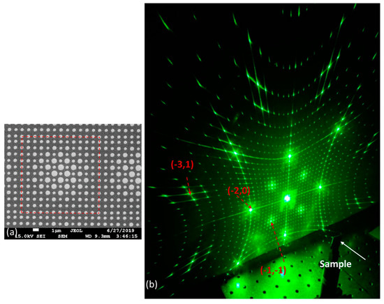
Figure 2.
(a) SEM of fabricated GPSC in PMMA. (b) Diffraction pattern from the GPSC using 532 nm laser.
In the simulation, we used a symmetric unit cell as indicated by the solid square. The lattice constant a = 1000 nm and unit super-cell size is 12a × 12a. Figure 1c shows an enlarged view of the pattern in (b) for the central area of the unit super-cell. The lattices can be classified as two types with a small hole or big hole: The radii of small holes are increasing along the blue arrow while the radii of big holes are decreasing along the red arrow. Miller indices (1,0), (1,1) and (1,3) are labelled for crystal planes indicated by dash purple, blue and red lines, respectively. The radius difference relative to holes at the edge of the super-cell is indicated by ∆Ri and ∆Rj in Figure 1c. Although there is a gradual change ∆Ri for two types of lattices in the supercell, the unit supercell in Figure 1b repeats itself periodically in the GPSC. The Bloch theorem is still valid for the supercell, however, fractional orders of Bloch waves may occur [18,25]. The first Brillouin zone is still determined by the lattice constant a and indicated by red dashed square in Figure 1d. The fractional orders of momentum in k-space are determined by the supercell size. For the unit supercell size of 12a × 12a in Figure 1b, the fractional orders are increased by β=2π/(12a) in kx-direction as shown in Figure 1d. The electromagnetic field in GPSC can be expanded as the sum of a series of Bloch waves, but the reciprocal lattice vector needs to include m × β (m is an integral number between −6 and 6) for the fractional order waves.
Figure 2a shows a scanning-electron-microscope (SEM) image of the fabricated GPSC in PMMA. Forty-three unit supercells were designed and 2 × 2 of these patterns were fabricated, resulting in a sample area of 1032 × 1032 μm2. The red dashed square indicates the unit supercell of 12a × 12a. Figure 2b shows the diffraction of 532 nm laser from the GPSC after the Al deposition. Diffraction orders of (−3, 1), (−2, 0) and (−1, −1) are labelled in the figure. There are 12 × 12 diffraction spots in Figure 2b in a square with vertices of (1,1), (1,−1), (−1,1) and (−1,−1), corresponding to the number of the fractional orders of momentum in k-space in Figure 1d. By comparing the measurement and calculation through Bragg diffraction equation, the pattern in Figure 2b can be understood by the diffraction from lattices with a period a and a weak coupling between two types of lattices indicated by the red and blue arrows in Figure 1c. We are not able to observe the first order diffractions of (±1,0) or (0,±1), indicating that the light scattering coupling between small and large holes in x or y-direction is weak. This effect might be due to the different phases of diffracted light from the small and large holes. This is similar to a case where a different phase was observed in diffracted light from a spatial light modulator coded with high and low grey levels in a checkerboard-like format [26]. Between the (1,0) plane and its next nearest neighbor with a plane distance of 2a in Figure 1c, second order diffraction occurs following Equation (2):
Between the (1,1) plane and its next nearest neighbor with a plane distance of a in Figure 1c, (1,1) order diffraction occurs following Equation (3):
The distance between the sample and screen in Figure 2b is 13.21 cm. Calculations from Equations (3) and (2) gave a diffraction distance of (−1,−1) and (−2,0) spots from the zeroth order of 5.36 and 8.30 cm, respectively, comparing with the measured values of 5.4 and 8.0 cm. The diffraction equations were tested by other sample with a period of 1/ = 0.707 μm. The calculated distances for (−1,−1) and (−2,0) spots were 8.30 and 15.08 cm, respectively, comparing with the measured data of 8.3 and 15.1 cm.
Counting the diffraction spots until the order of (−3,1), there are 37 × 37 spots. In a screen that is 13.2 cm away from the sample, over 1000 diffraction spots can be observed. These spots can be used to excite a large area fluorescent lamp when a LED and fluorescent molecules are used for lighting. The diffraction pattern indicates that GPSC can be formed with very high precision, and the GPSC structure show not only simple periodicity but also those with tens of different in size “atoms” or “molecules” in a unit cell. Simulations predicted a broadband light trapping enhancement in solar cells [16,27] or an enhanced broadband extraction efficiency in OLEDs [15,28] when solar cells or OLEDs are patterned in GPSC, respectively. These experimentally observed fractional diffraction orders help understand the mechanism of broadband enhancement in solar cells or OLEDs patterned in GPSC and promote GPSC applications in these devices.
4. Discussion
We ran simulations to understand the diffraction pattern. Figure 3 shows a simulated reflection from Al-coated GPSC. For the GPSC with a period of 1000 nm, the reflection is above 89% between 300 and 650 nm. For GPSC with a period of 400 nm, there are two reflection dips at 425 and 328 nm, probably due to the combined super unit-cell and meta-surface effect when the size of the hole becomes small [4]. Cusp-like dips were observed in the transmission spectrum in the super unit-cell simulation, but not observed in the single unit-cell simulation for dielectric meta-surface [29]. For the diffraction application in UV, the GPSC with the period of 1000 nm has high enough reflection.
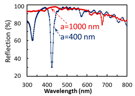
Figure 3.
Simulated reflection as a function of wavelength from Al-coated GPSC with periods of 1000 and 400 nm.
Figure 4a shows the E-field intensity in a cross-section in yz plane from the unit super-cell 12a × 12a of the GPSC. The GPSC is located at the bottom. In order to compare with the diffraction pattern excited by 532 nm laser, a source at 532 nm was incident toward GPSC from the top in the simulation. The E-field intensity was recorded at 100 time unit. Figure 4b shows the E-field intensity at the cross section in xy plane through z-location 1 in (a). The smaller the radius of the hole, the weaker the E-field intensity. At z-location 2, a constructive coupling occurs among beams from different holes along white arrows as shown in Figure 4c for the central region where holes are classified as two types of lattices as described in Figure 1c by arrows. The diffraction from (1,1) plane and the next nearest neighbor for Equation (3) can be understood from Figure 4c. Away from the center, the difference between the radii of holes becomes small. Thus, coupling can occur in x and y directions and E-field intensity shows orientations in x and y directions as indicated by red arrows in Figure 4c. Thus E-field intensity simulations indicate a coupling among fractional orders of Bloch waves. At z-location 3, the difference between E-field intensities in small and large holes becomes less than that at location 1 after coupling and re-distribution of E-field intensity at z-location 2. There are a total of 12 × 12 spots in Figure 4d corresponding to 12 × 12 fractional diffraction orders squared by (1,1), (1,−1), (−1,1) and (−1,−1) in Figure 2b and 12 × 12 fractional orders of momentum inside the first Brillouin zone in Figure 1d.
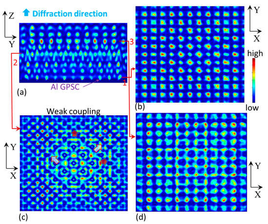
Figure 4.
(a) E-field intensity in a cross section in yz plane. (b–d) E-field intensity in a cross section in xy plane through z-location at 1, 2, and 3 labeled in (a), respectively.
5. Conclusions
Based on the multiple-beam interference, we have designed and fabricated GPSC with a gradual change of hole radii for two sets of lattices in GPSC and with a unit cell size of 12a × 12a. Over 1000 diffraction spots have been observed in the diffraction pattern from a 532 nm laser due to the fractional orders of momentum in the first Brillouin zone. The first order diffractions of (±1,0) or (0,±1) have disappeared due to the weak coupling between small and large holes. The high-order diffractions have been explained by the scattering from lattices and their next nearest neighbors. The simulation has shown the E-field intensity re-distribution between beams from small and large holes and the generation of 12 × 12 spots in the unit super-cell. These GPSCs can be used in solar cell, OLED or large area fluorescent lamp for lighting application.
Author Contributions
Y.L. and H.Z. conceived the concepts; Y.L. and S.H. designed simulations; S.H. and K.A. performed the simulations; N.H. performed pattern generation; S.H., Y.J. and U.P. performed E-beam and SEM experiments. Y.L., S.H. and N.H. analyzed the data and wrote the paper. All authors read and comment on the manuscript. All authors have read and agreed to the published version of the manuscript.
Funding
This work is supported by research grants from the U.S. National Science Foundation under Grant Nos. CMMI-1661842 and 1661749.
Conflicts of Interest
The authors declare no conflict of interest. The founding sponsors had no role in the design of the study; in the collection, analyses, or interpretation of data; in the writing of the manuscript, and in the decision to publish the results.
References
- Shechtman, D.; Blech, I.; Gratias, D.; Cahn, J.W. Metallic phase with long range orientational order and no translational symmetry. Phys. Rev. Lett. 1984, 53, 1951–1953. [Google Scholar] [CrossRef]
- Harb, A.; Torres, F.; Ohlinger, K.; Lin, Y.; Lozano, K.; Xu, D.; Chen, K.P. Holographically formed three-dimensional Penrose-type photonic quasicrystal through a lab-made single diffractive optical element. Opt. Express 2010, 18, 20512–20517. [Google Scholar] [CrossRef] [PubMed]
- Yu, N.; Genevet, P.; Kats, M.; Aieta, F.; Tetienne, J.; Capasso, F.; Gaburro, Z. Light propagation with phase discontinuities: Generalized laws of reflection and refraction. Science 2011, 334, 333. [Google Scholar] [CrossRef] [PubMed]
- Rybin, M.; Samusev, K.; Lukashenko, S.; Kivshar, Y.; Limonov, M. Transition from two-dimensional photonic crystals to dielectric metasurfaces in the optical diffraction with a fine structure. Sci. Rep. 2016, 6, 30773. [Google Scholar] [CrossRef]
- Sell, D.; Yang, J.; Doshay, S.; Yang, R.; Fan, J.A. Large-Angle, Multifunctional Metagratings Based on Freeform Multimode Geometries. Nano Lett. 2017, 17, 3752–3757. [Google Scholar] [CrossRef]
- Lutkenhaus, J.; George, D.; Moazzezi, M.; Philipose, U.; Lin, Y. Digitally tunable holographic lithography using a spatial light modulator as a programmable phase mask. Opt. Express 2013, 21, 26227–26235. [Google Scholar] [CrossRef]
- Lin, Y.; Herman, P.R.; Darmawikarta, K. Design and holographic fabrication of tetragonal and cubic photonic crystals with phase mask: Toward the mass-production of three-dimensional photonic crystals. Appl. Phys. Lett. 2005, 86, 071117. [Google Scholar] [CrossRef]
- Centeno, E.; Cassagne, D. Graded photonic crystals. Opt. Lett. 2005, 30, 2278–2280. [Google Scholar] [CrossRef]
- Do, K.; Roux, X.; Marris-Morini, D.; Vivien, L.; Cassan, E. Experimental demonstration of light bending at optical frequencies using a non-homogenizable graded photonic crystal. Opt. Express 2012, 20, 4776–4783. [Google Scholar] [CrossRef]
- Zhu, Q.; Jin, L.; Fu, Y. Graded index photonic crystals: A review. Ann. Phys. 2015, 527, 205–218. [Google Scholar] [CrossRef]
- Li, Y.; Fu, Y.; Minin, O.; Minin, I. Ultra-sharp nanofocusing of graded index photonic crystal-based lenses perforated with optimized single defect. Opt. Mater. Express 2016, 6, 2628–2636. [Google Scholar] [CrossRef]
- Lowell, D.; Lutkenhaus, J.; George, D.; Philipose, U.; Chen, B.; Lin, Y. Simultaneous direct holographic fabrication of photonic cavity and graded photonic lattice with dual periodicity, dual basis, and dual symmetry. Opt. Express 2017, 25, 14444–14452. [Google Scholar] [CrossRef] [PubMed]
- Lowell, D.; Hassan, S.; Adewole, M.; Philipose, U.; Chen, B.; Lin, Y. Holographic fabrication of graded photonic super-crystals using an integrated spatial light modulator and reflective optical element laser projection system. Appl. Opt. 2017, 56, 9888. [Google Scholar] [CrossRef]
- Hassan, S.; Sale, O.; Lowell, D.; Hurley, N.; Lin, Y. Holographic fabrication and optical property of graded photonic super-crystals with a rectangular unit super-cell. Photonics 2018, 5, 34. [Google Scholar] [CrossRef]
- Hassan, S.; Lowell, D.; Lin, Y. High light extraction efficiency into glass substrate in organic light-emitting diodes by patterning the cathode in graded superlattice with dual periodicity and dual basis. J. Appl. Phys. 2017, 121, 233104. [Google Scholar] [CrossRef]
- Hassan, S.; Alnasser, K.; Lowell, D.; Lin, Y. Effects of Photonic Band Structure and Unit Super-Cell Size in Graded Photonic Super-Crystal on Broadband Light Absorption in Silicon. Photonics 2019, 6, 50. [Google Scholar] [CrossRef]
- Hassan, S.; Sale, O.; Alnasser, K.; Hurley, N.; Zhang, H.; Philipose, U.; Lin, Y. Broadband light-matter interaction due to resonance cavities in graded photonic super-crystals. OSA Contin. 2019, 2, 3272–3280. [Google Scholar] [CrossRef]
- Jin, J.; Yin, X.; Ni, L.; Soljačić, M.; Zhen, B.; Peng, C. Topologically enabled ultrahigh-Q guided resonances robust to out-of-plane scatterin. Nature 2019, 574, 501. [Google Scholar] [CrossRef]
- Li, S.; Zhou, C.; Liu, T.; Xia, S. Symmetry-protected bound states in the continuum supported by all-dielectric metasurface. Phys. Rev. A 2019, 100, 063803. [Google Scholar] [CrossRef]
- Crawford, M.H. LEDs for Solid-State Lighting: Performance Challenges and Recent Advances. IEEE J. Sel. Top. Quantum Electron. 2009, 15, 1028–1040. [Google Scholar] [CrossRef]
- Singh, D.; Basu, C.; Meinhardt-Wollweber, M.; Roth, B. LEDs for energy efficient greenhouse lighting. Renew. Sustain. Energy Rev. 2015, 49, 139–147. [Google Scholar] [CrossRef]
- Kuo, T.; Ding, T.; Lin, J.; Ma, S. Optical Design of an LED Lighting Source for Fluorescence Microscopes. Appl. Sci. 2019, 9, 4574. [Google Scholar] [CrossRef]
- Rakic, A.; Djurisic, A.; Elazar, J.; Majewski, M. Optical properties of metallic films for vertical-cavity optoelectronic devices. Appl. Opt. 1998, 37, 5271. [Google Scholar] [CrossRef] [PubMed]
- Oskooi, F.; Roundy, D.; Ibanescu, M.; Bermel, P.; Joannopoulos, J.D.; Johnson, S.G. MEEP: A flexible free-software package for electromagnetic simulations by the FDTD method. Comput. Phys. Commun. 2010, 181, 687. [Google Scholar] [CrossRef]
- Ni, L.; Jin, J.; Peng, C.; Li, Z. Analytical and statistical investigation on structural fluctuations induced radiation in photonic crystal slabs. Opt. Express 2017, 25, 5580–5593. [Google Scholar] [CrossRef]
- Ohlinger, K.; Lutkenhaus, J.; Arigong, B.; Zhang, H.; Lin, Y. Spatially addressable design of gradient index structures through spatial light modulator based holographic lithography. J. Appl. Phys. 2013, 114, 213102–213108. [Google Scholar] [CrossRef]
- Hassan, S.; Lowell, D.; Adewole, M.; George, D.; Zhang, H.; Lin, Y. Extraordinary light trapping enhancement in silicon solar cell patterned with graded photonic super-crystal. Photonics 2017, 4, 50. [Google Scholar] [CrossRef]
- Alnasser, K.; Hassan, S.; Kamau, S.; Zhang, H.; Lin, Y. Enhanced light extraction from organic light emitting diodes by reducing plasmonic loss through graded photonic super-crystals. J. Opt. Soc. Am. B 2020, 37, 1283. [Google Scholar] [CrossRef]
- Nadell, C.C.; Huang, B.; Malof, J.M.; Padilla, W.J. Deep learning for accelerated all-dielectric metasurface design. Opt. Express 2019, 27, 27523–27535. [Google Scholar] [CrossRef]


© 2020 by the authors. Licensee MDPI, Basel, Switzerland. This article is an open access article distributed under the terms and conditions of the Creative Commons Attribution (CC BY) license (http://creativecommons.org/licenses/by/4.0/).