Communication

Ultra-Compact Power Splitters with Low Loss in Arbitrary Direction Based on Inverse Design Method

1
Guangxi Key Laboratory of Multimedia Communications and Network Technology, School of Computer, Electronics and Information, Guangxi University, Nanning 530004, China
2
Center of Material Science, National University of Defense Technology, Changsha 410073, China
*
Author to whom correspondence should be addressed.
Photonics 2021, 8(11), 516; https://doi.org/10.3390/photonics8110516
Submission received: 9 October 2021 / Revised: 11 November 2021 / Accepted: 14 November 2021 / Published: 16 November 2021

Abstract

:
The power splitter is a device that splits the energy from an input signal into multiple outputs with equal or uneven energy. Recently, the use of algorithms to intelligently design silicon-based photonic devices has attracted widespread attention. Thus, many optimization algorithms, which are called inverse design algorithms, have been proposed. In this paper, we use the Direct Binary Search (DBS) algorithm designed with three 1 × 3 power splitters with arbitrary directions theoretically. They have any direction and can be connected to other devices in any direction, which greatly reduces the space occupied by the optical integrated circuit. Through the simulation that comes about, we are able to get the insertion loss (IL) of the device we designed to be less than 5.55 dB, 5.49 dB, and 5.32 dB, separately. Then, the wavelength is 1530–1560 nm, so it can be used in the optical communication system. To discuss the impact of the footprint on device performance, we also designed another device with the same function as the second one from the above three devices. Its IL is less than 5.40 dB. Although it occupies a larger area, it has an advantage in IL. Through the design results, three 1 × 3 power splitters can be freely combined to realize any direction, multi-channel, ultra-compact power splitters, and can be better connected with different devices to achieve different functions. At the same time, we also show an example of a combination. The IL of each port of the combined 1 × 6 power splitter is less than 8.82 dB.

1. Introduction

With the rapid advancement of information, the replacement of electrical interconnection with optical interconnection is an inevitable trend to meet the speed and bandwidth requirements of massive information storage, rapid information transmission, and ultra-high-speed information processing. As an indispensable part of optical interconnection and optical communication systems, power splitters have attracted the attention of numerous researchers. In some traditional design methods, [1] proposed a traditional 1 × 8 splitter which has a lower correlation loss. However, the size of the device is 33 mm × 2.25 mm. A 1 × 2 waveguides splitter [2] is proposed dependent on the multimode interference (MMI) and photonic crystal. Moreover, the author of [3] designed a power splitter based on photonic crystal structure for photonic integrated circuits. Although these designs perform well, they all require manual adjustment of parameters, relying on the designer’s experience and intuition, which means that more manpower and time are required. In addition, the final device has a large footprint, which is inconvenient in practical applications [4,5]. In recent years, inverse design has attracted widespread attention due to its object-oriented design principles [6]. The essential thought of inverse design is to first determine the function of the final target device, and then use various optimization algorithms to calculate through the computer without manual participation, and finally calculate and design a device that meets the requirements. These seminal papers designed many nanophotonic devices with various functions [7,8,9,10]. They have employed advanced optimization methods. Currently, the commonly used optimization algorithms for micro-nano photonic devices are as follows: the direct-binary-search (DBS) algorithms [11,12,13], gradient-based optimization algorithm [14,15,16] and deep learning algorithm [17,18,19]. The design based on the gradient optimization algorithm is usually an irregular continuous shape [20]. Adjacent air pixels are prone to form etched areas of different shapes and different feature sizes, resulting in the lag effect [21], which brings challenges to sample manufacturing. Deep learning algorithm is broadly utilized within the design of micro-nano photonic devices [22]. The advantage of this method is that as long as the training is completed, the structure of the required target device can be found quickly, and can explore different possibilities more and get better solutions. However, there is a disadvantage that cannot be ignored. It requires a large number of data sets for training, which means a larger amount of calculation. At the same time, the network structure for training also needs to be explored to find a more suitable training network [23].
As a kind of intelligent optimization algorithm, the DBS algorithm is an iterative search algorithm that is applied to the design of nanophotonic devices [24]. The DBS algorithm has unparalleled advantages in realizing the design of on-chip micro-nano optical devices, due to its fast calculation speed, simple basic ideas, and convenient algorithm calculations. It can usually be applied to the design of a small parameter space [25]. At the same time, the digital element structure created by the DBS algorithm is more helpful for ensuing handling and fabrication. For example, a 2.6 μm × 2.6 μm ultra-compact 50:50 coupler [26] is designed using the DBS algorithm. Finally, the simulation results show that the IL of each port is less than 3.6 dB. As shown in [27], the photonic crystal-like sub-wavelength structure is shown. The device size is 2.72 μm × 2.72 μm. When the input light source is 1550 nm wavelength, the IL of the device is less than 3.2 dB. In addition, there are many power splitters with different functions and characteristics, which are optimized through algorithms, including 1 × 4 power splitter [28], power splitters with different ratios [29] etc. However, if these devices need to change the propagation direction, they need to be combined with waveguide bending, which undoubtedly increases the space occupied by the optical integrated circuit. The superposition of multiple devices will also affect the performance of the entire system. If power splitters with any direction can be designed, they can directly change the propagation direction of the on-chip beam after power splitting without adding additional waveguide bending. In this way, the final integration level of the photonic integrated circuit is higher, and the influence of excessive loss caused by the cascading of multiple devices is reduced. In the article [30], three 1 × 2 power splitters with any directions are proposed, which can be combined into power splitters with more output ports through their own combination. However, due to the limitation of the number of output ports, some output ports cannot be achieved with only 1 × 2 power splitters, such as 1 × 6 power splitters. In light of this, we use the DBS algorithm to design three different directions of 1 × 3 power splitters. They can also be combined with known 1 × 2 power splitters to achieve arbitrary channel and direction power splitters. When we use the optimized single device combination, it will inevitably lead to the degradation of device performance. Therefore, we also propose an optimization method that can improve the cascade of multiple devices. The goal is to use the optimized structure of a single device as the initial structure of the algorithm for further optimization. In this way, the on-chip beam can directly change the propagation direction after power splitting, without adding additional waveguide bending, and has excellent performance and compact structure. At the same time, the power splitter we designed can have a very compact size and better performance, which is beneficial to chip-level photonic integrated circuits. It plays a critical part within the dense integration, multi-function, and combined applications of micro-nano photonic devices.
In this paper, we designed the first 1 × 3 power splitter where the directions of the three output waveguides are all on the right side (RRRPS). In the second design of the 1 × 3 power splitter, two of the three output waveguides are on the bottom and one is on the left (LDDPS). The three output waveguides of the third 1 × 3 power splitter are in the left, right, and bottom directions (RLDPS). Moreover, through the combination of these devices, not only can it be combined into a power splitter with more channels, but it can also be interconnected with other devices to perform more functions. All of the footprints of the three devices are 2.4 μm × 2.4 μm. Finally, through simulation, the IL of the three devices is less than 5.55 dB, 5.49 dB, and 5.32 dB when the wavelength is 1530–1560 nm. Then we also use an example (LLDDPS) to illustrate the effect of size on the final performance. LLDDPS has expanded its footprint on the basis of LDDPS. The footprints of LLDDPS are 3.6 μm × 2.4 μm. The IL of each port is less than 5.40 dB. At the same time, we also show an example of a combination. The IL of each port of the combined 1 × 6 power splitter is less than 8.82 dB.

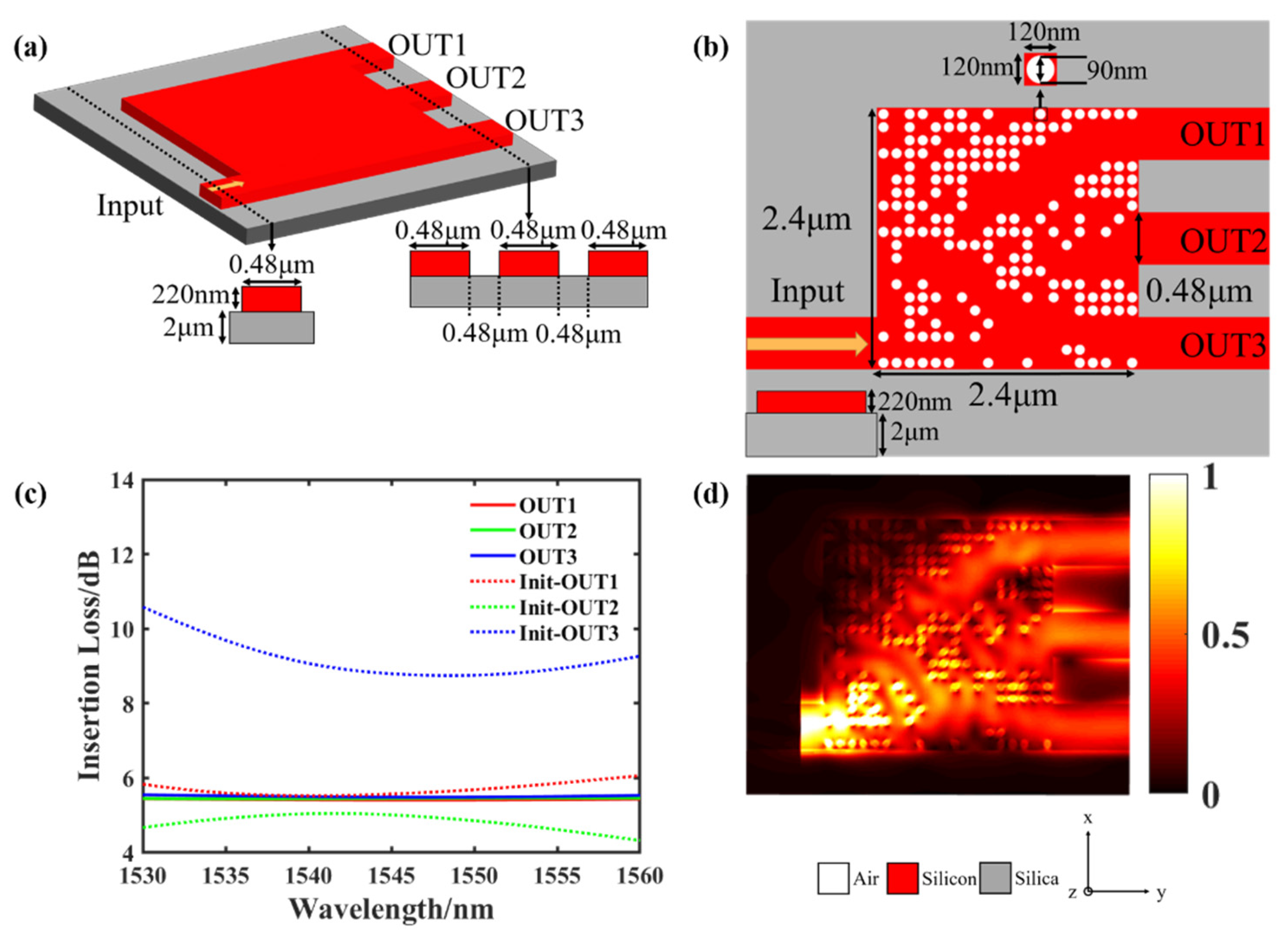
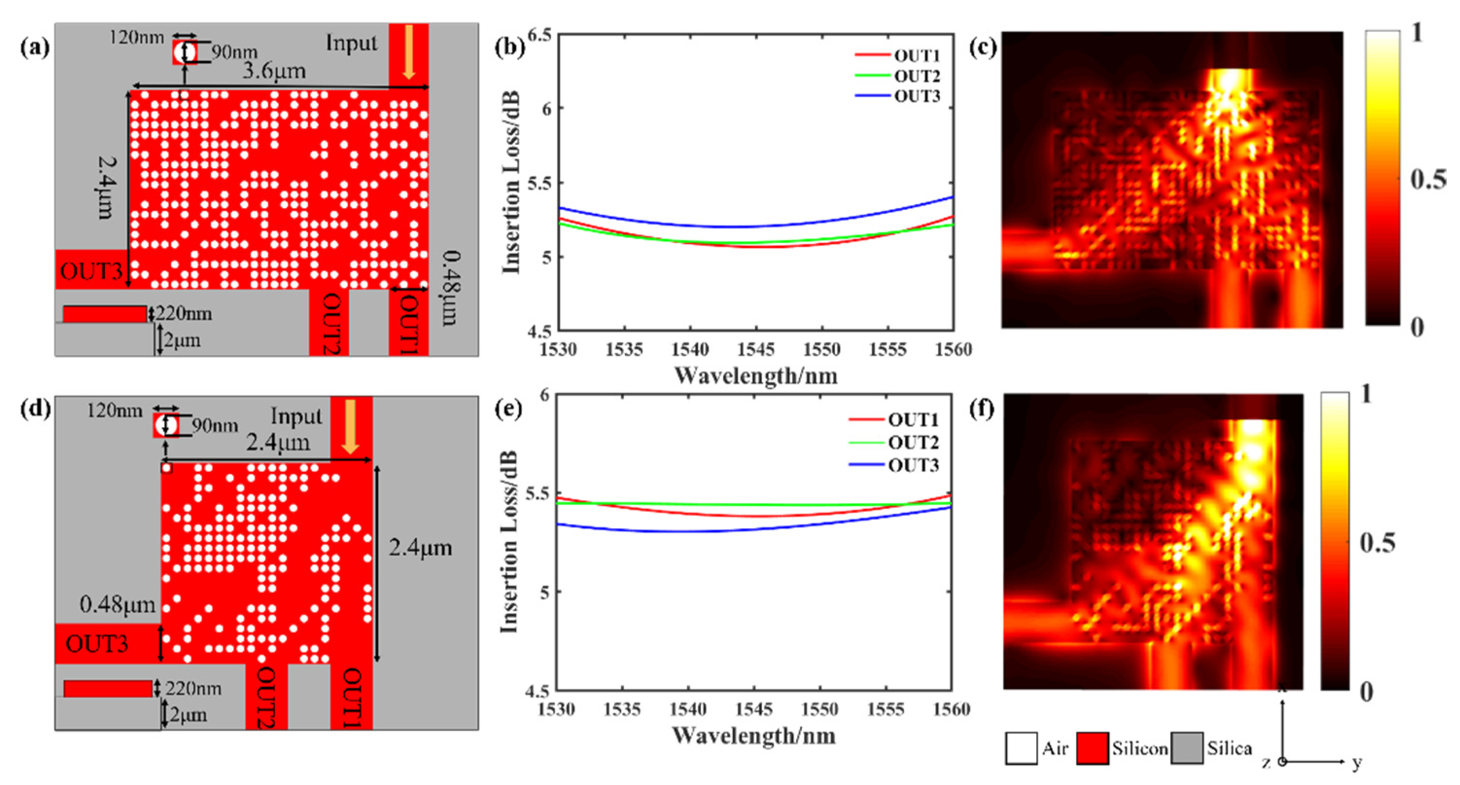
2. Methods and Results
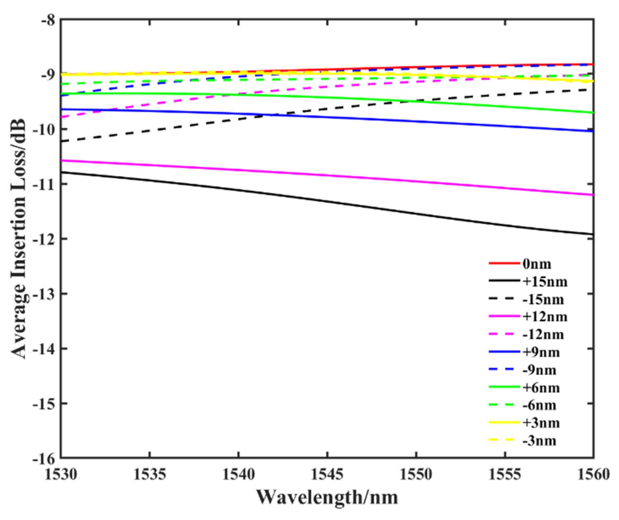
In this work, three 1 × 3 power splitters based on silicon-on-insulator (SOI) platforms with diverse output directions were shown by us. The method of the DBS algorithm can be separated into the following steps: First, divide the pixel points in the area that needs to be optimized, and each pixel point can be randomly set to ‘0’ or ‘1’, ‘1’ means silicon, ‘0’ means air. Then, set the figure-of-merit (FOM). Every time the state of a pixel is changed, a corresponding FOM can be obtained. In the event that the FOM has progressed, the state after the pixel flip is retained, otherwise, it returns to the state before the flip until all the pixels are traversed. This is called an iteration. The iterations continue until the FOM does not improve further.
For the first structure with three output ports in the same direction, we based it on SOI. The material parameters used are the top silicon thickness of 220 nm and the silicon dioxide buried layer thickness of 2 μm. The optimized region is 2.4 μm × 2.4 μm, and each pixel is set as a square with a side length of 120 nm, which is an empirical value [29]. The whole area is partitioned into 20 × 20 pixels. In order to make it easier to process the device into shape, we often use the robust design of manufacturing through the regularization constraints of the smallest gap and the smallest curvature [4]. To meet this requirement, we use the cylinder structure as the shape of the pixel block. The role of the circular hole is: After the light source is input from the input port, the circular hole can be used to influence the refractive index to adjust the light field [30]. When the adjacent pixel blocks are all etched, the air columns remain separated by the silicone sidewall between the air columns. All etched areas are independent of each other and have the same feature structure. The difference in this structure is to avoid the possible sharp corners [31] and the inconsistent etching depth brought about by the hysteresis effect [21]. When the state of the pixel is required to be ‘1’, it means that there is no etching, and it is indicated in red. When the pixel state is ‘0’, the diameter of the etched hole is 90 nm, and the etching depth is 220 nm, which we use white in the figure to indicate. The input wavelength is 1530–1560 nm, and the input light source mode is TE0. We use FDTD solutions to solve the issue, and finally determine the simulation mesh size at 30 nm. The initial configuration of the first structure is set as shown in Figure 1a. When optimizing, the output port is not as uniform as the 1 × 2 power splitter. Therefore, the unbalance factor of every port needs to be considered. We add a formula representing root-mean-square error (RMSE) to balance the value of the output port. The RMSE is the square root of the ratio of the square of the deviation between the predicted value and the true value to the number of observations, and is used to measure the deviation between the observed value and the true value. Here, our predicted value and observed value are expressed by the transmittance of two ports, respectively, indicating that we need to make the transmittance of each two ports have a lower difference. The expression is as follows:
R = [ ( t 1 t 2 ) 2 n ] 1 2 + [ ( t 1 t 3 ) 2 n ] 1 2 + [ ( t 2 t 3 ) 2 n ] 1 2
Here, t1, t2, and t3 individually refer to the transmittance of the three output wave-guides, and n represents the quantity of input wavelengths. The formula is the calculation of the transmittance of all wavelengths. The expression is to reduce the unbalance of the transmittance values of all wavelengths, and adjust the overall transmittance. Then we use a function M to represent the relationship of the transmittance of the three output ports, as shown below:
M = ( t 1 m i n + t 2 m i n + t 3 m i n ) ( | t 1 m i n t 2 m i n | + | t 1 m i n t 3 m i n | + | t 2 m i n t 3 m i n | )
Among them, t1min, t2min, and t3min respectively represent the minimum transmittance of all wavelengths in the corresponding port. The first half of the formula expresses the sum of the minimum transmittances of the three output ports, and the second half is the difference between the minimum transmittance of the three output ports. The purpose of our optimization is to increase the sum of the minimum transmittance and decrease the difference between the minimums. We need to increase the value of the function M, increase the transmittance of the output, and decrease the value of R, to achieve the goal of balancing the output of the three ports as much as possible. Considering the above factors, the FOM we finally set is defined as:
FOM = α × ( t 1 m i n + t 2 m i n + t 3 m i n ) β × ( | t 1 m i n t 2 m i n | + | t 1 m i n t 3 m i n | + | t 2 m i n t 3 m i n | ) γ × [ ( t 1 t 2 ) 2 n ] 1 2 + [ ( t 1 t 3 ) 2 n ] 1 2 + [ ( t 2 t 3 ) 2 n ] 1 2
Then α, β and γ are used by us to represent the weight coefficient of each small item in R and M, respectively. Here, α + β + γ = 1, and they are set to 0.8, 0.1 and 0.1, respectively [32]. When the FOM no longer improves, the iteration stops. It takes~9 h on average to get the final results after 4 iterations. The ultimate optimized structure appears in Figure 1b. At the same time, we set IL to represent the insertion loss of each output waveguide [26]:
IL m = 10 × log ( t m T )
In the formula, tm is the transmittance of each output waveguide, and T is the total transmittance of the input waveguide. Moreover, m addresses the quantity of output ports. In particular, Figure 1c shows a comparison chart of the insertion loss before and after optimization of the device. We can see that the output of the first three output ports is very unbalanced, and the results we want are not achieved. After optimization, it can be seen that the output of the three ports is very balanced and achieves the desired 1 × 3 power splitting effect. It tends to be seen that when the wavelength is 1530–1560 nm, the insertion loss of each output waveguide is below 5.55 dB. Then we can see from the optical field distribution diagram of the RRRPS in Figure 1d that the device has achieved the effect of power distribution.
For the FOM in Equation (3), the α term represents the weight of the sum of the minimum transmittances of the three output channels. Our ultimate goal of this optimization is to make the transmittance as high as possible, so the weight of this item should be the highest. At the same time, we also need to consider the port imbalance. Since the two items are adjustment items for the degree of imbalance, we fixed γ = 0.1, and then discussed α/β. It can be seen from Figure 2a that the final average insertion loss does decrease as the weight of α increases, which is the desired result. At the same time, we have also added Figure 2b to show the changes in port imbalance. Finally, we selected the ratio α/β = 0.8/0.1 that has the best transmittance and the centered port imbalance.
In addition, we designed a second power splitter (LDDPS) and demonstrated another larger device (LLDDPS) with the same function for comparison and discussion. Figure 3a is the optimized structure. The footprint of LLDDPS is 3.6 μm × 2.4 μm. The distance between the two output waveguides at the bottom is 0.48 μm. In Figure 3c, the light field distribution of the final simulation is shown. Finally, it can be seen from Figure 3b that the IL of each output port is below 5.40 dB. Then the final structure with a footprint of only 2.4 μm × 2.4 μm and the simulated square distribution is shown in Figure 3d,f, respectively. The final IL is less than 5.49 dB in Figure 3e. It is well known that as the refractive index or shape of the waveguide changes, the propagation direction of light, power splitting, and other characteristics will also change. We can therefore control the local refractive index to guide the light to the direction of the output port [33]. In the DBS algorithm, the refractive index is affected by searching for the appropriate pixel distribution to adjust the light field. A smaller footprint will result in a reduction in the number of pixels, and the control ability of pixel distribution will also be weakened. Therefore, reducing the footprint will affect the performance. Through the analysis of the results, increasing the footprint will improve the performance. Depending on the actual situation, if a smaller size is required, then there may be a decrease in performance. If you choose better performance, you must accept larger sizes.
For the third power splitter (LRDPS), we can use the symmetrical structure for optimization. As shown in Figure 4a, we only need to optimize half of the region, and then get the structure of the other part of the region by axial symmetry. Through this method, we can reduce the time for optimization calculations. In Figure 4b, the ultimate structure after LRDPS optimization appears. It tends to be seen in Figure 4c that in the range of wavelengths 1530–1560 nm, the IL of each output waveguide is below 5.32 dB. The ultimate optical field distribution graph appears in Figure 4d.

3. Discussion

After the optimization of the 1 × 3 power splitters in different output directions is completed, they can be combined according to actual needs. When we combine the design with the optimized 1 × 2 power splitter in [30], we can realize the power splitter of any channel. Due to the many ways of combination, here we show a 1 × 6 power splitter. We begin by basically combining the known 1 × 2 power splitter and RRRPS and then further optimize the simulation. Figure 5a shows the structure after our final optimization, and Figure 5b shows the light field distribution. In Figure 5c, we are able to see that the IL of each port is less than 8.82 dB at the conclusion, and the output that comes out of each output port is exceptionally uniform. In Figure 5d, we show the initial IL of the known 1 × 2 power splitter. At the same time, the average insertion loss of the device after simple combination is compared with the average insertion loss after further optimization. It can be seen that by further optimizing this method by taking the structure of the device after simple combination as the initial structure, the performance of the device can be greatly improved. Our method of optimizing the combined equipment improves the performance of the assembled equipment and very well may be all the more broadly utilized within the design of micro-nano photonic devices. In Table 1, we show a comparison with other work. It can be seen that we have an advantage in terms of footprint. At the same time, our work also has diversified directions, consideration of cascading, and scalability.
We will process the device in the follow-up work. We can use E-Beam Lithography (EBL) equipment to fabricate SOI devices. Then, inductively coupled plasma etching (Inductive Coupled Plasma-Reactive Ion Etching, ICP-RIE) equipment is used to transfer the mask to the silicon device layer [37]. It mainly includes the following steps: SOI wafer pretreatment, deposition of silicon and silicon layers, spin coating of the adhesion layer, negative photoresist and conductive layer, E-Beam exposure, development, etching and photoresist removal. [38,39,40]. Finally, it can be detected by vertical coupling test [14]. Since there are unavoidable random manufacturing defects in actual operation, the manufacturing tolerances must be considered. Here, we simulated the performance changes of the device in several different diameter ranges, and drew the average insertion loss graph for comparison. We can see from the comparison in Figure 6, when the diameter changes at +12 nm, the average insertion loss of the device has begun to have a more obvious deviation. It reaches a maximum of +15 nm. The maximum tolerable manufacturing tolerance of this device is 12 nm. When this accuracy is exceeded, the performance of the device is greatly affected. At the same time, the accuracy of EBL can be very small (about 8 nm). It can be seen from this maximum manufacturing tolerance that our devices can be manufactured very well.

4. Conclusions

In this paper, we list three ultra-compact and low-loss 1 × 3 power splitters with arbitrary input and output directions. They have the same compact sizes of 2.4 μm × 2.4 μm, and the insertion loss of each device is less than 5.55 dB, 5.49 dB, and 5.32 dB, respectively. We have also described another device that has the same function as the second version of the above three devices. Although its footprint is 3.6 μm × 2.4 μm, it has a lower IL, less than 5.40 dB. Through the design of power splitters with different outputs in different directions, these initial structures can be further combined to reach more output ports of power splitters. We show a 1 × 6 power splitter with an IL less than 8.82 dB. At the same time, these devices can not only be combined with themselves, but also can be better combined with other devices to achieve more functions, and further provide greater contributions to the optical interconnection system.

Author Contributions

Y.X. and H.M. contributed to the idea. Y.X. designed and performed the analysis, and prepared the figures/tables. H.M. and T.X. contributed to manuscript preparation. Z.Z. and J.Y. conceived and guided the research and supervised the work. All authors have read and agreed to the published version of the manuscript.

Funding

Project supported by National Natural Science Foundation of China (61661004); Guangxi Science Key Research and Development Project (Guangxi Science AB1850043); Program for New Century Excellent Talents in University (NCET-12-0142); Natural Science Foundation of Hunan Province (13JJ3001); China Postdoctoral Science Foundation (2018M633704); National Natural Science Foundation of China (60907003, 61805278); the Foundation of NUDT (JC13-02-13, ZK17-03-01).

Institutional Review Board Statement

Not applicable.

Informed Consent Statement

Not applicable.

Data Availability Statement

Data are available in the main text.

Conflicts of Interest

The authors declare no conflict of interest.

References

  1. Gamet, J.; Pandraud, G. Ultralow-Loss 1 Times 8 Splitter Based on Field Matching Y Junction. IEEE Photonics Technol. Lett. 2004, 16, 2060–2062. [Google Scholar] [CrossRef]
  2. Tao, L.; Zakharian, A.R.; Fallahi, M.; Moloney, J.V.; Mansuripur, M. Multimode Interference-Based Photonic Crystal Waveguide Power Splitter. J. Lightwave Technol. 2004, 22, 2842–2846. [Google Scholar]
  3. Park, I.; Lee, H.S.; Kim, H.J.; Moon, K.M.; Lee, E.H. Photonic Crystal Power-Splitter Based on Directional Coupling. Opt. Express 2004, 12, 3599–3604. [Google Scholar] [CrossRef] [PubMed]
  4. Piggott, A.Y.; Petykiewicz, J.; Su, L.; Vu Kovi, J. Fabrication-Constrained Nanophotonic Inverse Design. Sci. Rep. 2017, 7, 1786. [Google Scholar] [CrossRef] [Green Version]
  5. Lu, J.; Vučković, J. Nanophotonic computational design. Opt. Express 2013, 21, 13351–13367. [Google Scholar] [CrossRef] [PubMed]
  6. Molesky, S.; Lin, Z.; Piggott, A.Y.; Jin, W.; Vucković, J.; Rodriguez, A.W. Jelena Inverse Design in Nanophotonics. Nat. Photonics 2018, 12, 659–670. [Google Scholar] [CrossRef] [Green Version]
  7. Jiao, Y.; Fan, S.; Miller, D. Demonstration of Systematic Photonic Crystal Device Design and Optimization by Low-Rank Adjustments: An Extremely Compact Mode Separator. Opt. Lett. 2005, 30, 141–143. [Google Scholar] [CrossRef]
  8. Piggott, A.Y.; Lu, J.; Lagoudakis, K.G.; Petykiewicz, J.; Babinec, T.M.; Vukovi, J. Inverse Design and Demonstration of a Compact and Broadband On-Chip Wavelength Demultiplexer. Nat. Photonics 2015, 9, 374–377. [Google Scholar] [CrossRef] [Green Version]
  9. Shen, B.; Wang, P.; Polson, R.; Menon, R. Rajesh an Integrated-Nanophotonics Polarization Beamsplitter with 2.4 × 2.4 Mm2 Footprint. Nat. Photonics 2015, 9, 378–382. [Google Scholar] [CrossRef]
  10. Jensen, J.S.; Sigmund, O. Topology Optimization for Nano-Photonics. Laser Photonics Rev. 2011, 5, 308–321. [Google Scholar] [CrossRef]
  11. Liu, Y.; Xu, K.; Wang, S.; Shen, W.; Xie, H.; Wang, Y.; Xiao, S.; Yao, Y.; Du, J.; He, Z.; et al. Arbitrarily Routed Mode-Division Multiplexed Photonic Circuits for Dense Integration. Nat. Commun. 2019, 10, 3263. [Google Scholar] [CrossRef] [Green Version]
  12. Shen, B.; Polson, R.; Menon, R. Increasing the Density of Passive Photonic-Integrated Circuits Via Nanophotonic Cloaking. Nat. Commun. 2016, 7, 13126. [Google Scholar] [CrossRef]
  13. Yu, Z.; Cui, H.; Sun, X. Genetically Optimized On-Chip Wideband Ultracompact Reflectors and Fabry–Perot Cavities. Photonics Res. 2017, 5, B15–B19. [Google Scholar] [CrossRef]
  14. Liu, Z.; Liu, X.; Xiao, Z.; Lu, C.; Zhang, X. Integrated Nanophotonic Wavelength Router Based on an Intelligent Algorithm. Optica 2019, 6, 1367. [Google Scholar] [CrossRef]
  15. Davis, A.J.; Hahlweg, C.F.; Mulley, J.R.; Callewaert, F.; Aydin, K. Inverse-designed all-dielectric waveguide bend. In Proceedings of the Novel Optical Systems Design & Optimization XIX, San Diego, CA, USA, 29–31 August 2016; p. 99480Q. [Google Scholar]
  16. Huang, J.; Yang, J.; Chen, D.; He, X.; Han, Y.; Zhang, J.; Zhang, Z. HAN Ultra-Compact Broadband Polarization Beam Splitter with Strong Expansibility. Photonics Res. 2018, 6, 574–578. [Google Scholar] [CrossRef]
  17. Nadell, C.C.; Huang, B.; Malof, J.M.; Padilla, W.J. Deep Learning for Accelerated All-Dielectric Metasurface Design. Opt. Express 2019, 27, 27523. [Google Scholar] [CrossRef]
  18. Liu, D.; Tan, Y.; Khoram, E.; Yu, Z. Training Deep Neural Networks for the Inverse Design of Nanophotonic Structures. ACS Photonics 2018, 5, 1365–1369. [Google Scholar] [CrossRef] [Green Version]
  19. Del Hougne, P.; Imani, M.F.; Diebold, A.V.; Horstmeyer, R.; Smith, D.R. Learned Integrated Sensing Pipeline: Reconfigurable Metasurface Transceivers as Trainable Physical Layer in an Artificial Neural Network. Adv. Sci. 2020, 7, 1901913. [Google Scholar] [CrossRef] [Green Version]
  20. Su, L.; Piggott, A.Y.; Sapra, N.V.; Petykiewicz, J.; Vu Kovi, J. Inverse Design and Demonstration of a Compact On-Chip Narrowband Three-Channel Wavelength Demultiplexer. ACS Photonics 2017, 5, 301–305. [Google Scholar] [CrossRef] [Green Version]
  21. Chang, W.; Xu, S.; Cheng, M.; Liu, D.; Zhang, M. Inverse Design of Single-Step-Etched Ultracompact Silicon Polarization Rotator. Opt. Express 2020, 28, 28343–28351. [Google Scholar] [CrossRef]
  22. Tahersima, M.H.; Kojima, K.; Koike-Akino, T.; Jha, D.; Wang, B.; Lin, C.; Parsons, K. Deep Neural Network Inverse Design of Integrated Photonic Power Splitters. Sci. Rep. 2019, 9, 1–9. [Google Scholar]
  23. Huang, J.; Ma, H.; Chen, D.; Yuan, H.; Zhang, J.; Li, Z.; Han, J.; Wu, J.; Yang, J. Digital Nanophotonics: The Highway to the Integration of Subwavelength-Scale Photonics: Ultra-Compact, Multi-Function Nanophotonic Design Based on Computational Inverse Design. Nanophotonics 2021, 10, 1011–1030. [Google Scholar] [CrossRef]
  24. Chhetri, B.B.; Yang, S.; Shimomura, T. Stochastic Approach in the Efficient Design of the Direct-Binary-Search Algorithm for Hologram Synthesis. Appl. Opt. 2000, 39, 5956–5964. [Google Scholar] [CrossRef]
  25. Ma, L.; Li, J.; Liu, Z.; Zhang, Y.; Zhang, N.; Zheng, S.; Lu, C. Intelligent Algorithms: New Avenues for Designing Nanophotonic Devices. Chin. Opt. Lett. 2021, 19, 011301. [Google Scholar] [CrossRef]
  26. Zhang, M.; Lu, L.; Zhou, F.; Liu, D. An Ultra-compact Colorless 50:50 Coupler Based on PhC-like Metamaterial Structure. In Proceedings of the 2016 Optical Fiber Communications Conference & Exhibition, Anaheim, CA, USA, 20–24 March 2016. [Google Scholar]
  27. Lu, L.; Liu, D.; Zhou, F.; Li, D.; Cheng, M.; Deng, L.; Fu, S.; Xia, J.; Zhang, M. Inverse-Designed Single-Step-Etched Colorless 3 dB Couplers Based On RIE-lag-insensitive PhC-like Subwavelength Structures. Opt. Lett. 2016, 41, 5051–5054. [Google Scholar] [CrossRef] [PubMed]
  28. Xie, H.; Liu, Y.; Sun, W.; Wang, Y.; Ke, X.; Du, J.; He, Z.; Song, Q. Inversely Designed 1 × 4 Power Splitter with Arbitrary Ratios at 2-Mm Spectral Band. IEEE Photonics J. 2018, 10, 1–6. [Google Scholar] [CrossRef]
  29. Ke, X.; Lu, L.; Xiang, W.; Sun, W.; Song, Q. Integrated Photonic Power Divider with Arbitrary Power Ratios. Opt. Lett. 2017, 42, 855. [Google Scholar]
  30. Ma, H.; Huang, J.; Zhang, K.; Yang, J. Arbitrary-Direction, Multichannel and Ultra-Compact Power Splitters by Inverse Design Method. Opt. Commun. 2020, 462, 125329. [Google Scholar] [CrossRef]
  31. Abrokwah, K.O. Characterization and Modeling of Plasma Etch Pattern Dependencies in Integrated Circuits; Massachusetts Institute of Technology: Cambridge, MA, USA, 2006; pp. 106–107. [Google Scholar]
  32. Ma, H.; Huang, J.; Zhang, K.; Yang, J. Inverse-Designed Arbitrary-Input and Ultra-Compact 1 × N Power Splitters Based on High Symmetric Structure. Sci. Rep. 2020, 10, 11757. [Google Scholar] [CrossRef]
  33. Shen, B.; Peng, W.; Polson, R.; Menon, R. Integrated Metamaterials for Efficient and Compact Free-Space-To-Waveguide Coupling. Opt. Express 2014, 22, 27175–27182. [Google Scholar] [CrossRef]
  34. Rashed, A.M.; Selviah, D.R. Modeling of a Polymer 1 × 3 MMI Power Splitter for Optical Backplane. In Proceedings of the Conference on Optoelectronic and Microelectronic Materials and Devices, Brisbane, QLD, Australia, 8–10 December 2004; pp. 281–284. [Google Scholar]
  35. Piggott, A.Y.; Ma, E.Y.; Su, L.; Ahn, G.H.; Sapra, N.V.; Vercruysse, D.; Netherton, A.M.; Khope, A.S.P.; Bowers, J.E.; Vučković, J. Inverse-Designed Photonics for Semiconductor Foundries. ACS Photonics 2020, 7, 569–575. [Google Scholar] [CrossRef]
  36. Meng, C.; Qiu, J.; Tian, Y.; Ye, Z.; Wu, J. A broadband compact 1 × 3 power splitter designed with inverse design method. In Proceedings of the 2016 15th International Conference on Optical Communications and Networks (ICOCN), Hangzhou, China, 24–27 September 2016. [Google Scholar]
  37. Lu, L.; Zhang, M.; Zhou, F.; Chang, W.; Tang, J.; Li, D.; Liu, D. Inverse-designed ultra-compact star-crossings based on PhC-like subwavelength structures for optical intercross connect. Opt. Express 2017, 25, 18355–18364. [Google Scholar] [CrossRef] [PubMed]
  38. Tao, S.H.; Fang, Q.; Song, J.F.; Yu, M.B.; Kwong, D.L. Cascade Wide-Angle Y-junction 1 × 16 Optical Power Splitter Based on Silicon Wire Waveguides on Silicon-On-Insulator. Opt. Express 2008, 16, 21456–21461. [Google Scholar] [CrossRef] [PubMed]
  39. Borel, P.I.; Frandsen, L.H.; Harp Th, A.; Kristensen, M.; Jensen, J.S.; Sigmund, O. Topology Optimised Broadband Photonic Crystal Y-splitter. Electron. Lett. 2005, 41, 69–71. [Google Scholar] [CrossRef]
  40. Wright, D.; Galarre Ta, C.; Sinev, I.; Alexeev, A.M.; Bertolotti, J. Selective Reconfigurable Multilevel Control of Resonant Modes in Hybrid All-Dielectric/Phase-Change Metasurfaces. Optica 2020, 7, 476–484. [Google Scholar]
Figure 1. The simulated results of RRRPS. (a) Initial structure before optimization. (b) The final structure after optimization. (c) is a comparison chart of the insertion loss before and after optimization of RRRPS. (d) Simulated optical field distributions.
Photonics 08 00516 g001
Figure 2. The effect of different weights changes on device performance. (a) The average insertion loss of the three output ports beneath different weights. (b) The average insertion loss imbalance of the three output ports beneath different weights.
Photonics 08 00516 g002
Figure 3. The simulated results of LLDDPS and LDDPS. (a,d) are the final simulation structure. (b,e) are the IL of each output waveguide of LLDDPS and LDDPS, respectively. (c,f) are the optical field distribution.
Photonics 08 00516 g003
Figure 4. The simulated results of LRDPS. (a) Initial structure before optimization. (b) The final structure after optimization. (c) are the IL of each port of LRDPS. (d) Simulated optical field distributions.
Photonics 08 00516 g004
Figure 5. The simulated results of 1 × 6 power splitter. (a) The final structure after optimization. (b) are the IL of each port. (c) Simulated optical field distributions. (d) The 1 × 2 power splitter’s average insertion loss after initial IL and simple combination was compared with the average insertion loss after further optimization.
Photonics 08 00516 g005
Figure 6. The simulated results under the diameter variations.
Photonics 08 00516 g006
Table 1. Comparison of other works.
ReferencesFootprintIL (EL [33])Direction (Directly Change the Propagation Direction after Power Splitting, without Adding Additional Waveguide Bending)Cascading Combinations (after the Devices are Cascaded, the Performance Will Be Improved after Further Optimization)Scalability (Combination to Realize 1 × N Power Splitter in Any Direction)
This Work2.4 × 2.4 μm5.55 dB (0.69 dB)Directional flexibilityYesYes
5.49 dB (0.63 dB)
5.32 dB (0.48 dB)
[34]23 × 292 μm(0.4 dB)Single directionNoNo
[4]3.8 × 2.5 μm(0.642 dB)Single directionNoNo
[35]3.8 × 2.5 μm(0.4 dB)Single directionNoNo
[36]2.8 × 2.8 μm(0.49 dB)Single directionNoNo
Publisher’s Note: MDPI stays neutral with regard to jurisdictional claims in published maps and institutional affiliations.

