Article

Experimental Investigation on the Sputtering Process for Tantalum Oxynitride Thin Films

1
Department of Biomedical Engineering, National Yang Ming Chiao Tung University, Taipei 11221, Taiwan
2
Department of Mechanical Engineering, National Central University, Jhongli, Taoyuan 32001, Taiwan
3
Department of Materials Engineering, Ming Chi University of Technology, Taishan, Taipei 24301, Taiwan
*
Author to whom correspondence should be addressed.
Photonics 2021, 8(2), 53; https://doi.org/10.3390/photonics8020053
Submission received: 2 January 2021 / Revised: 2 February 2021 / Accepted: 11 February 2021 / Published: 15 February 2021
(This article belongs to the Special Issue Photonic Devices and Systems)

Abstract

:
Metal oxynitrides are compounds between nitrides and oxides with a certain level of photocatalytic functions. The purpose of this study is to investigate an appropriate range of oxygen flow rate during sputtering for depositing tantalum oxynitride films. The sputtering process was carried out under fixed nitrogen but variable oxygen flow rates. Post rapid thermal annealing was conducted at 800 °C for 5 min to transform the as-deposited amorphous films into crystalline phases. The material characterizations of annealed films include X-ray diffraction and Raman spectroscopy for identifying crystal structures; scanning electron microscope for examining surface morphology; energy-dispersive X-ray spectroscopy to determine surface elemental compositions; four-point probe and Hall effect analysis to evaluate electrical resistivity; UV-visible-NIR spectroscopy for quantifying optical properties and optical bandgaps. To assess the photocatalytic function of oxynitride films, the degradation of methyl orange in de-ionized water was examined under continuous irradiation by a simulated solar light source for six hours. Results indicate that crystalline tantalum oxynitride films can be obtained if the O2 flow rate is chosen to be 0.25–1.5 sccm along with 10 sccm of N2 and 20 sccm of Ar. In particular, films deposited between 0.25 and 1.5 sccm O2 flow have higher efficiency in photodegradation on methyl orange due to a more comprehensive formation of oxynitrides.

1. Introduction

Certain transition metal oxynitrides are known photocatalysts capable of water splitting by the energy of photons in the range of visible light [1,2,3]. The photocatalytic function relies on two material characters; one is the multivalence of the metallic element which is intrinsic to transition-metals, and the other is hybridized orbitals between metals and oxygen or nitrogen to provide intra-bands between valance and conduction bands. Much more like doping processes, these intra-bands not only provide alternative paths for electrons to change their states but also serve as stepstones to the conduction band. If prudently articulating this mechanism, the electron-hole pair can be effectively separated and followed by further immediately available proximate photochemical reactions.
From an engineering point of view, transition metal oxynitrides can be apt photo-catalysts only under given optimal compositions and microstructures. Another feature of transition metal oxynitrides is their good corrosive resistance because of the stable microstructures maintained by the coexistence of nitrides and oxides [1,2,3]. This is an additive favorite for oxynitrides as catalysts without compromising integrity in harsh conditions. In general, oxynitrides are more stable under atmospheric and aqueous conditions when compared to pure nitrides due to the presence of oxide phases. This feature provides an advantage for applications that require continuous operations under oxidative environments or submersion in aqueous solutions, such as water splitting or environmental treatment [1]. Metal oxynitrides are also mechanically stronger than pure oxides because of denser structures packed by nitrides [4,5,6].
The optical band gaps in many transition-metal oxynitrides are narrower than those of pure oxides [1,3,7,8,9,10,11]. For example, the generic band gap of TiO2 is ~3.2 eV, which corresponds to ~387 nm wavelength, while an N-doping of TiO2 has a bandgap reduced from the ultraviolet into the visible region (<3.1 eV, of wavelength 399.95 nm) ready for photocatalysis [12,13,14,15]. The smaller bandgap makes transition metal oxynitrides electronically and optically advantageous. Moreover, for materials to be practically useful, these oxynitrides usually have high valences in the d0 orbital configuration in order to have copious electrons available, leading to some unique electrical, optical, or even magnetic properties. Such a setting also characteristically forms the crystal structure of AB(NxO3-x), where both A and B are transition metals. Examples of these oxynitrides are LaTaON2 and BaTaO2N, just to name a few [8,16,17,18,19].
More particulars about the optical band gap in transition metal oxynitrides are briefly discussed here. Since oxygen is more electronically negative than nitrogen (O2: ( σ 2 s ) 2 ( σ 2 s * ) 2 ( σ 2 p ) 2 ( π 2 p ) 4 ( π 2 p * ) 2 vs. N2: ( σ 2 s ) 2 ( σ 2 s * ) 2 ( σ 2 p ) 2 ( π 2 p ) 4 ), the energy level of hybrid orbitals between transition metals and oxygen is lower than that between metals and nitrogen. This affects the valance bands in pure oxides to be lower as compared to those in pure nitride. The lower valance band thus leads to a larger bandgap as the valance band is anion-based (O or N dominant), while the conduction band is cation-based (metal dominant). Therefore, introducing nitrides in pure oxides (nitridation) can be a viable approach to reduce the typical wide bandgaps in oxides. The narrower bandgap is also a prerequisite for photocatalytic function in the range of visible light region (λ = 400–700 nm).
However, from the manufacturing aspect, nitridation on oxides is a more demanding process that usually requires high temperature or pressure with a large supply of nitrogen because oxides are chemically much more stable than nitrides. On the contrary, with a much smaller amount of oxygen, oxidation of nitrides is a more viable and precise way to create oxynitrides as the chemically active characters of oxygen. It is also important to remember that the photocatalytic function critically relies on the delicate ratio of microstructures between nitrides and oxides [20,21,22,23,24,25,26].
In this study, we deposited tantalum oxynitride films by sputtering under fixed nitrogen (10 sccm) and variable oxygen flow rates (0–4 sccm). Tantalum is a rare transition metal and is highly corrosion-resistant due to its chemical inertness. It is also a refractory metal with a melting point of 3290 K (3017 °C). Tantalum belongs to the d-block group in the periodic table and is of multivalence with possible oxidation states of −3, −1, +1, +2, +3, +4, and +5 (naturally stable state) [27,28]. All these properties are compatible with the purpose of photo-catalysis.
To have crystalline films, rapid thermal annealing was further carried out after deposition to form crystalline tantalum oxynitride. The material characterizations on films include X-ray diffraction (XRD) for identifying crystal structures in annealed films, scanning electron microscope (SEM) for observing surface morphologies, energy-dispersive X-ray spectroscopy (EDS) for checking surface elemental compositions, Raman Spectroscopy for identifying vibrational modes in crystal structures, four-point probe, and Hall effect analyzer for evaluating electrical conductivity, and UV-visible-NIR spectrometer for the optical absorption and transparency. Optical band gaps of deposited films were numerically estimated using the Tauc plot based on UV-visible-NIR spectroscopy. After the aforementioned characterizations, the photodegradation efficiency of selected films was tested against methyl orange in de-ionized (DI) water under continuous exposure to visible light for a prolonged period.

2. Experiment

The tantalum oxynitride thin films are deposited by sputtering on quartz glass (20 mm × 20 mm × 0.7 mm, for optical measurements) or Si wafer (ϕ 4”, p-type, 20 mm × 20 mm × 0.5 mm, for material characterizations). Details of sputtering and measurement of films shall be discussed in the following. The experimental outline and parameters of sputtering are presented in Figure 1 and Table 1, respectively, for readers’ reference.

2.1. Substrate Preparation

A 4" silicon wafer (p-type, <100>) was first cut into 20 mm × 20 mm pieces using a diamond scribe. The cut substrate was etched in buffered oxide etchant (6:1 volume ratio of 40% NH4F in water to 49% of HF in water) for 20~30 seconds to remove silicon dioxide (SiO2) or silicon nitride (Si3N4). After etching, the sample was ultrasonically cleaned following the sequence of de-ionized (DI) water, acetone (100%), (DI) water, ethanol (95%), and DI water, each lasting for 10 minutes. Finally, the substrates were blown dry in nitrogen (99.95%).
For quartz glass (99.99%, Ultimate Materials Technology Co., Ltd. Hsinchu, Taiwan), it was also cut into 20 mm × 20 mm pieces using a diamond scribe. Then, the cut glass was ultrasonically cleaned by KOH (1 g/100ml in water) and the same sequence of the aforementioned solutions for 10 minutes each. Similarly, the substrates were blown dry in nitrogen (99.95%).

2.2. Film Deposition

Tantalum targets (99.99 wt.% Ultimate Materials Technology Co., Ltd. Hsinchu, Taiwan) and parameters used for the deposition of different films are listed in Table 1. The PVD chamber before the deposition was vacuumed to 6.4×10⁻⁴ Pa under room temperature for all depositions. The working gases for plasma were 20 sccm Ar (99.999%), 10 sccm N2 (99.999%), and/or O2 (99.999%) at various flow rates. All gases were purchased from local suppliers. The flow rates of all gases were controlled by mass flow controllers installed at the outlet of gas tanks. All mass flow controllers were also purchased from local suppliers.
Direct current (DC) power of 190 W is supplied to the Ta target. No substrate bias is applied during deposition.
To clean up volatile contaminants on the target, we always pumped Ar into the chamber at first and maintained it for 10 minutes before the deposition. All other process parameters can be found in Table 1 without further elaboration.
Post-deposition annealing is carried out as follows. Ar is first pumped into the chamber at 5000 sccm to purge the chamber for 30 sec. After the purge, the temperature was raised to 800 °C for 5 min (~13.33 °C/s) to anneal the sample under a continuous flow of Ar. When annealing is finished, the chamber was left open to cool down to 50 °C in approximately 40 min, and then the sample was removed from the chamber for further tests or characterizations.

2.3. Characterization

2.3.1. Thickness and Surface Morphology of Films

Thicknesses of deposited films were evaluated by surface profiler (Surfcorder ET200, Kosaka, Japan). Before deposition, half of the substrate was masked by an oil marker. Then the maker was removed by alcohol to create a step profile before measuring the thickness of deposited films. The measurement was taken along five randomly selected lines on the sample surface across the edge of the deposited film. The average of these measured data was counted as the film thickness.
The surface morphology of deposition films was examined and imaged by scanning electron microscope (SEM, S-3400N, Hitachi, Japan). For operation, the voltage of the accelerated electron beam was set at 15 kV and the magnification was chosen to be 3000 for the best resolution.

2.3.2. Microstructure of Films

The X-ray diffractometer (XRD, PANalytical XPert PRO MPD) with monochromatic high-intensity Cu Kα radiation ( λ = 1.5425 Å) was used to determine the crystal structures of deposited films. The mode was set to thin-film, and the scanning angle was from 15°–2θ to 80°–2θ, with a step size of 0.02°, measuring time of 0.5 s per step and incident angle 0.5°.
The crystal size of films D can be calculated according to Scherrer’s formula,
D = k λ β c o s θ
where k is the shape factor (0.9), λ the wavelength of X-rays (1.5425 Å), θ the scattering angle of the crystal plane, and β the full width at half maximum (FWHM) of the peak. The analysis was numerically calculated by Jade® 5 (Materials. Data Inc., CA, USA).
The vibrational modes of microstructures were assessed by a Raman spectrometer (iHR 550, Horiba, Japan). To detect the spectra of Raman shifts, the excitation wavelength used was a 532 nm He-Ne laser (80 mW). Relevant peaks of Raman shift for different films are discussed later based on different resources from the literature.

2.3.3. Elemental Chemical Composition

The chemical compositions of deposited films were examined by an energy-dispersive X-ray spectrometer (EDS, Bruker Nano, XFlash Detector 5010, Germany). The operating voltage and current were set to 15.0 kV and 70.0 μA, respectively. The working distance was around 10 mm. The target elements for EDS are nitrogen (Kα), oxygen (Kα), tantalum (Lα), and silicon (Kα, substrate). The size of areas for examination was around 40 μm × 30 μm.

2.3.4. Electrical Measurement

The electrical resistivity (Ω cm) of deposited films with known thicknesses was measured by a four-point probe (RT-70/RG-7, Naspon, Japan). The probe was placed on the center of samples and the measurement was repeated five times for each sample to record the averaged resistance.
To further evaluate other relevant electrical properties of deposited films such as carrier density, mobility, and Hall coefficient, we used a Hall-effect analyzer (AHM-800B, Advanced Design Technology, Taiwan) to assess the electrical properties of deposited films.
To validate both measurements, the electrical resistivity measured by the four-point probe and Hall-effect analysis were cross-examined with each other to avoid erroneous experimental results.

2.3.5. Optical Measurement for Films

The optical transmittance and reflectance of the films were measured by a UV-VIS-NIR double beam spectrophotometer (JASCO-V760, US) with wavelengths ranging from 200 to 1600 nm. The optical absorption A f i l m was calculated by subtracting transmittance ( T f i l m ) and reflectance ( R f i l m ) of film from 100%, i.e.,
A f i l m = 100 % T f i l m R f i l m
Each sample was measured 5 times in order to have a more accountable average optical absorption.
Optical band gaps of the deposited films were estimated from the spectra of transmittance and reflectance by UV-VIS-NIR spectrometer. The calculation procedure combined the Beer-Lambert law and the Tauc formula [29,30]. The Beer-Lambert law states that optical transmittance decays exponentially through the thickness of film [31], i.e.,
T = exp ( α d )
where α and d are absorption coefficient and thickness of film, respectively. Here, zero optical absorption of the substrate is assumed. On the other hand, the Tauc formula gives the electron transition across parabolic/square root of energy bands as
( α E ) x = B ( E E g )
where E = h c / λ is the incident photon energy, E g is Tauc bandgap, and B is microstructure related constant called Tauc parameter, which represents the slope of the linear part of the curve in the plot of ( α E ) x against E [29,30]. Different numerical values of the exponent x characterize different schemes of electron transition at the edge of optical absorption between UV and visible light. x = 1 / 2 is commonly thought to be a good description for indirect transitions, particularly inside amorphous structures where random structures make the indirect transitions most likely to happen [29,30,32,33,34,35,36]. On the other hand, x = 2 usually indicates direct band gap transitions when electrons’ momentum is largely conserved [29,30,32,33,34,35,36].

2.3.6. Photodegradation Test

The photodegradation by selected annealed tantalum oxynitride films under visible light was further tested against the methyl orange solution. This test was set up as follows. Tantalum oxynitride sample films were immersed in the solution of 40 ppm methyl orange (C14H14N3NaO3S·xH2O, Wako Pure Chemical Corporation, Japan) in de-ionized water under irradiation of visible light (Solar Simulator, MFS-PV-Basic, Hong-Ming Tech, Taiwan). The testing period lasted for 6 h. During the test, three methyl orange solutions at different times (0, 3, and 6 h) were sampled out for measuring their optical density (absorption) by UV-Vis-NIR spectrometer (JASCO-V670, US). The major absorption peak of methyl orange was centered around 480 nm, which represents the residual amount of methyl orange in solution. The absorption is quantified as
log 10 ( A ) = log 10 ( 100 ) log 10 ( T ) = 2 log 10 ( T )
where A and T are optical absorbance (%) and transmittance (%), respectively. For the purpose of comparison, we present results of degradation in terms of the ratio of absorption defined as
Absorption   Ratio = A solution   with   sample ( t ) / A solution   without   sample ( t )
This ratio should be less than one if the decomposition of methyl orange does occur in the solution. A higher ratio indicates a higher residual concentration of methyl orange in solution and thus a lower degree of degradation by the oxynitride film.

3. Results

3.1. Average Deposition Rate

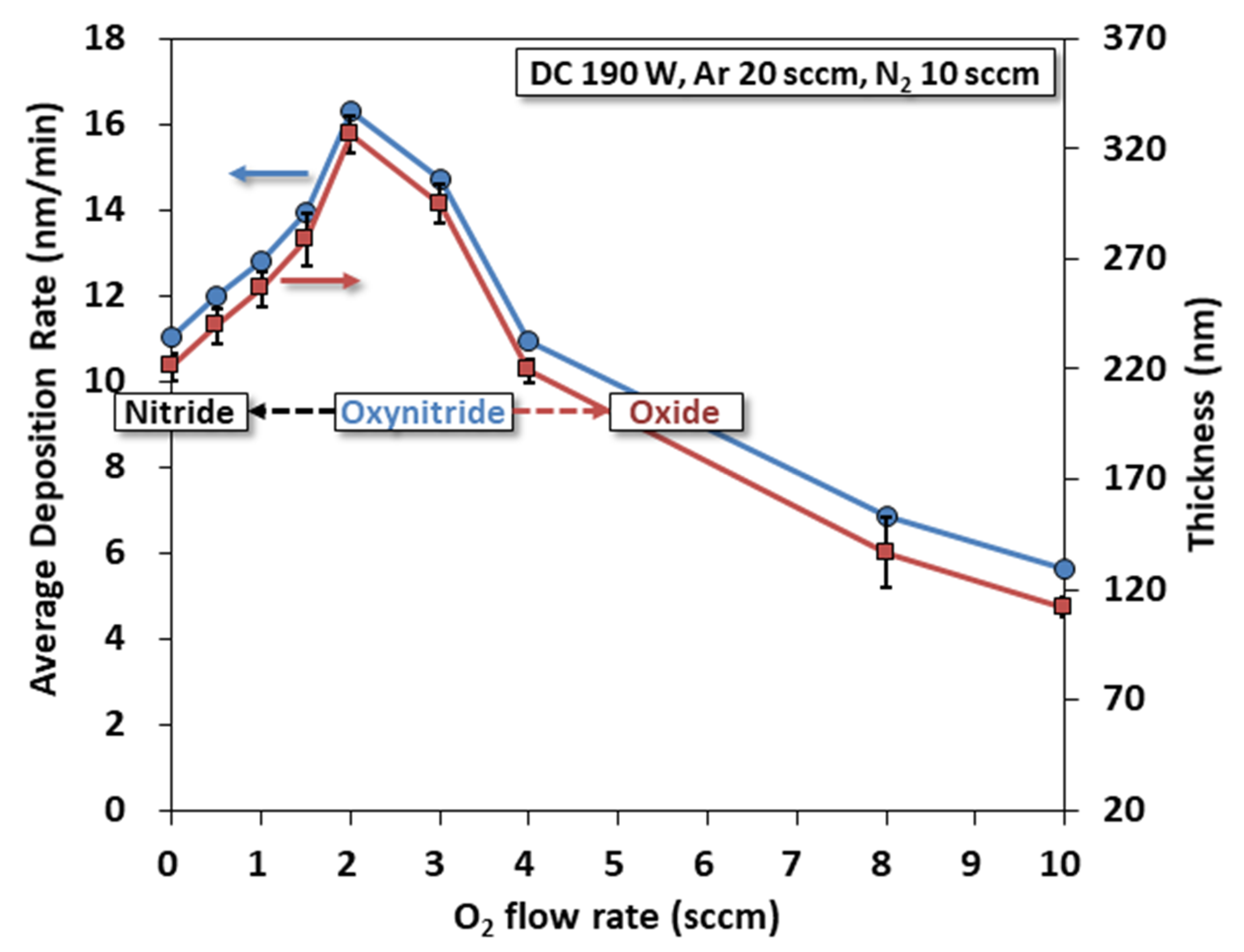
The average deposition rates and thickness of different films are shown in Figure 2 where the average deposition rate initially increases from 11.05 nm/min under 0 sccm oxygen to a maximum of 16.33 nm/min at 2 sccm oxygen. Then, the average deposition rate declines as the oxygen supply increases. It decreases to 10.95 nm/min at 4 sccm oxygen. The initial increase of deposition rate can be attributed to the formation of less dense oxynitrides or oxides, which rapidly thicken the deposited film. While the subsequent decrease is related to the poisoning of Ta target by oxygen, this makes the chamber plasma less conductive and thus lower deposition rates.
For all material characterizations in the following sections, we choose 200 nm as the target thickness to deposit films. The time for deposition then was estimated based on the average deposition rates in Figure 2.

3.2. XRD

The XRD pattern of annealed films is shown in Figure 3. For zero oxygen flow, sample after annealed, only TaN were found by Gaussian fit using Jade® 6.5. The peaks for TaN are (1,2,1), (0,0,2), (3,1,2), (5,0,1), and (2,4,2) (TaN, ICCD PDF 49-1283). The (1,2,1) crystal plane has the highest intensity with an estimated crystal size of 83.6 Å. For oxygen flow to increase to higher than 0.25 sccm, the oxynitride starts to form. Gaussian fit yields very complicated crystal structures with a large number of crystal planes (TaON, ICCD PDF 70-1193 and 71-0178) [37,38]. The signature peaks for tantalum oxynitrides are (−1,1,1), (1,1,1), and the tri-peaks are (0,0,2), (0,2,0), (2,0,0). As the oxygen flow increases to more than 1.5 sccm, tantalum oxynitrides are replaced by tantalum oxides due to the much higher chemical reactivity of oxygen than that of nitrogen. However, this kind of replacement is also aided by high-temperature annealing, which transforms the sample film into complex oxides indicated by the larger number of fitted crystal planes. The three major peaks of the tantalum oxides were found to be (0,0,1), (2,0,0), and (2,0,1) (Ta2O5, PDF 71-0639) for all sample films deposited under oxygen flow rate exceeding 1.5 sccm.
Oxynitrides cannot be totally separated from oxides or nitrides. For example, the tantalum oxynitrides (−1,1,1) and (2,0,0) crystal planes almost overlap those in the oxides (2,0,0) and (2,0,1), respectively. This is in line with the nature of oxynitrides, which are tri-elemental complex compounds of properties in between pure nitrides and oxides.
The estimated crystal sizes of selected crystal planes are listed in the Table A1 in Appendix A.
It is worth noting that the color of annealed films is changed according to different oxygen flow rates. For the lower O2 flow rate (~0.5 sccm), the film has a dark brown color. The color becomes more yellow and transparent when the O2 flow rate reaches ~1.0 sccm. When the O2 flow rate increases to 1.5 sccm, the film appears lighter green and even more transparent. As the O2 flow rate exceeds 2 sccm, the sample films all become transparent. This color change serves as an important indicator for the transformation of microstructure and associated optical properties, which are discussed below.

3.3. EDS

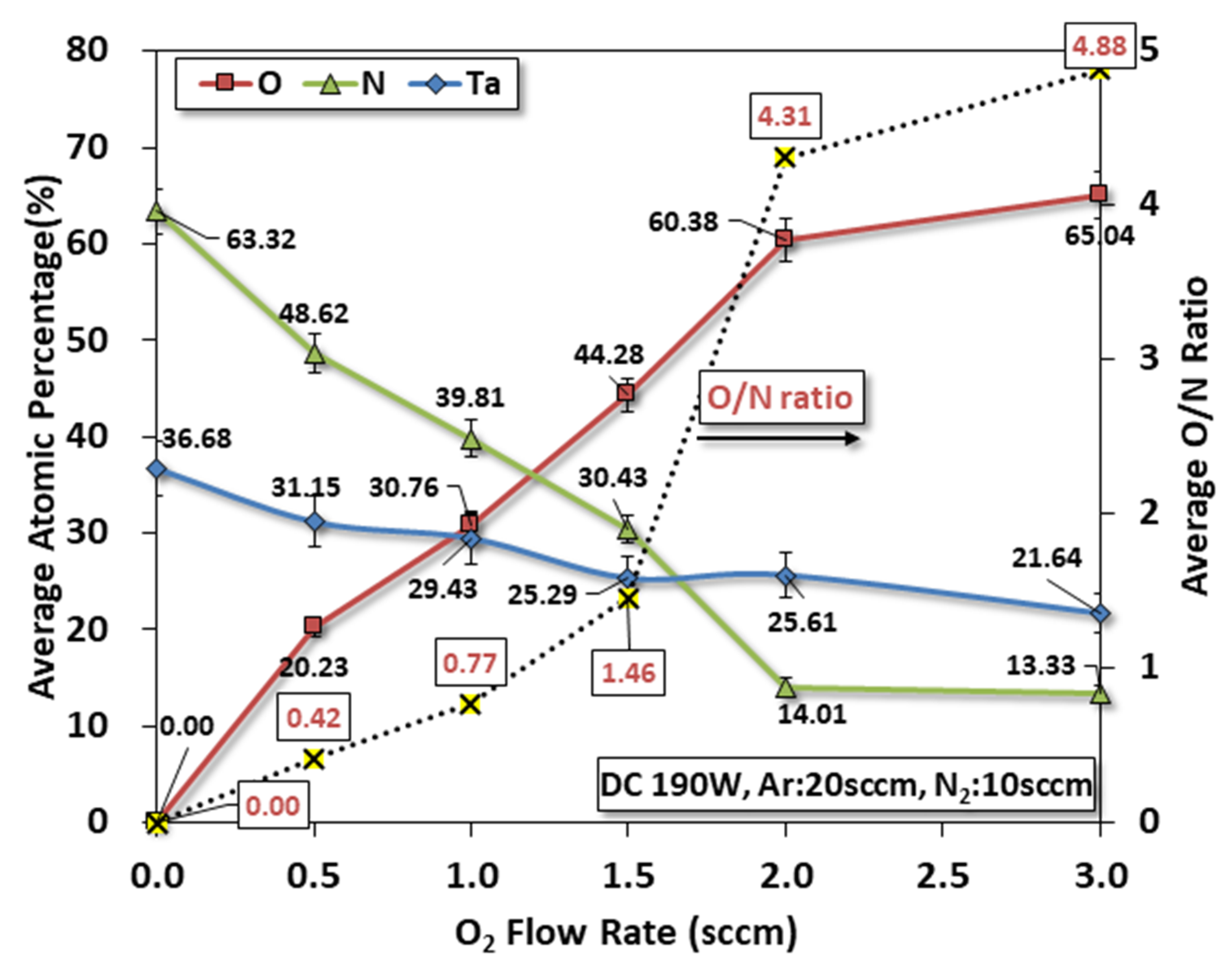
The elemental chemical compositions of annealed films in the selected surface areas under SEM are shown in Figure 4. SEM images accompanied with the EDS are provided in the supplementary section for readers’ reference. The most important observation from EDS is that the atomic percentage of O is increased (0–~65%) and N decreased (~63%–13%), correspondingly, by the increased oxygen supply. The amount of Ta also reduces (~37%–22%) but more marginally. This trend directly reflects the change of chemical compositions on the surface of films according to the change of oxygen supply.
Although it is commonly recognized that EDS is not an accurate measurement for the chemical composition, it is undeniable that EDS is a useful reference to show the changes of elemental compositions according to different oxygen flow rates. With further calculations on the O/N ratio from EDS, we found that this ratio increases significantly (0.77 at O2: 1.0 sccm–4.31 at O2: 2 sccm 1.45 at O2: 1.5 sccm–4.31 at O2: 2 sccm). A reference milestone is between 1.0 and 1.5 sccm, at which the O/N ratio exceeds unity. This also implies that tantalum oxides become a major phase for oxygen flow rate higher than 2 sccm. This change is close to results from the XRD pattern in which the oxides are clearly present in the film for oxygen flow rate exceeding 2 sccm. The substantial formation of tantalum oxides has a critical impact on the electrical and optical properties of the annealed films as discussed in the following sections.

3.4. Raman Spectra

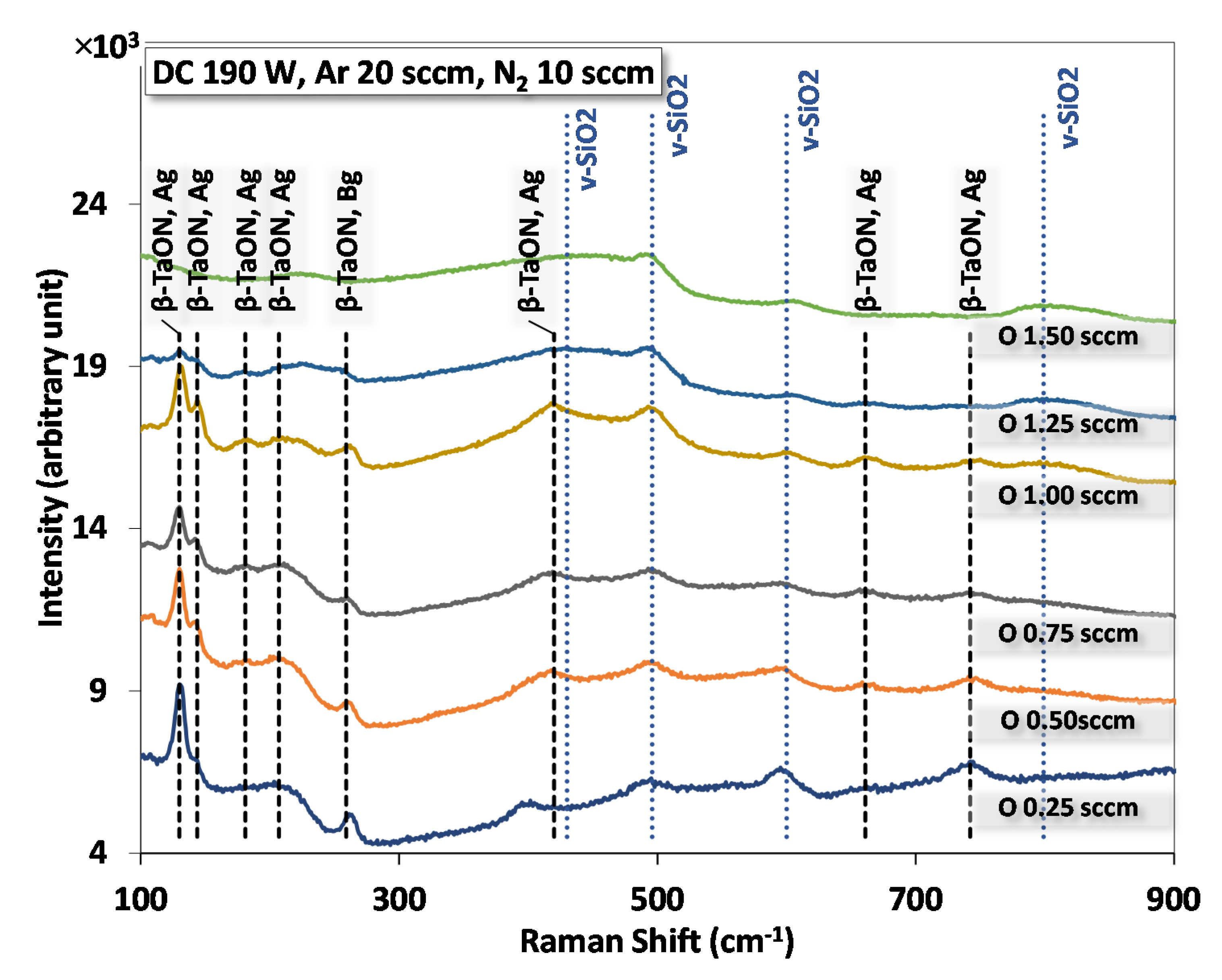
The Raman spectra of annealed films are shown in Figure 5 where peaks were numerically fitted by Gaussian functions. The vibrational modes of these peaks are listed in Table 2 with references. For annealed films deposited between 0.25 and 1.25 sccm, crystalline oxynitrides (β-TaON) can be determined. This is accordant with findings in XRD. For the sample film of 1.5-sccm oxygen flow rate or higher, the Raman shift peaks for Ta2O5 are difficult to be identified because they are gravely shadowed by the vibrational modes of the SiO2 substrate. Note that the film is about 200 nm thick while the substrate is around several mm. Disentangling peaks of Ta2O5 from those of SiO2 thus becomes infeasible in the current dataset.
Since the Raman spectroscopy determines the vibrational modes of chemical bonds based on the changes of molecular polarization by laser, the fitting result from Raman spectra accompanied with what was found in XRD and EDS provide evidence that (i) the oxynitride is β-TaON and (ii) oxynitrides are formed by oxygen flow from ~0.25 to ~1.5 sccm.

3.5. Electrical Resistivity

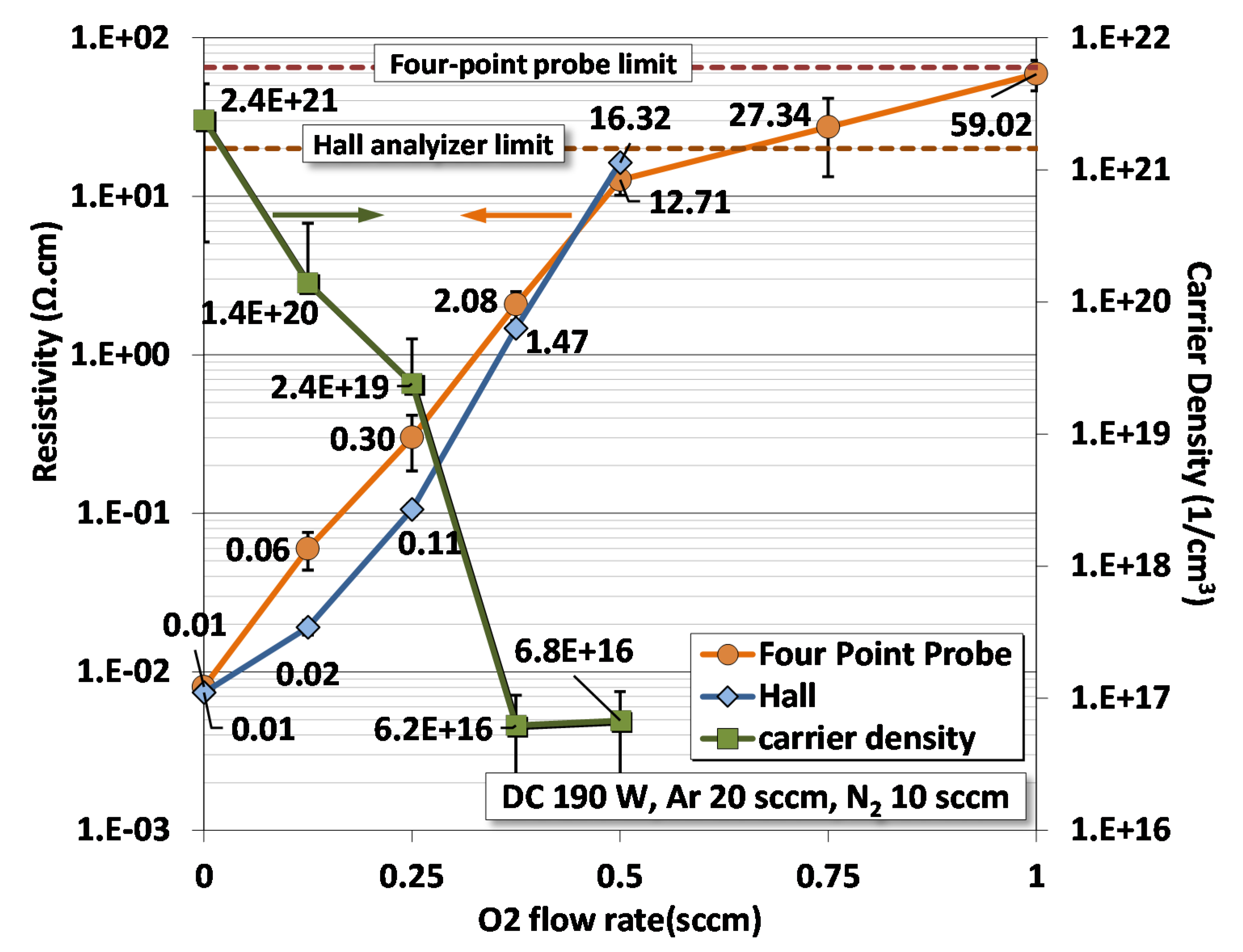
The electrical resistivity of annealed films is shown in Figure 6, where resistivities are measurable only for films deposited under oxygen supply up to 1.0 sccm. We note that the resistivity of deposited films measured by the four-point probe and the Hall effect analyzer are close to each other, which can be viewed as cross-validation of both experimental measures.
Note that there is a limit of the measurement for both devices because the thickness of films is about 200 nm, and the measurement takes on the resistance R via the relation R = ρ(l/A) to calculate resistivity ρ. If films are thicker (larger cross-sectional area A), then the limit of measurement can be higher.
The resistivity of deposited films is increased by more than three orders following the increase of oxygen flow rate from 0 to 1.0 sccm. This is due to the elevated oxygen content in films such that films change from tantalum nitrides (semi-conductive) to tantalum oxides (almost insulator) during deposition. Meanwhile, the lowered density of charge carriers for O2 higher than 0.25 sccm also raises the electrical resistivity of films significantly.
The electrical resistivity is a benchmark test for a transition of the semi-conductor to the insulator. For oxynitrides with desired photo-catalytical function, we preferred more semi-conductive materials with an appropriate width of bandgaps, which can support electron-hole separation without immediate recombination after optical irradiation. Based on this electrical measure, films deposited under 0.25 sccm or higher can be candidates for the photodegradation test.

3.6. UV-Vis-NIR Spectra

The UV-Vis-NIR spectra of various films deposited under different oxygen flow rates are shown in Figure 7, where optical transmittance, reflectance, and absorbance are presented over the range of 200–900 nm. There are several features found from these spectra:
  • For zero oxygen supply, the tantalum nitride film is almost opaque with very low transmittance. The optical reflectance is between 30 and 40%, and the absorbance reaches 60–90%.
  • As the oxygen supply increases from 0.5 sccm to 2 sccm, the transmittance also increases in the range of visible light. This result implies a gradually increased transparency of the films. Associated with this increase, there are “shoulders” in the variation of transmittance when light changes from the UV to visible light. Just like doping in semi-conductors, these shoulders indicate a possible existence of intra-bands in the films.
  • When the oxygen supply exceeds 2 sccm, the transmittance reaches above 80% in the range of visible light, while the absorbance reduces simultaneously to very low values. The switch between high and low transmittance and absorbance occurs around 300 nm. In other words, films become transparent in visible light. This also shows that these high-oxygen films are effective filters for UV light.
  • The color change of films is discussed in the section on XRD, and this change is in accordance with the variation of transmittance as shown in the inset of the photo.
  • Note that certain degrees of transparency with sufficient optical absorbance are a necessity for oxynitride films to achieve photocatalysis.

3.7. Optical Band Gap

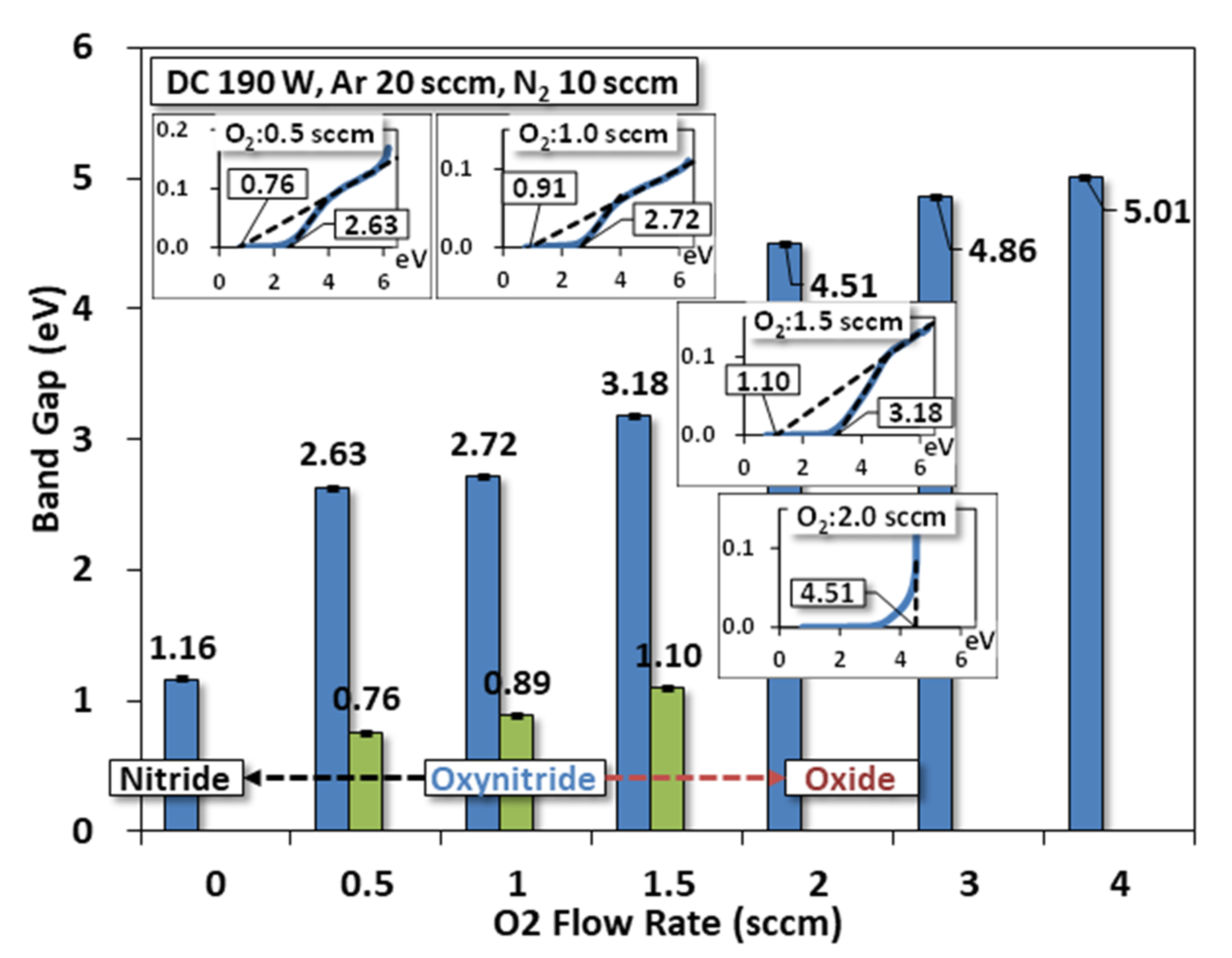
Using Equations (3) and (4) and the data from UV-VIS-NIR spectra, we can calculate the optical bandgaps of the annealed films. Figure 8 presents the estimated results for annealed films deposited under different oxygen flow rates. Four samples of calculation using the Tauc plot are also shown in the insets. As seen from the figure, when the O2 supply falls between 0.5 and 2.0 sccm, there exist two bands with a high energy level band between 2.6 and 3.2 eV, and a lower level one around 0.8–1.1 eV. The difference between these two bands is around 1.8–2.1 eV. Such a tandem combination provides an effective structure for the photocatalytic function as electrons can fully utilize the photon energy in the range of visible light to change their states from the valance band to the conduction band.
When O2 supply exceeds 2.0 sccm, the energy level of both bands is simply too high for electrons to reach even if UV energy is provided. This also explains why films become transparent at a higher O2 flow rate as mentioned earlier.
Based on results from XRD, EDS, Raman, electrical resistivity, UV-Vis-NIR spectra, and estimated optical band gaps, we could comfortably select films deposited under 0.5, 1.0, and 1.5 sccm O2 flow for the photodegradation test in the next section because these films are almost certainly oxynitrides.

3.8. Photodegradation Test

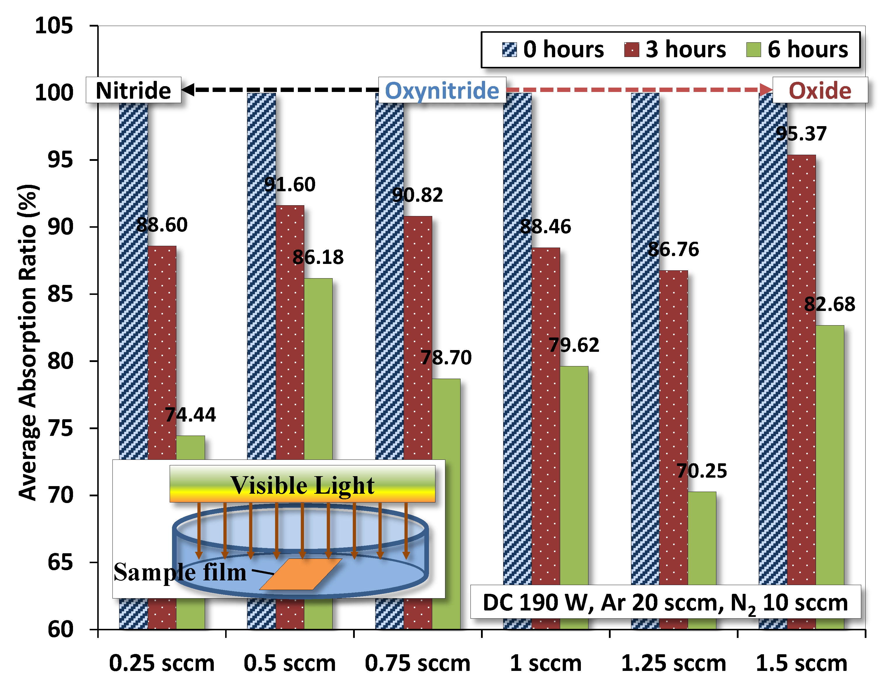
The results of photodegradation against the methyl orange in DI water are shown in Figure 9. We present results using the ratio of absorption as defined in Equation (6) for different exposure times up to 6 h. In all samples, the methyl orange was decomposed as time elapsed. Nevertheless, annealed films deposited between 0.25 and 1.25 sccm have higher efficiency on the degradation of methyl orange. This may be attributed to the sufficient quantity of oxynitrides in the film by the higher O2 supply. Since the methyl orange is quite stable even under long-term exposure to solar light, this test demonstrates the feasibility of photodegradation by tantalum oxynitrides under mildly visible light irradiation.

4. Discussion

4.1. Optimal Choice for Photocatalysis

The purpose of various material characterizations in this study is to provide us an optimal window of deposition parameters (oxygen flow rate) for the fabrication of tantalum oxynitride films with appropriate microstructures, enabling photocatalytic function. The following is a summary of different experimental results for obtaining a photocatalytic tantalum oxynitrides film:
  • Crystalline phases: Both XRD and Raman detects the formation in films for O2 flow between ~0.25 and ~1.25 sccm;
  • Limited oxygen: EDS roughly indicates that the content in films can be maintained for O2 flow less than 1.5 sccm;
  • Semi-conductivity: Four-point probe and Hall effect analyzer predict finite electrical resistivity for O2 flow between ~0.25 and ~1.0 sccm;
  • Semi-transparent with sufficient optical absorption: UV-Vis-NIR observes such for O2 flow between ~0.5 –~1.5 sccm;
  • Intra-bands: Tauc plot estimates the presence of dual optical bandgaps for O2 flow between ~0.5 and ~1.5 sccm;
  • Efficiency: Photodegradation of methyl orange estimates higher efficiency for films deposited by ~0.25 and 1.25 sccm O2 flow.
Combining results from all the above assessments, we suggest that annealed tantalum oxynitride films deposited under ~0.25–1.5 sccm O2 supply should be capable of photocatalysis in our current setups for magnetron sputtering.

4.2. Electrical and Optical Characters Comparison

We briefly compare our results with few previous studies with a focus on the electrical resistivity and optical bandgaps as these two measurements are straight without further interpretations. A quantitative comparison is nearly impossible due to various factors such as deposition conditions, film microstructures, and hardware controls.
For electrical resistivity, our crystalline tantalum oxynitride samples present values of 1 × 10⁻²–5.9 × 101 Ω cm. The amorphous tantalum oxynitride (Ta-O-N) films are ~4 × 10⁻¹ Ω cm in [38]; Ta–N–O thin films by reactive co-sputtering under partial pressure ratio PO/(PO+PN) = 0.22–0.79 is between 2.88 × 10⁻⁴ and 1.15 × 10⁴ Ω cm in [42]; TaON epitaxial thin films is 1 × 10⁻² Ω cm in [43]; tantalum oxynitride thin films by r.f. reactive magnetron sputtering is 4 × 10⁻⁴–1 × 10⁻³ Ω cm in [44]; TaON films deposited at 2500 W and annealed at 500 °C in N2 exhibited resistivity 4.6 × 10⁻⁴ Ω cm [45].
As for the optical bandgap, our films exhibit dual bands with the high band resides between 2.63–3.18 eV. The gap between the two bands is within 1.87–2.08 eV. The amorphous tantalum oxynitride (Ta-O-N) films in [38] have a bandgap width of 2.45 eV; TaON epitaxial thin films in [43] were found to be 2.37 eV. TaOxNy thin films under Ar 70 sccm, 85%N2 + 15%O2 gas mixture flow 2.5–30 sccm (partial pressure 0.02–0.24 Pa) have bandgaps 2.265–1.436 eV and valance band at 2.61–2.19 eV [46]. In fact, most tantalum oxynitrides have bandgaps between 1.9 and 2.5 eV [1,3,47].
Lastly, a tentative, non-quantitative comparison for the photodegradation of methylene orange between our results and a recent study in [46] can provide a clue on the efficiency of TaON films under visible light. Our results indicate that TaON by 0.5–1.5 sccm O2 degrades 14 to 29.5% of methylene orange, while it is reported around 10% for TaON under partial pressure 0.02–0.24 Pa of 85%N2 + 15%O2 gas mixture. Reference [46] provides abundant results from various characterizations and tests for sputtered tantalum oxynitride films.

5. Conclusions

Tantalum oxynitride films were deposited by sputtering under a fixed nitrogen flow (10 sccm) but variable oxygen flow (0–4 sccm). Post rapid thermal annealing process was conducted at 800 °C for 5 min to transform the deposited film from amorphous into crystalline. The films were characterized by XRD and Raman for their crystal structures; SEM for surface morphologies, EDS for surface chemical compositions, Four-point probe and Hall effect analyzer for electrical resistivity, and UV-VIS-NIR spectroscopy for optical transmittance, reflectance, and absorbance. Tauc-plot and Beer-Lambert law were used to estimate the optical band gaps of films from the UV-VIS-NIR spectra. Results indicate that under low oxygen supply (0.25–1.0 sccm), the deposited films are nitride-rich, lower electrically resistive, brown in color, and have low transparency. As the oxygen flow rate increased to 1.0–2.0 sccm, the films changed their colors from brown to yellow and light green with higher transparency and electrical resistivity. These semi-transparent films are oxynitrides with double optical bands at the energy level of visible light. When the oxygen flow rate exceeds 2.0 sccm, films turn into totally transparent oxides. These oxides have wide optical band gaps (>3.4 eV) only utilizable by the photons of UV light.
Based upon the results of XRD, Raman, EDS, electrical resistivity, and UV-VIS-NIR, we selected the annealed films deposited under 0.5–1.5 sccm O2 supply for the photodegradation test against methyl orange in DI water. Results from the degradation test indicate that annealed films deposited between 0.25 and 1.5 sccm O2 flow can degrade 14% or more methyl orange solution when continuously exposed to simulated solar light after six hours.

Author Contributions

Individual contributions for this study are specified in the following: Conceptualization, C.L. and J.-H.H.; methodology, C.L. and J.-H.H.; software, Y.R.C.; validation, C.L., J.-H.H. and Y.R.C.; formal analysis, C.L. and Y.R.C.; investigation, C.L., J.-H.H. and Y.R.C.; resources, C.L. and J.-H.H.; data curation, Y.R.C.; writing—original draft preparation, C.L.; writing—review and editing, C.L. and J.-H.H.; visualization, C.L. and Y.R.C.; supervision, C.L. and J.-H.H.; project administration, C.L.; funding acquisition, C.L. and J.-H.H. All authors have read and agreed to the published version of the manuscript.

Conflicts of Interest

The authors declare no conflict of interest.

Appendix A. Estimated Crystal Size

Table A1 gives estimated crystal sizes of major peaks in XRD using Sherrer’s formula. The selection is based on the intensity of peaks, and for brevity only five or six are tabulated for each oxygen flow rate.
Table A1. Estimated crystal size for major peaks in XRD.
O2 Flow Rate (sccm)2-ThetaEst. Crystal Size (Å)(h,k,l)
0 sccm, TaN36.2883.60(1,2,1)
42.0888.85(0,0,2)
27.9970.58(2,0,0)
22.9994.82(1,0,1)
60.9867.84(3,1,2)
0.25 sccm, TaON31.82173.18unknown
36.76147.64(2,0,0)
29.1496.23(−1,1,1)
53.08167.86(−2,2,1)
28.44116.25(1,11,0)
0.5 sccm, TaON29.19151.18(−1,1,1)
32.79132.71(1,1,1)
31.72155.24unknown
36.74169.45(2,0,0)
52.24169.50(−1,2,2)
35.2687.84(0,0,2)
0.75 sccm, TaON29.18137.28(−1,1,1)
32.81144.53(1,1,1)
36.76143.84(2,0,0)
35.2777.98(0,0,2)
52.20171.11(2,2,0)
1.0 sccm, TaON29.21148.72(−1,1,1)
32.83156.26(1,1,1)
36.79185.22(2,0,0)
35.80186.35(0,2,0)
52.24205.29(−1,2,2)
1.25 sccm, TaON29.0190.97(2,1,1)
36.78151.39(2,0,0) *
32.87150.05(1,1,1)
28.56126.51(−1,1,1) *
52.28184.36(−1,2,2)
1.5 sccm, Ta2O536.92161.37(2,0,0)
22.94166.45(0,0,1)
55.75101.32(1,11,2)
50.4295.13(3,3,1)
28.48157.92(−1,1,1)
46.74189.37(3,7,0)
2.0 sccm, Ta2O528.59181.37(−1,1,1)
36.98181.71(2,0,0)
22.99199.19(0,0,1)
55.8499.90(1,11,2)
50.6090.96(3,3,1)
46.86202.29(3,7,0)
4.0 sccm, Ta2O523.01227.09(0,0,1)
28.65192.92(−1,1,1)
37.03214.82(2,0,0)
55.83121.33(1,11,2)
46.91240.55(3,7,0)
50.68115.81(3,3,1)
* Peaks should belong to Ta2O5.

Appendix B. SEM

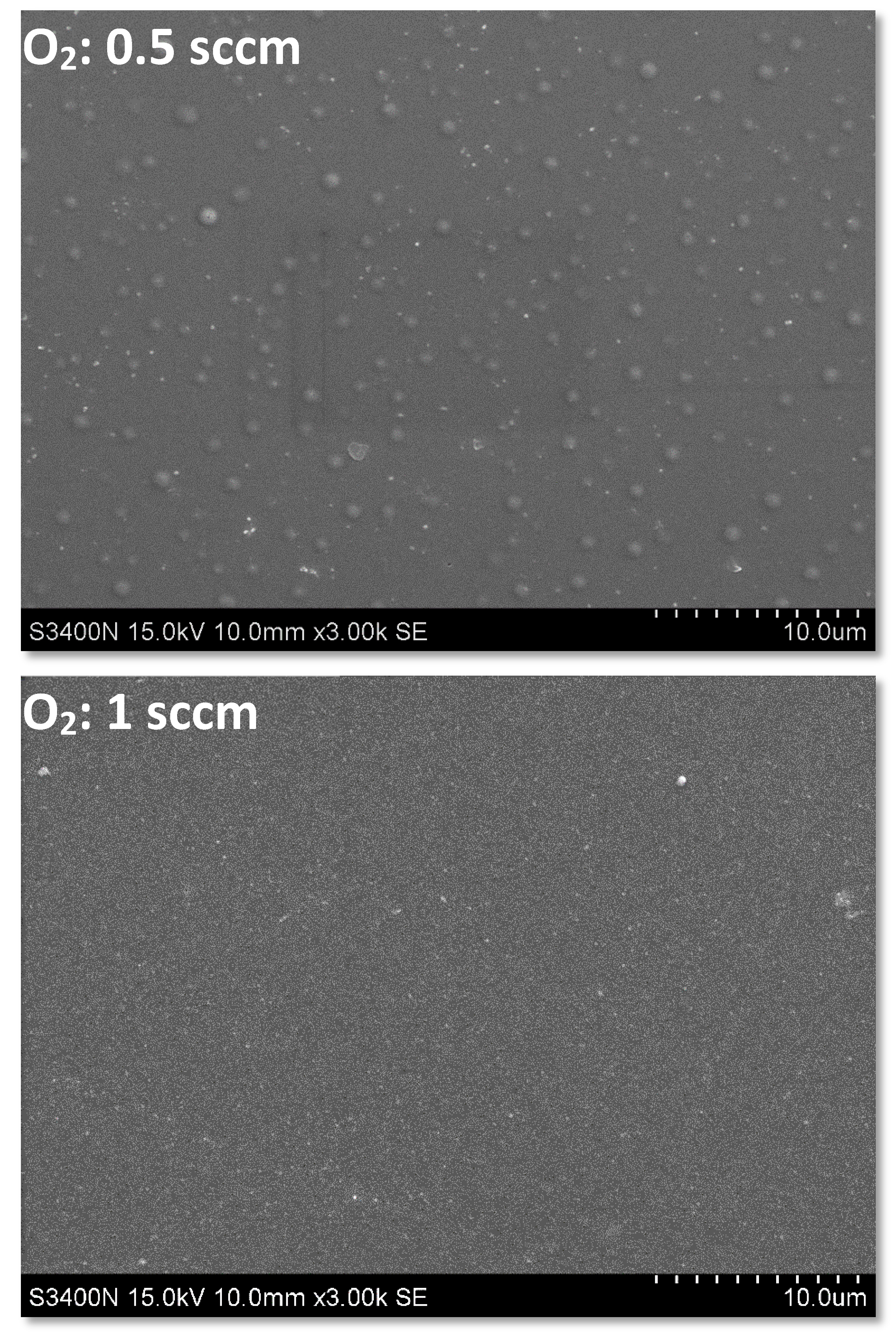
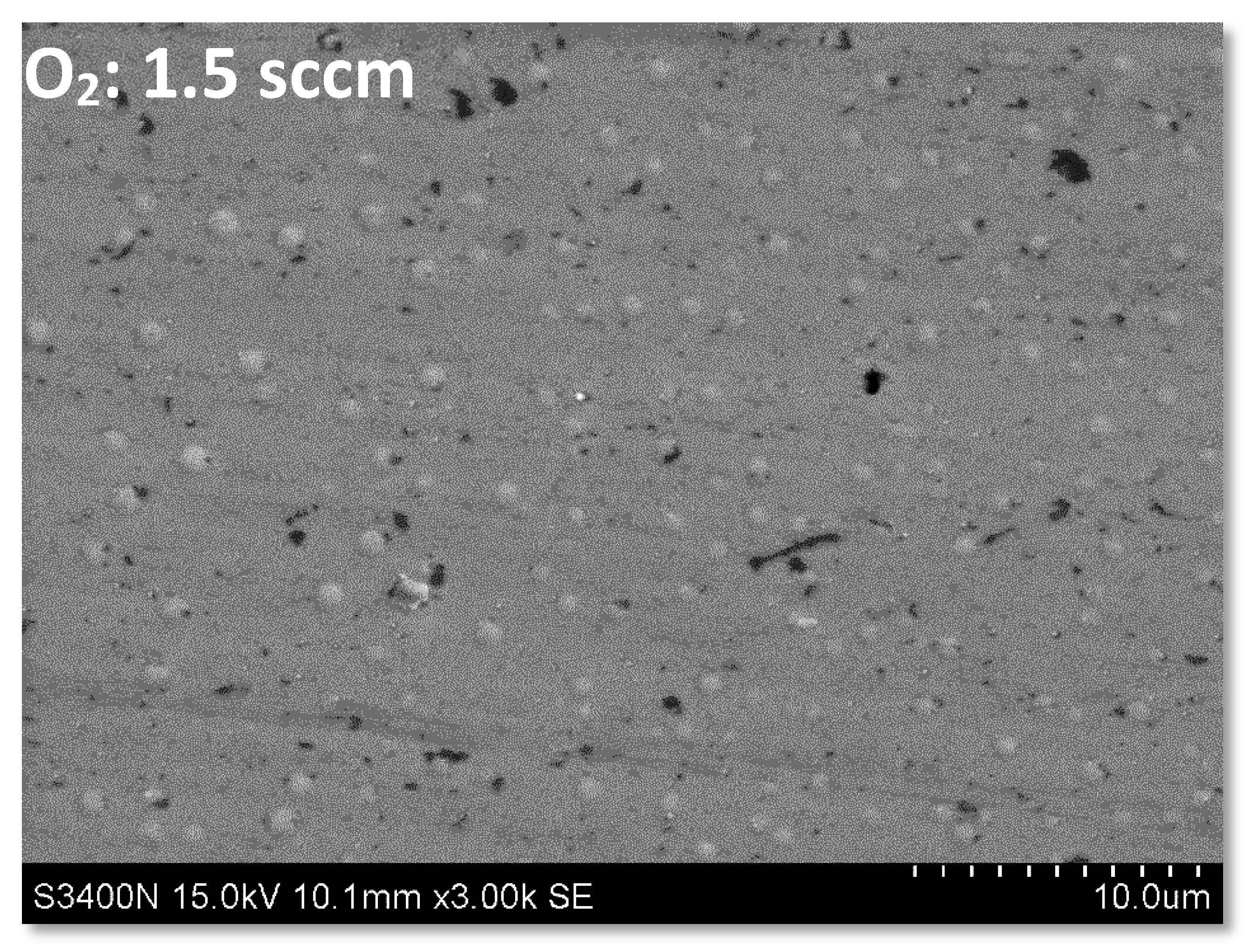
The surface morphology of selected annealed films by SEM is shown in Figure A1. Three sample films deposited under O2 flow rates of 0.5, 1.0, and 1.5 sccm were chosen to demonstrate the transition from the phase of nitride-rich to oxide-rich. Among the three samples, the surface of films deposited under 1.0 sccm oxygen supply appears to be the smoothest one. This could indicate that the condition of 1.0 sccm oxygen supply provides an optimal balance between the nitride and the oxide to result in more coherent microstructures. It is also noticed that there are many spherical precipitates at 0.5 and 1.5 sccm O2 flow that could be Ta metallic phases, but their dimensions are too small to be distinguished by our EDS system.
Figure A1. Selected SEM images of annealed films under different oxygen flow rates.
Photonics 08 00053 g0a1aPhotonics 08 00053 g0a1b

References

  1. Ahmed, M.; Guo, X. A review of metal oxynitrides for photocatalysis. Inorg. Chem. Front. 2016, 3, 578–590. [Google Scholar] [CrossRef]
  2. Cubillos, G.I.; Bethencourt, M.; Olaya, J.J. Corrosion resistance of zirconium oxynitride coatings deposited via DC unbal-anced magnetron sputtering and spray pyrolysis-nitriding. Appl. Surf. Sci. 2015, 327, 288–295. [Google Scholar] [CrossRef]
  3. Maeda, K.; Kazunari, D. Oxynitride materials for solar water splitting. MRS Bull. 2011, 36, 25–31. [Google Scholar] [CrossRef]
  4. Cao, G.Z.; Metselaar, R. α’-Sialon Ceramics: A Review. Chem. Mater. 1991, 3, 242–252. [Google Scholar] [CrossRef] [Green Version]
  5. Luo, Z.; Qu, G.; Zhang, Y.; Cui, L.; Lu, A. Transparent oxynitride glasses: Synthesis, microstructure, optical transmittance and ballistic resistance. J. Non-Cryst. Solids 2013, 378, 45–49. [Google Scholar] [CrossRef]
  6. Lei, P.; Guo, S.; Zhu, J.; Dai, B.; Liu, G.; Wang, Y.; Han, J. Enhanced mechanical properties of HfO2film by nitrogen doping. Surf. Eng. 2016, 32, 585–588. [Google Scholar] [CrossRef]
  7. Gibson, J.S.K.-L.; Rezaei, S.; Rueß, H.; Hans, M.; Music, D.; Wulfinghoff, S.; Schneider, J.M.; Reese, S.; Korte-Kerzel, S. From quantum to continuum mechanics: Studying the fracture toughness of transition metal nitrides and oxynitrides. Mater. Res. Lett. 2018, 6, 142–151. [Google Scholar] [CrossRef] [Green Version]
  8. Ebbinghaus, S.G.; Abicht, H.-P.; Dronskowski, R.; Müller, T.; Reller, A.; Weidenkaff, A. Perovskite-related oxynitrides—Recent developments in synthesis, characterization and investigations of physical properties. Prog. Solid State Chem. 2009, 37, 173–205. [Google Scholar] [CrossRef] [Green Version]
  9. Iqbal, N.; Khan, I.; Yamani, Z.H.; Qurashi, A. Sonochemical Assisted Solvothermal Synthesis of Gallium Oxynitride Nanosheets and their Solar-Driven Photoelectrochemical Water-Splitting Applications. Sci. Rep. 2016, 6, 32319. [Google Scholar] [CrossRef] [Green Version]
  10. Shaheen, B.S.; Hafez, A.M.; Murali, B.; Kirmani, A.R.; Amassian, A.; Mohammed, O.F.; Allam, N.K. 10-fold enhancement in light-driven water splitting using niobium oxynitride microcone array films. Sol. Energy Mater. Sol. Cells 2016, 151, 149–153. [Google Scholar] [CrossRef]
  11. Black, A.P.; Suzuki, H.; Higashi, M.; Frontera, C.; Ritter, C.; De, C.; Sundaresan, A.; Abe, R.; Fuertes, A. New rare earth hafnium oxynitride perovskites with photocatalytic activity in water oxidation and reduction. Chem. Commun. 2018, 54, 1525–1528. [Google Scholar] [CrossRef] [Green Version]
  12. Yang, M.-C.; Yang, T.-S.; Wong, M.-S. Nitrogen-doped titanium oxide films as visible light photocatalyst by vapor deposition. Thin Solid Films 2004, 469, 1–5. [Google Scholar] [CrossRef]
  13. Kitano, M.; Matsuoka, M.; Ueshima, M.; Anpo, M. Recent developments in titanium oxide-based photocatalysts. Appl. Catal. A Gen. 2007, 325, 1–14. [Google Scholar] [CrossRef]
  14. Lai, K.; Huang, J.Y.; Zhang, H.F.; Subramaniam, V.P.; Tang, Y.X.; Gong, D.G.; Sundar, L.; Sun, L.; Chen, Z.; Lin, C.J. Nitrogen-doped TiO2 nanotube array films with enhanced photocatalytic activity under various light sources. J. Hazard Mater. 2010, 184, 855–863. [Google Scholar] [CrossRef]
  15. Triantis, T.M.; Fotiou, T.; Kaloudis, T.; Kontos, A.G.; Falaras, P.; Dionysiou, D.D.; Pelaez, M.; Hiskia, A. Photocatalytic deg-radation and mineralization of microcystin-LR under UV-A, solar and visible light using nanostructured nitrogen doped TiO2. J. Hazard Mater. 2012, 211, 196–202. [Google Scholar] [CrossRef]
  16. Fuertes, A. Synthetic approaches in oxynitride chemistry. Prog. Solid State Chem. 2018, 51, 63–70. [Google Scholar] [CrossRef]
  17. Watanabe, T.; Tajima, K.; Li, J.; Matsushita, N.; Yoshimura, M. Low-temperature Ammonothermal Synthesis of LaTaON2. Chem. Lett. 2011, 40, 1101–1102. [Google Scholar] [CrossRef]
  18. Higashi, M.; Domen, K.; Abe, R. Fabrication of an Efficient BaTaO2N Photoanode Harvesting a Wide Range of Visible Light for Water Splitting. J. Am. Chem. Soc. 2013, 135, 10238–10241. [Google Scholar] [CrossRef] [PubMed]
  19. Kim, Y.-I.; Si, W.; Woodward, P.M.; Sutter, E.; Park, S.; Vogt, T. Epitaxial Thin-Film Deposition and Dielectric Properties of the Perovskite Oxynitride BaTaO2N. Chem. Mater. 2007, 19, 618–623. [Google Scholar] [CrossRef]
  20. Khodaei, M.; Yaghobizadeh, O.; Alhosseini, S.H.N.; Esmaeeli, S.; Mousavi, S.R. The effect of oxide, carbide, nitride and boride additives on properties of pressureless sintered SiC: A review. J. Eur. Ceram. Soc. 2019, 39, 2215–2231. [Google Scholar] [CrossRef]
  21. Chen, H.-Y.; Lu, F.-H. Oxidation behavior of titanium nitride films. J. Vac. Sci. Technol. A 2005, 23, 1006–1009. [Google Scholar] [CrossRef] [Green Version]
  22. Wright, J.S.; Lim, W.; Norton, D.P.; Pearton, S.J.; Ren, F.; Johnson, J.L.; Ural, A. Nitride and oxide semiconductor nanostruc-tured hydrogen gas sensors. Semicond. Sci. Technol. 2010, 25, 024002. [Google Scholar] [CrossRef]
  23. Ghosh, S.; Jeong, S.M.; Polaki, S.R. A review on metal nitrides/oxynitrides as an emerging supercapacitor electrode beyond oxide. Korean J. Chem. Eng. 2018, 35, 1389–1408. [Google Scholar] [CrossRef]
  24. Bahari, A.; Morgen, P.; Pedersen, K.; Li, Z.S. Growth of a stacked silicon nitride/silicon oxide dielectric on Si (100). J. Vac. Sci. Technol. B Microelectron. Nanometer Struct. 2006, 24, 2119. [Google Scholar] [CrossRef]
  25. Leitao, A.B.V.; Lima, C.L.; Viana, B.C.; Neto, B.; Costa, J.A.P.; Costa, T.H.C.; De Souza, I.A.; Naeem, M.; Sousa, R.R.M. Novel synthesis of molybdenum nitride/oxide on AISI-316 steel assisted with active screen plasma treatment. Mater. Res. Express 2019, 6, 116501. [Google Scholar] [CrossRef]
  26. Dietl, T. A ten-year perspective on dilute magnetic semiconductors and oxides. Nat. Mater. 2010, 9, 965–974. [Google Scholar] [CrossRef] [Green Version]
  27. Gerstenberg, D.; Calbick, C.J. Effects of nitrogen, methane, and oxygen on structure and electrical properties of thin tantalum films. J. Appl. Phys. 1964, 35, 402–407. [Google Scholar] [CrossRef]
  28. Cardonne, S.; Kumar, P.; Michaluk, C.; Schwartz, H. Tantalum and its alloys. Int. J. Refract. Met. Hard Mater. 1995, 13, 187–194. [Google Scholar] [CrossRef]
  29. Tauc, J.; Grigorovici, R.; Vancu, A. Optical Properties and Electronic Structure of Amorphous Germanium. Phys. Status Solidi B 1966, 15, 627–637. [Google Scholar] [CrossRef]
  30. Tauc, J. Optical properties and electronic structure of amorphous Ge and Si. Mater. Res. Bull. 1968, 3, 37–46. [Google Scholar] [CrossRef]
  31. Beer, A. Bestimmung der absorption des rothen lichts in farbigen flussigkeiten. Ann. Phys. 1852, 162, 78–88. [Google Scholar] [CrossRef] [Green Version]
  32. Rahman, M.; Krishna, K.; Soga, T.; Jimbo, T.; Umeno, M. Optical properties and X-ray photoelectron spectroscopic study of pure and Pb-doped TiO2 thin films. J. Phys. Chem. Solids 1999, 60, 201–210. [Google Scholar] [CrossRef]
  33. Tang, H.; Prasad, K.; Sanjinès, R.; Schmid, P.E.; Lévy, F. Electrical and optical properties of TiO2anatase thin films. J. Appl. Phys. 1994, 75, 2042–2047. [Google Scholar] [CrossRef]
  34. Sharma, P.; Vashistha, M.; Jain, I.P. Optical properties of Ge20Se80-xBix thin films. J. Optoelectron. Adv. Mater. 2005, 7, 2647–2654. [Google Scholar]
  35. Li, C.; Hsieh, J.H.; Hung, M.T.; Huang, B.Q. The deposition and microstructure of amorphous tungsten oxide films by sputtering. Vacuum 2015, 118, 125–132. [Google Scholar] [CrossRef]
  36. Li, C.; Hsieh, J.H.; Su, T.Y.; Wu, P.L. Experimental Study on Property and Electrochromic Function of Stacked WO3/Ta2O5/NiO Films by Sputtering. Thin Solid Films 2018, 66, 373–379. [Google Scholar] [CrossRef]
  37. Salamon, K.; Mičetić, M.; Sancho-Parramon, J.; Radović, I.B.; Siketić, Z.; Šarić, I.; Petravić, M.; Bernstorff, S. β-TaON thin films: Production by reactive magnetron sputtering and the question of non-stoichiometry. J. Phys. D Appl. Phys. 2019, 52, 305304. [Google Scholar] [CrossRef]
  38. Čapek, J.; Batková, Š.; Haviar, S.; Houška, J.; Čerstvý, R.; Zeman, P. Effect of annealing on structure and properties of Ta–O–N films prepared by high power impulse magnetron sputtering. Ceram. Int. 2019, 45, 9454–9461. [Google Scholar] [CrossRef]
  39. Nurlaela, E.; Harb, M.; Del Gobbo, S.; Vashishta, M.; Takanabe, K. Combined experimental and theoretical assessments of the lattice dynamics and optoelectronics of TaON and Ta3N5. J. Solid State Chem. 2015, 229, 219–227. [Google Scholar] [CrossRef] [Green Version]
  40. Li, P.; Fan, W.; Li, Y.; Sun, H.; Cheng, X.; Zhao, X.; Jiang, M. First-Principles Study of the Electronic, Optical Properties and Lattice Dynamics of Tantalum Oxynitride. Inorg. Chem. 2010, 49, 6917–6924. [Google Scholar] [CrossRef] [PubMed]
  41. Ivanda, M.; Clasen, R.; Hornfeck, M.; Kiefer, W. Raman spectroscopy on SiO2 glasses sintered from nanosized particles. J. Non-Cryst. Solids 2003, 322, 46–52. [Google Scholar] [CrossRef]
  42. Chung, C.; Chen, T.; Chang, N. Effect of reactive gases flow ratios on the microstructure and electrical resistivity of Ta–N–O thin films by reactive co-sputtering. Thin Solid Films 2011, 519, 5099–5102. [Google Scholar] [CrossRef]
  43. Suzuki, A.; Hirose, Y.; Oka, D.; Nakao, S.; Fukumura, T.; Ishii, S.; Sasa, K.; Matsuzaki, H.; Hasegawa, T. High-Mobility Electron Conduction in Oxynitride: Anatase TaON. Chem. Mater. 2014, 26, 976–981. [Google Scholar] [CrossRef]
  44. Ayerdi, I.; Castaño, E.; García-Alonso, A.; Gracia, F.J. Characterization of tantalum oxynitride thin films as high-temperature strain gauges. Sens. Actuator A Phys. 1995, 46, 218–221. [Google Scholar] [CrossRef]
  45. Lee, P.-Y.; Lin, C.-X.; Lee, Y.-C. Microstructure and electrical property of tantalum oxynitride thin films prepared using high-power impulse reactive magnetron sputtering. Jpn. J. Appl. Phys. 2020, 59, 116502. [Google Scholar] [CrossRef]
  46. Cristea, D.; Cunha, L.; Gabor, C.; Ghiuta, I.; Croitoru, C.; Marin, A.; Velicu, L.; Besleaga, A.; Vasile, B. Tantalum Oxynitride Thin Films: Assessment of the Photocatalytic Efficiency and Antimicrobial Capacity. Nanomater 2019, 9, 476. [Google Scholar] [CrossRef] [Green Version]
  47. Zhen, C.; Chen, R.; Wang, L.; Liu, G.; Cheng, H.-M. Tantalum (oxy)nitride based photoanodes for solar driven water oxidation. J. Mater. Chem. A 2016, 4, 2783–2800. [Google Scholar] [CrossRef] [Green Version]
Figure 1. Experimental procedure and plan.
Photonics 08 00053 g001
Figure 2. The average deposition rate and thickness of deposited films.
Photonics 08 00053 g002
Figure 3. XRD patterns of annealed films deposited under different oxygen flow rates.
Photonics 08 00053 g003
Figure 4. Estimated elemental compositions from EDS of annealed films under different oxygen flow rates.
Photonics 08 00053 g004
Figure 5. Raman spectra of annealed films under different oxygen flow rates.
Photonics 08 00053 g005
Figure 6. Electrical resistivity and carrier density of annealed films under different oxygen flow rates.
Photonics 08 00053 g006
Figure 7. UV-Visible-NIR absorbance spectra of annealed films under different oxygen flow rates.
Photonics 08 00053 g007aPhotonics 08 00053 g007b
Figure 8. Estimated optical band gaps in annealed films based on the UV-Visible-NIR spectra using the Tauc plot.
Photonics 08 00053 g008
Figure 9. Photodegradation of methyl orange by various annealed oxynitride films under visible light.
Photonics 08 00053 g009
Table 1. Parameters for PVD and rapid thermal annealing process.
Sputtering
ParameterSet Value
Target power (W)DC 190
Target compositionTa (99.9999 wt.%)
Background pressure (Pa)6.4 × 10⁻⁴
Working pressure (Pa)0.87–0.93 approx.
Substrate temperature (°C)Room temperature
Target-substrate distance (cm)10
Substrate bias (V)0
O2 flow rate (sccm)0, 0.13, 0.25, 0.38, 0.5, 0.75, 1, 1.5, 2, 4
Ar flow rate (sccm)20
N2 flow rate (sccm)10
Annealing
ParameterSet Value
Temperature (°C)800
Time (min)5
Ar flow rate (sccm)5000
Table 2. Possible peaks in Raman spectra for tantalum oxynitride and silicon oxides (substrate).
Wavenumber (cm−1)ModeDescriptionReference
131.5Agβ-TaON vibration[39,40,41]
143.8Agβ-TaON vibration[39,40,41]
183.8Agβ-TaON vibration[39]
207.0Agβ-TaON vibration[40,41]
257.6Bgβ-TaON vibration[39,40]
419.7Agβ-TaON vibration[39]
350~450 v-SiO2 Bond bending[41]
495 v-SiO2 D1[41]
606 v-SiO2 D2[41]
652.9Agβ-TaON vibrations[39]
735.6Bgβ-TaON vibrations[39,40]
780~850 v-SiO2 Tetrahedral[41]
Publisher’s Note: MDPI stays neutral with regard to jurisdictional claims in published maps and institutional affiliations.