Article

Investigation of Threshold Carrier Densities in the Optically Pumped Amplified Spontaneous Emission of Formamidinium Lead Bromide Perovskite Using Different Excitation Wavelengths

by
Saif M. H. Qaid
1,2,*,
Hamid M. Ghaithan
1,
Khulod K. AlHarbi
1,
Abrar F. Bin Ajaj
1,
Bandar Ali Al-Asbahi
1,3 and
Abdullah S. Aldwayyan
1,4,5,*
1
Physics and Astronomy Department, College of Science, King Saud University, Riyadh 11451, Saudi Arabia
2
Department of Physics, Faculty of Science, Ibb University, Ibb 70270, Yemen
3
Department of Physics, Faculty of Science, Sana’a University, Sana’a 12544, Yemen
4
King Abdullah Institute for Nanotechnology, King Saud University, Riyadh 11451, Saudi Arabia
5
K.A.CARE Energy Research and Innovation Center, King Saud University, Riyadh 11451, Saudi Arabia
*
Authors to whom correspondence should be addressed.
Photonics 2022, 9(1), 4; https://doi.org/10.3390/photonics9010004
Submission received: 18 November 2021 / Revised: 16 December 2021 / Accepted: 17 December 2021 / Published: 22 December 2021
(This article belongs to the Section Optoelectronics and Optical Materials)

Abstract

:
The high crystal quality of formamidium lead bromide perovskite (CH(NH2)2PbBr3 = FAPbBr3) was infiltrated in a mesoporous TiO2 network. Then, high-quality FAPbBr3 films were evaluated as active lasing media, and were irradiated with a picosecond pulsed laser to demonstrate amplified spontaneous emission (ASE), which is a better benchmark of its intrinsic suitability for gain applications. The behavior was investigated using two excitation wavelengths of 440 nm and 500 nm. Due to the wavelength-dependent absorbance spectrum and the presence of a surface adsorption layer that could be reduced using the shorter 440 nm wavelength, the ASE power dependence was strongly reliant on the excitation wavelength. The ASE state was achieved with a threshold energy density of ~200 µJ/cm2 under 440 nm excitation. Excitation at 500 nm, on the other hand, needed a higher threshold energy density of ~255 µJ/cm2. The ASE threshold carrier density, on the other hand, was expected to be ~4.5 × 1018 cm−3 for both excitations. A redshift of the ASE peak was detected as bandgap renormalization (BGR), and a BGR constant of ~5–7 × 10⁻⁹ eV cm was obtained.

1. Introduction

Hybrid organic–inorganic metal halide-based perovskites are a new emerging class of photovoltaic materials due to their high absorption coefficients, long-range balanced electron and hole transport lengths, and high carrier mobilities [1,2,3,4,5,6,7]. The crystalline structure of hybrid perovskite materials is ABX3, with A being an organic molecule, B being an inorganic metal (Pb, Cs), and X being a halogen (Cl, Br, I, or mixed Cl/I, Br/I, and Cl/Br). Besides their recent extraordinary success as solar-light-harvesting materials, perovskite materials formerly showed a promising potential to be used as active layers in light emitting diodes (LEDs) and lasing applications [8,9,10,11,12]. Over the past two decades, research efforts have been focused on 2D layered perovskite structures, which have a such a big A molecule that the unit cell structure extends into 2D layers [8]. Strong exciton binding energies (up to 300–400 meV) emerge from quantum and dielectric confinement in 2D perovskites, making them particularly promising for optoelectronic applications [8,9,10,11,12]. Most recently, 3D hybrid perovskites, which have much smaller organic cations such as methylammonium (MA) or formamidinium (FA), were also demonstrated as promising materials for light emitting diodes (LEDs) and lasing applications [13,14,15,16,17,18,19].
The physical properties of 3D perovskite materials can be modified by cation and anion replacements in the perovskite lattice [15]. Few reports appeared on FA-based perovskite materials and devices [20,21,22,23,24]. Compared to MA cation-based perovskites, FA cation-based perovskites are said to have substantially greater thermal and photo-stability [23]. Furthermore, they do not have the tetragonal-to-cubic transition (as in the case for MA-based lead halide perovskite at ~50–60 °C), which can be an issue in relatively warm ambient conditions [23]. On the other side, the replacement of iodine with a bromide anion widens the perovskite bandgap to ~2.3 eV, which allows the realization of true-green light-emitting devices that have strong limitations in their present fabrication technologies [25].
In this work, we investigate Amplified Spontaneous Emission (ASE) as a better benchmark of its intrinsic suitability for gain applications in a high quality FAPbBr3 perovskite film under different excitation wavelengths. This is achieved by introducing a mesoporous layer of TiO2 (300 nm), and the behavior is investigated using two excitation wavelengths of 440 nm and 500 nm. Formamidium lead bromide perovskite (FAPbBr3) is infiltrated in a mesoporous TiO2 network of ~20 nm nanoparticles by a spin-coated method. In principle, introducing the mesoporous layer will improve the morphology of the subsequently grown FAPbBr3 perovskite layer, and the grain size is ultimately limited by the TiO2 mesoporous network. The ASE threshold energy density is shown to be highly dependent on the behavior of the absorbance spectrum. However, the threshold carrier density is shown to be similar under different excitation wavelengths. A redshift in the bandgap is observed at high carrier densities, which is attributed to the bandgap renormalization (BGR) effect.

2. Materials and Methods

2.1. Materials

All of the chemicals were acquired from Sigma-Aldrich (Saint Louis, MO, USA) or Acros Organics, and were utilized as-is. The current study made use of a high-quality FAPbBr3 sample. The processing of the material is described in detail in [20]. Using the sequential approach, an FAPbBr3 film was spin-coated onto a mesoporous layer of TiO2 (300 nm) [4,20].

2.1.1. Fabrication of the TiO2 Mesoporous Layer

The FTO substrate (NSG 10, Nippon sheet glass, Japan) was cleaned with ultrasonication in Deconex (0.2 % deionized H2O) detergent, rinsed completely with deionized water and ethanol, and then treated in a UV/O3 cleaner for 15 min prior to the deposition of the TiO2 mesoporous layer. A TiO2 mesoporous layer with a thickness of 300 nm was spin coated (5000 rpm, acceleration 2000 rpm for 30 s) onto cleaned TCO glass using diluted TiO2 (Dyesol 30 NRD) paste (2:7 wt. ratio, dilution was done with terpineol). Then, in dry air, a series of sintering steps (325 °C for 5 min with a 15 min ramp time, 375 °C for a 5 min with a 5 min ramp time, 450 °C for 15 min with 5 min ramp time, and 500 °C for 15 min with a 5 min ramp time) were performed.

2.1.2. Fabrication and Deposition of FAPbBr3 Perovskite

Sequential deposition was used to create FAPbBr3 films. Continuous stirring at 60 °C for 30 min yielded 1.2 M PbBr2 precursor solutions in DMF and DMSO. At 3000 rpm for 30 s, PbBr2 (DMF), PbBr2 (DMF+DMSO in 1:1 volume ratio), and PbBr2 (DMSO) solutions were spin-coated onto mesoporous TiO2 films. After this, the films were annealed for 15 min at 80 degrees Celsius. After cooling to room temperature, the films were immersed in a 50 × 10−3 m isopropanol solution of FABr for 5 min at 60 °C, washed with 2-propanol for 5 s, and dried for 30 min at 80 °C.

2.2. Characterization

2.2.1. Structural and Spectroscopic Characterization

A field-emission scanning electron microscope (FESEM, Merlin, Zeiss, Germany) was used to examine the film’s structural characteristics. An in-lens detector was employed with an electron beam accelerated to 3 kV. The diffraction pattern was acquired using computer-aided high-resolution X-ray diffraction equipment (X’PERT PRO MRD, PANalytical, Almelo, The Netherlands) with CuKα (λ = 1.54 nm) radiation, operating at 45 kV and 40 mA over a 2θ range from 10 to 70°, in order to characterize the structural features of the produced perovskite films. A high-resolution goniometer with a minimum 2θ step size of 0.0001° was included in the system. Using a V-670 UV-vis spectrophotometer (JASCO Corp., Tokyo, Japan) and a fluorescence spectrophotometer (Lumina, Thermo Fisher Scientific, Madison, WI, USA), absorption and photoluminescence (PL) measurements of FAPbBr3 thin films with a thickness of approximately 350 nm on a mesoporous layer of TiO2 (300 nm) were recorded in the 350–700 nm spectral range.

2.2.2. Amplified Spontaneous Emission Experiments
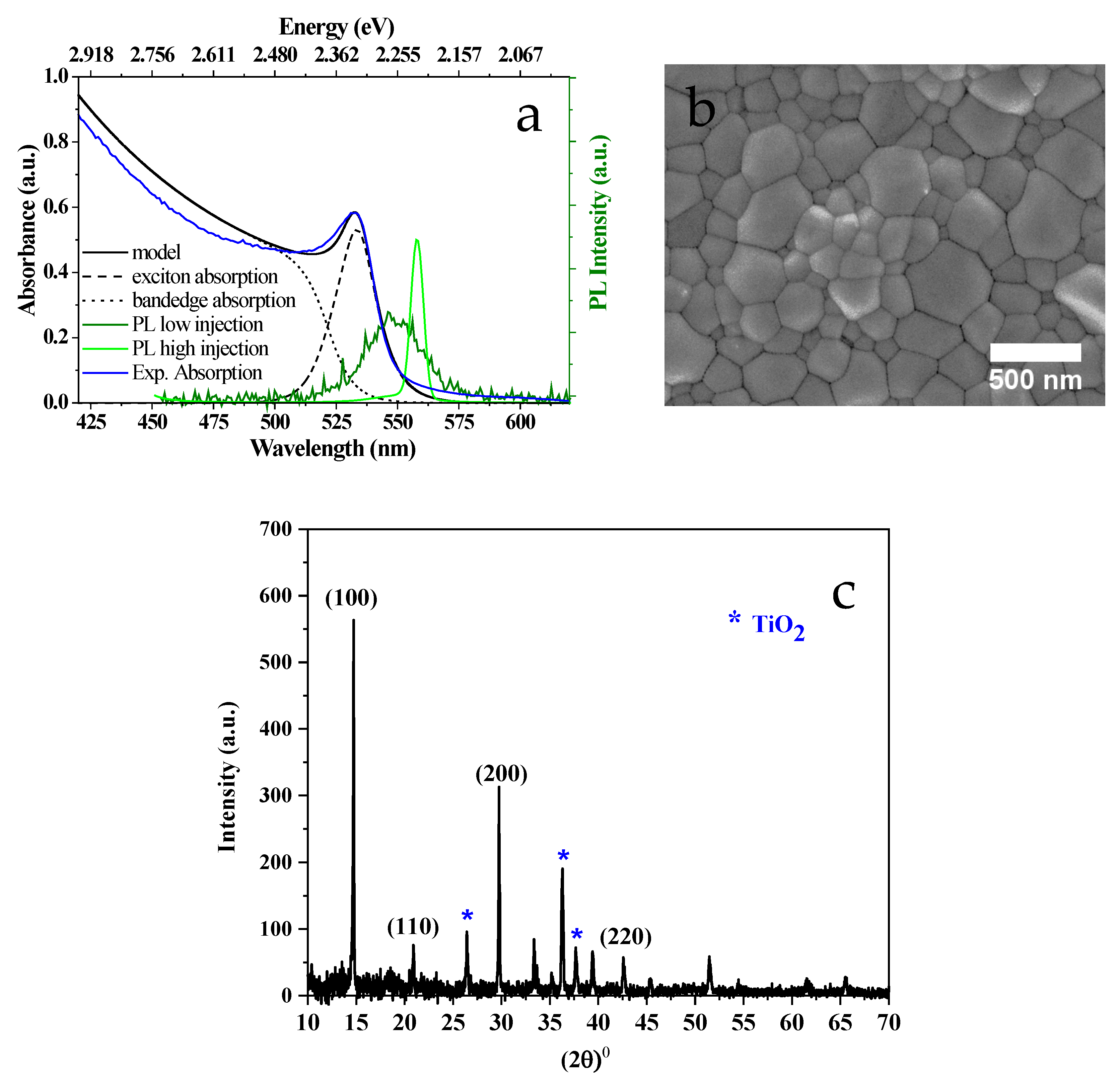
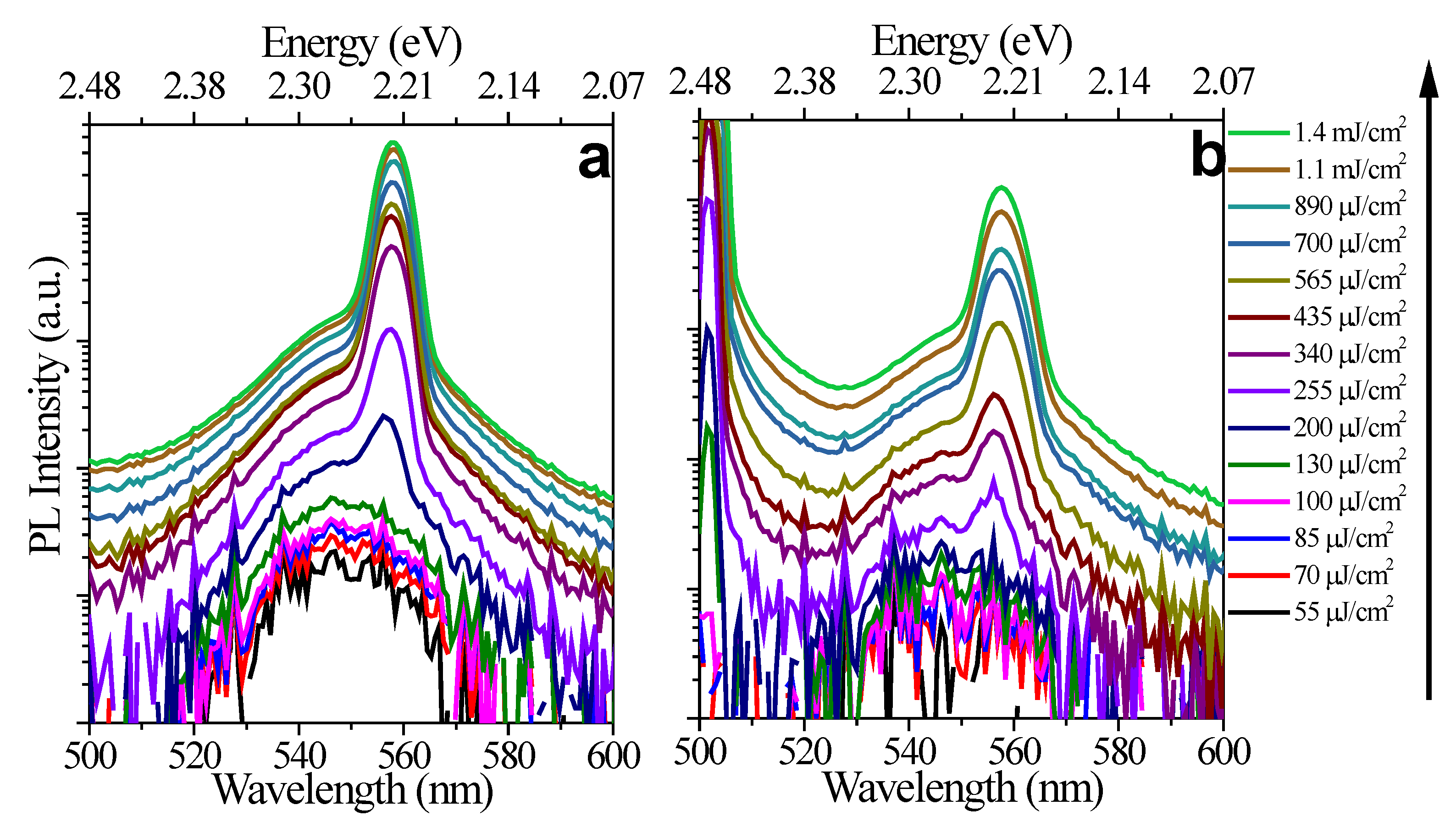
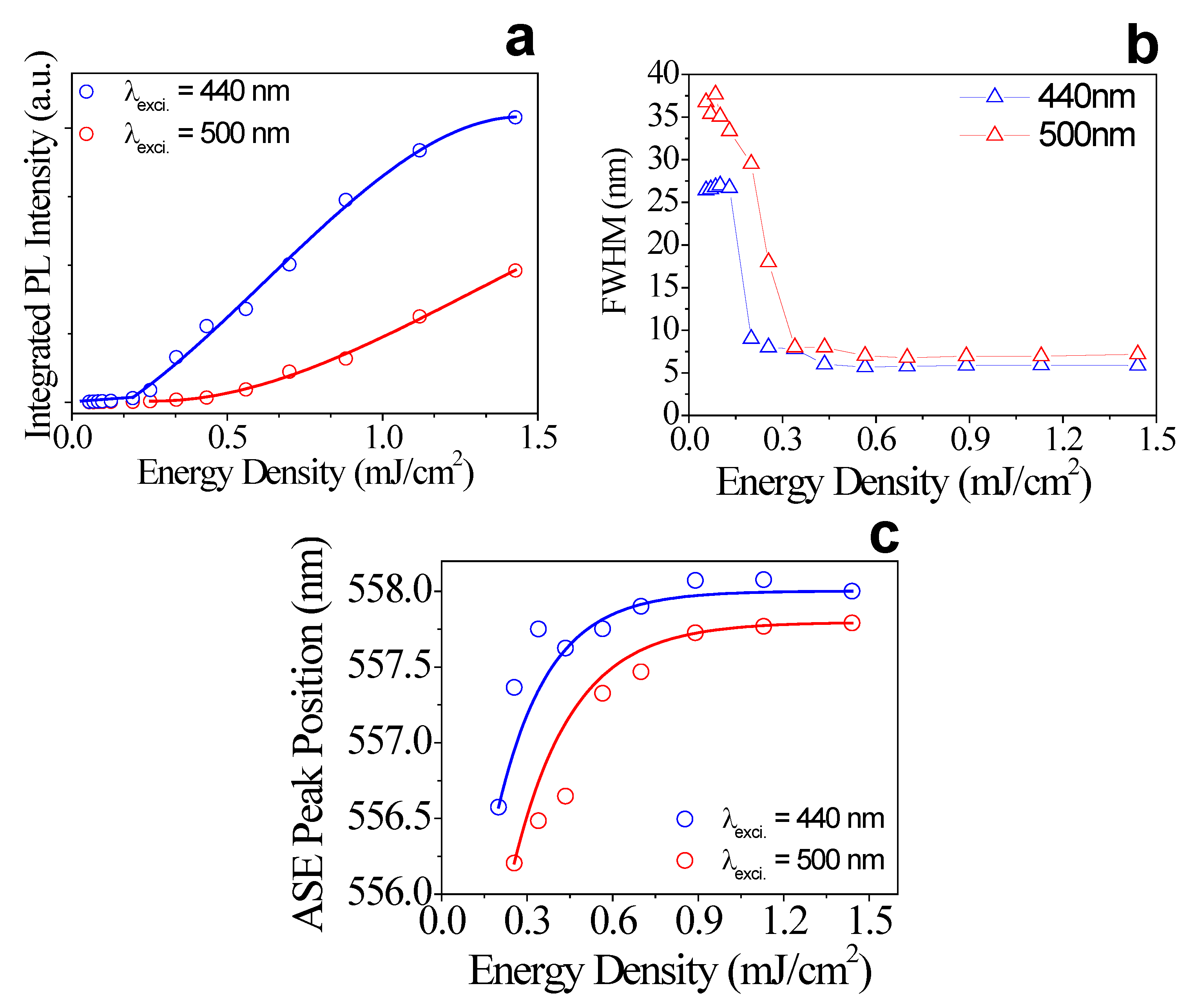
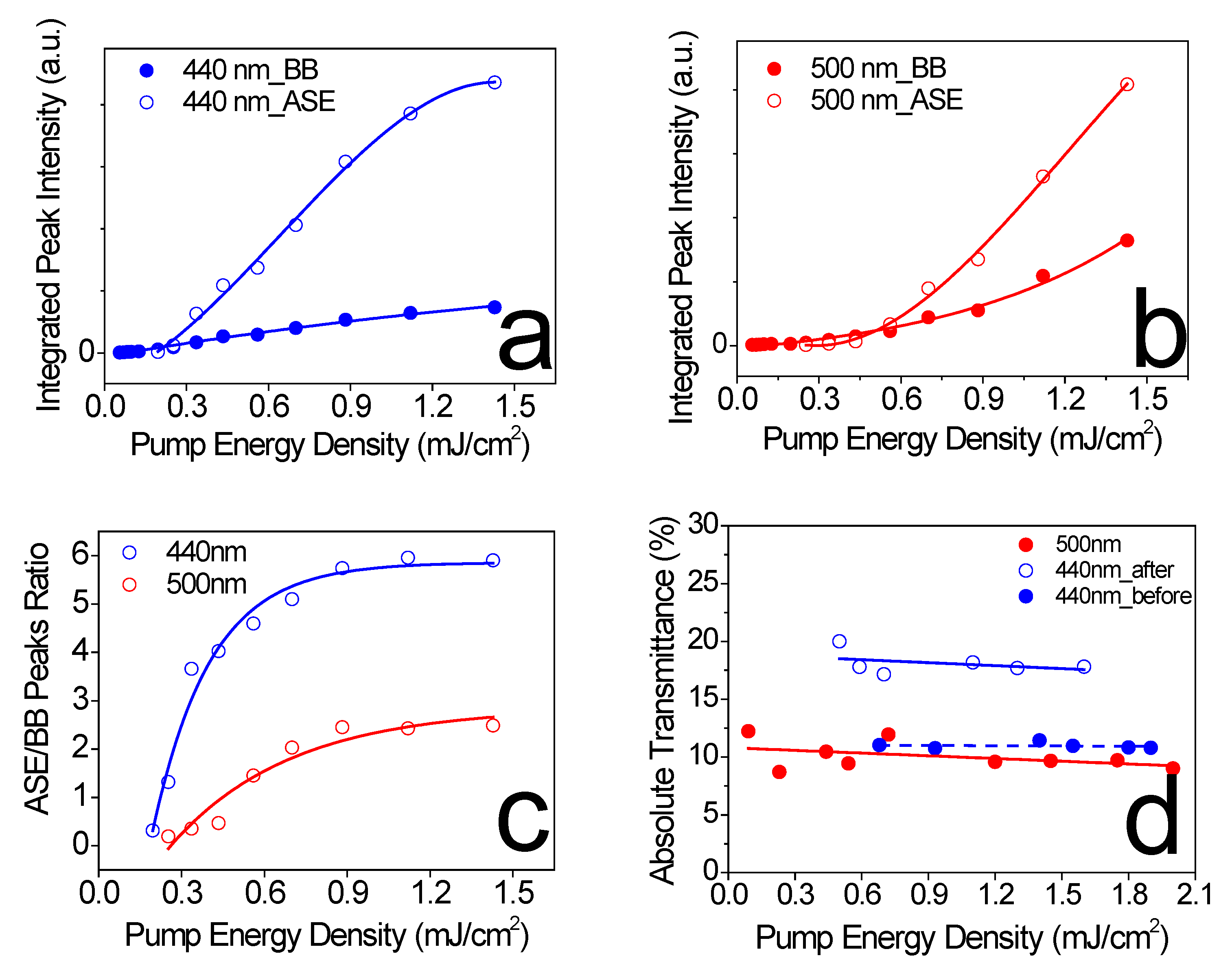
A Beta-Barium Borate Optical Parametric Generator (OPG) (Tunable range, 420–2300 nm) (LT-2215 OPG-PC, LOTTIS II, Minsk, Belarus) operated and pumped by a Q-switched Nd:YAG picosecond laser was used to collect the power-dependent PL and ASE data (LS-2151, LOTTIS II, Minsk, Belarus). The pulses were 70–80 ps long, with a 15 Hz repetition rate. After passing through the OPG, a handy lens focused the circular laser beam to a diameter of around 2 mm. In order to gather the laser excitation pulse from the detector and choose the wavelength emitted from the sample, special filters were utilized. The sample’s output signal was gathered using an optical fiber and a collimating lens connected to A QE65 Pro spectrograph (Ocean Optics, Inc., Dunedin, FL, USA). The laser energy density was attenuated using a variable neutral density filter wheel, and the energy was read using an LM-P-209 coherent thermal sensor head to enable the analysis of the threshold dependency on the energy density. Finally, the data from the ASE experiments were analyzed, and Gaussian fits of dual PL and ASE emission peaks were obtained using a custom python-based tool built by our research group.

3. Results

Figure 1a shows the absorbance spectrum of the sample in the UV–visible region; strong absorption in the UV region was observed, which can be validated by the PL excitation scan [26]. FAPbBr3 Perovskite cannot absorb more visible light, owing to the fact that its absorption edge is located at about 520 nm [27]. As such, it is discovered to have substantial UV absorption and considerable emissions at visible wavelengths. The absorbance spectrum (blue curve) has a decreasing feature with the increase of the wavelength, and it shows an absorption edge at ~520 nm with a sharp peak at 533 nm. This peak indicates the presence of an excitonic transition, and it also indicates the high crystal quality of the film, as shown in Figure 1a,c [28]. Here, the mesoporous layer was introduced, in order to improve the morphology of the subsequently grown FAPbBr3 perovskite layer, and the grain size was ultimately limited by the TiO2 mesoporous network, as discussed in our previous work [29] and some previous reports for other researchers [30]. Furthermore, the XRD pattern of the FAPbBr3 film is deposited onto mesoporous TiO2 (Figure 1c), which then revealed strong and prominent peaks at (2θ) 14.68°, 21.01°, 29.78°, and 42.68°, which matched to diffractions from the (100), (110), (200), and (220) crystal planes, respectively. The XRD spectrum revealed some peaks related to the TiO2 film pattern. The resulting perovskite film’s X-ray diffraction pattern could be indexed to the cubic phase of FAPbBr3 perovskite. The diffraction from the (100) plane at 14.68° was fairly powerful, and its presence, along with the secondary diffraction peak of the (200) plane, indicated the presence of a highly crystalline and defect-free cubic phase [29,31,32].
An absorption background of ~0.3 was subtracted from the absorption spectrum in order to remove the wavelength-independent component of light scattering [33]. As can be seen in the SEM image in Figure 1b, the absorption background was weakly dependent on the wavelength, which may be explained by the Mie scattering of light by the sub-micro grains in the perovskite layer. The absorption spectrum was recalculated using the Elliot formula, as reported by Sestu et al. [34], and the results are also presented in Figure 1a. The best-fitting parameters give a bandgap energy of 2.375 eV, an exciton binding energy of 53 meV (similar to values published by [35,36]), and an exciton peak broadening of 70 meV.
Excitation wavelengths of 440 nm and 500 nm, which correspond to optical densities of 0.71 and 0.47, respectively, were used in the amplified spontaneous emission (ASE) experiments. Figure 2a,b shows the PL spectra evolution, indicating the presence of two regimes from Spontaneous Emission (SE) to ASE, with increasing the pump energy density under the two excitation wavelengths. Below the threshold energy densities, PL shows relatively broad emission spectra centered at 544 nm under both excitations. Above the threshold, as reported previously [12,20,37,38], this broad emission is split with the emergence of a narrower peak at ~ 556 nm, which characterizes the ASE state.
The origin of the two peaks in distinct perovskite materials has received little attention in the literature [12,15,37,38]. Following Ding and co-workers [39] thorough studies on (Zn,Cd)Se/ZnSe quantum well lasers, Xing et al. [15] suggested the presence of ASE at the lower energy side of the exciton band, even below the Mott transition limit. Although a definite excitonic band can be detected in our sample (see Figure 1a), perovskite materials may not meet the other requirements required by [39] to have such excitonic gain. In particular, in perovskite materials [40,41,42], the criterion of having considerable inhomogeneous broadening compared to homogeneous thermal broadening [39] is not met. Biexcitons were blamed by Kondo et al. for the formation of the lower-energy ASE peak [12]. In reality, they used 2D multilayered perovskite in their research, which is well-known for its high exciton binding energies, as was previously indicated. Biexcition production is more likely when the exciton binding energy is higher. This hypothesis is also dubious, given that our 3D perovskite has a one-order-of-magnitude lower exciton binding energy [35,36]. The two peaks, according to Priante et al., are caused by surface imperfections, with the greater energy peak having a limited density of states (DOS) and the lower energy peak having a significantly higher DOS [37]. When the excitation energy is increased, there is no defect-like signature for the broad peak with a limited density of states. In these states, the photogenerated excess carrier starts to fill the accessible states, and then the PL intensities become saturated. This observation backs up the theory that the PL hump is caused by bulk defects [37]. As a result, the PL spectra for this sample only had one narrow peak and one broad hump, both of which were connected to surface states and minor bulk defect recombinations. This result indicates a suitable starting material for light emitters, which is in line with the XRD data shown in Figure 1c. This theory was inspired by the observation that high-quality single crystals only have a single peak [43], whereas polycrystalline samples generated under very mild circumstances had two peaks [37]. Kai Chen et al. [38] investigated ultrafast broadband PL and absorption, and discovered a short-lived (10 ps) PL emission caused by uncorrelated hot carriers above the bandgap. After heated carriers are thermalized, an ASE peak appears on the lower energy side that is stronger and sharper [38]. Indeed, sample preparation procedures can cause very dissimilar behavior in various perovskite samples, with differing origins of the two peaks.
Figure 3a,b depicts the behavior of integrated PL and FWHM as the pump energy density increases for the two excitation wavelengths, respectively. Clearly, the excitation wavelength has a significant impact on the ASE behavior. Varying excitation wavelengths absorb differently depending on the absorption spectrum, resulting in different free carrier densities for the same excitation energy density. As a result, the ASE threshold energy density will follow the absorption spectrum as it varies with the excitation wavelength. The ASE state was achieved with a threshold energy density of ~200 µJ/cm2 under 440 nm excitation. Excitation at 500 nm, on the other hand, needs a higher threshold energy density of ~255 µJ/cm2. The lower slope of the PL vs. pump energy density charts in Figure 3a indicates that excitation with 500 nm results in a slower differential quantum efficiency.
Under both excitation wavelengths, Figure 3c depicts the behavior of the ASE peak position with the pump energy density. The ASE peak redshifts with increasing pump energy densities at both excitation wavelengths. Bandgap renormalization (BGR) in the perovskite crystal under strong excitation is responsible for such characteristics [44]. BGR is a charge carrier many-body problem in semiconductors, in which interactions between electrons and holes under high population conditions cause the bandgap to redshift [45,46]. Over the whole pump energy density range under study, the ASE peak is slightly redshifted by 1.5 nm under both excitations compared to the PL, equating to a bandgap renormalization of ~7–8 meV, as will be detailed later. The small red-shift of the ASE peak can be explained by attractive exciton–exciton interactions, and it also indicates the high crystal quality of the film, as discussed above [28,47,48,49].
The static properties of the integrated PL with the pump energy density for the two emission peaks are shown in Figure 4. Both peaks were fitted with appropriate Gaussian functions using least square fitting. The integrated PL for the two peaks under 440 nm and 500 nm excitations, respectively, is shown in Figure 4a,b. The presence of the well-known spontaneous and stimulated emission areas distinguishes the ASE peak (open circles). Under 440 nm excitation, this categorization is simple to achieve. The delayed ASE increase, however, prevented a distinct beginning of the stimulated emission zone under 500 nm excitation.
Figure 4c compares the integrated PL of the ASE peak to that of the higher energy broad (BB) peak in order to gain a better understanding of the ASE mechanism in our sample. Figure 4c plots the ratio of the two peaks’ areas over the range of the pump energy density (Penergy) where the Bernard Durrafourg condition is likely achieved (Penergy ≥ Eth) under both excitations. Two regions can be distinguished over this pump energy range: a fast-growing ratio over energy range Eth ≤ Penergy ≤ 2 Eth, which is followed by a saturation region above ~2 Eth. The rate of ratio growth is highly dependent on the excitation wavelength. The peaks’ ratio has a faster growth under the 440 nm excitation compared to the 500 nm one.
The absorption behavior of the perovskite layer was further investigated under the high picosecond pulses utilized to induce the ASE in order to correctly quantify the carrier densities involved in our experiments. Absolute transmittance measurements were taken, and a discrepancy between the two excitation wavelengths was discovered. The absolute transmittance findings for both excitations are shown in Figure 4d. Under 440 nm, absolute transmittance begins (solid blue circles) extremely near to that of 500 nm (solid red circles), before rapidly increasing by ~60–70 percent (open blue circles). This increase in transmittance occurs in a matter of seconds under 440 nm stimulation, and it happens even faster under increased excitation power. Absolute transmittance, as well as ASE, stays stable after this rapid increase. The absolute transmittance under 500 nm excitation does not have the same transient behavior as it does under 440 nm excitation. The presence of a highly absorbing surface layer on the perovskite film, which could be removed by the higher-energy 440 nm pulses, is credited with the improvement in absolute transmittance. There have been reports of molecules/complexes adsorbing at the TiO2/perovskite interface or on the perovskite surface, which can have a significant impact on the absorbance and other optical properties of perovskite films [50,51,52]. In order to figure out where this extra layer came from, more enquiries are being carried out.
Figure 5a shows the ASE power dependence as a function of the injected carrier density (n). The carrier density was determined using the absorbance spectrum, taking into consideration the increased absorption of the surface layer under 500 nm excitation. Under both excitations, the spontaneous emission to the ASE state occurs at a distinct onset of 4.5 × 1018 cm−3. Figure 3a shows how the quantum efficiency behaves under both excitations. Both excitations had similar quantum efficiency characteristics, with a slightly lower slope under 440 nm, which might be explained by thermal effects due to increased phonon-assisted photocarrier thermalization.
The bandgap renormalization factor can be calculated using the equation [29,31,44,53]: Δ E B G R = 2   γ   n 1 3 , where γ is the bandgap renormalization factor. The redshift in the emission peak as the pump power increases can be utilized to estimate the BGR at different pump powers. Indeed, the ASE is expected to appear at the gain region’s highest point. The position of this maximum as a function of the carrier density in a bulk material is nearly constant, as the absorption has a steplike function due to the Sommerfeld amplification factor [44].
The graphs of Δ E B G R vs. n 1 3 for the two excitation wavelengths are shown in Figure 5b. BGR rises as the carrier density rises, as one would expect. At a pump energy density of ~0.9 mJ/cm2, a maximum BGR value of ~7–8 meV is reached, equivalent to a maximum red-shift of 1.5 nm. This tiny BGR is expected for unconfined photocarriers in a three-dimensional framework. The BGR becomes saturated at higher pump energy densities (greater than 0.9 mJ/cm2). Different scattering and other gain losses can likely occur in a gain-clamping state due to the 3D and cavity-free structure of our sample and the comparatively large laser spot size of 2 mm.
Gain clamping prevents the carrier density from increasing significantly as the fluence is increased. Because the BGR is solely dependent on the carrier density, the energy shift is essentially undetectable above 0.9 mJ/cm2, which is further obscured by the spectral resolution of 0.16 nm in our setup. As a result, only the lower carrier density values were used to calculate the bandgap renormalization coefficient, which was found to be ~5–7 × 10⁻⁹ eV cm for both excitations. This bandgap renormalization coefficient value is very close to the GaAs values reported in the literature [44].
Our findings show that, despite its unresolved stability difficulties, perovskite behaves similarly to a typical semiconductor, and can thus be handled further using the same formalisms. Finally, in Table 1 below, some of the numbers stated in the document are listed.
As a result, we may trace back the variation of the bandgap as a function of the carrier density by tracing the ASE peak position as a function of the fluence. In order to better understand this behavior, gain vs. energy curves are plotted in Figure 6 using the values of carrier effective masses (electrons and holes) retrieved from [54] for FAPbBr3, as well as the exciton binding energy of 53 meV computed above. At the band edge absorption spectrum in Figure 1, the steplike behavior of the gain function can be seen to be more evident at larger carrier densities, resulting in the ASE peak reflecting the bandgap behavior as well.

4. Conclusions

Using picosecond laser pulses with various absorbed excitation wavelengths of 440 nm and 500 nm, the ASE evolution of a cavity-free high quality FAPbBr3 perovskite layer was examined. Thermal effects linked with increased energy and heavily absorbed 440 nm pulses had a minimal effect on the quantum efficiency, according to power-dependent PL observations. A strongly absorbing surface layer was observed, confirming the perovskite surface’s claimed great sensitivity to the environment. The ASE state was achieved with a threshold energy density of ~200 µJ/cm2 under 440 nm excitation. Excitation at 500 nm, on the other hand, needs a higher threshold energy density of ~255 µJ/cm2. For the FAPbBr3 film, the BGR was calculated, yielding a BGR constant of ~5–7 × 10⁻⁹ eV cm.

Author Contributions

Conceptualization, S.M.H.Q. and A.S.A.; methodology, S.M.H.Q.; software, S.M.H.Q.; validation, S.M.H.Q. and A.S.A.; formal analysis, S.M.H.Q.; investigation, S.M.H.Q., H.M.G., K.K.A., A.F.B.A., B.A.A.-A. and A.S.A.; resources, S.M.H.Q. and A.S.A.; data curation, S.M.H.Q.; writing—original draft preparation, S.M.H.Q. and A.S.A.; writing—review and editing, A.S.A., S.M.H.Q., H.M.G., K.K.A., A.F.B.A. and B.A.A.-A.; visualization, S.M.H.Q.; supervision, S.M.H.Q. and A.S.A.; project administration, S.M.H.Q. and A.S.A.; funding acquisition, S.M.H.Q. and A.S.A. All authors have read and agreed to the published version of the manuscript.

Funding

This project was funded by the National Plan for Science, Technology and Innovation (MAARIFAH), King Abdulaziz City for Science and Technology, Kingdom of Saudi Arabia, Award Number (15-ELE3793-02).

Data Availability Statement

The data presented in this study are available on request from the corresponding author.

Conflicts of Interest

The authors declare no conflict of interest.

References

  1. Xing, G.; Mathews, N.; Sun, S.; Lim, S.S.; Lam, Y.M.; Grätzel, M.; Mhaisalkar, S.; Sum, T.C. Long-range balanced electron- and hole-transport lengths in organic-inorganic CH3NH3PbI3. Science 2013, 342, 344–347. [Google Scholar] [CrossRef]
  2. Kim, H.S.; Lee, C.R.; Im, J.H.; Lee, K.B.; Moehl, T.; Marchioro, A.; Moon, S.J.; Humphry-Baker, R.; Yum, J.H.; Moser, J.E.; et al. Lead iodide perovskite sensitized all-solid-state submicron thin film mesoscopic solar cell with efficiency exceeding 9%. Sci. Rep. 2012, 2, 591. [Google Scholar] [CrossRef] [PubMed] [Green Version]
  3. Heo, J.H.; Im, S.H.; Noh, J.H.; Mandal, T.N.; Lim, C.-S.; Chang, J.A.; Lee, Y.H.; Kim, H.; Sarkar, A.; Nazeeruddin, K.; et al. Efficient inorganic-organic hybrid heterojunction solar cells containing perovskite compound and polymeric hole conductors. Nat. Photonics 2013, 7, 486–491. [Google Scholar] [CrossRef]
  4. Burschka, J.; Pellet, N.; Moon, S.-J.; Humphry-Baker, R.; Gao, P.; Nazeeruddin, M.K.; Grätzel, M. Sequential deposition as a route to high-performance perovskite-sensitized solar cells. Nature 2013, 499, 316–319. [Google Scholar] [CrossRef] [PubMed]
  5. Wehrenfennig, C.; Eperon, G.E.; Johnston, M.B.; Snaith, H.J.; Herz, L.M. High charge carrier mobilities and lifetimes in organolead trihalide perovskites. Adv. Mater. 2014, 26, 1584–1589. [Google Scholar] [CrossRef] [Green Version]
  6. Alcocer, M.J.P.; Leijtens, T.; Herz, L.M.; Petrozza, A.; Snaith, H.J. Electron-Hole Diffusion Lengths Exceeding 1 Micrometer in an Organometal Trihalide Perovskite Absorber. Science 2014, 342, 341–344. [Google Scholar]
  7. Papavassiliou, G.C.; Koutselas, I.B. Structural, optical and related properties of some natural three- and lower-dimensional semiconductor systems. Synth. Met. 1995, 71, 1713–1714. [Google Scholar] [CrossRef]
  8. Chondroudis, K.; Kagan, C.R. Organic-inorganic electronics. IBM J. Res. Dev. 2001, 45, 29–45. [Google Scholar]
  9. Mitzi, D.B.; Feild, C.A.; Schlesinger, Z.; Laibowitz, R.B. Transport, Optical, and Magnetic Properties of the Conducting Halide Perovskite CH3NH3SnI3. J. Solid State Chem. 1995, 114, 159–163. [Google Scholar] [CrossRef]
  10. Chondroudis, K.; Mitzi, D.B. Electroluminescence from an Organic-Inorganic Perovskite Incorporating a Quaterthiophene Dye within Lead Halide Perovskite Layers. Chem. Mater. 1999, 11, 3028–3030. [Google Scholar] [CrossRef]
  11. Baikie, T.; Fang, Y.; Kadro, J.M.; Schreyer, M.; Wei, F.; Mhaisalkar, S.G.; Gratzel, M.; White, T.J. Synthesis and crystal chemistry of the hybrid perovskite (CH3NH3)PbI3 for solid-state sensitised solar cell applications. J. Mater. Chem. A 2013, 1, 5628. [Google Scholar] [CrossRef]
  12. Kondo, T.; Azuma, T.; Yuasa, T.; Ito, R. Biexciton lasing in the layered perovskite-type material (C6H13NH3)2PbI4. Solid State Commun. 1998, 105, 253–255. [Google Scholar] [CrossRef]
  13. Tan, Z.-K.; Moghaddam, R.S.; Lai, M.L.; Docampo, P.; Higler, R.; Deschler, F.; Price, M.; Sadhanala, A.; Pazos, L.M.; Credgington, D.; et al. Bright light-emitting diodes based on organometal halide perovskite. Nat. Nanotechnol. 2014, 9, 687–692. [Google Scholar] [CrossRef] [PubMed]
  14. Deschler, F.; Price, M.; Pathak, S.; Klintberg, L.E.; Jarausch, D.-D.; Higler, R.; Hüttner, S.; Leijtens, T.; Stranks, S.D.; Snaith, H.J.; et al. High photoluminescence efficiency and optically pumped lasing in solution-processed mixed halide perovskite semiconductors. J. Phys. Chem. Lett. 2014, 5, 1421–1426. [Google Scholar] [CrossRef]
  15. Xing, G.; Mathews, N.; Lim, S.S.; Yantara, N.; Liu, X.; Sabba, D.; Grätzel, M.; Mhaisalkar, S.; Sum, T.C. Low-temperature solution-processed wavelength-tunable perovskites for lasing. Nat. Mater. 2014, 13, 476–480. [Google Scholar] [CrossRef]
  16. Zhang, Q.; Ha, S.T.; Liu, X.; Sum, T.C.; Xiong, Q. Room-temperature near-infrared high-Q perovskite whispering-gallery planar nanolasers. Nano Lett. 2014, 14, 5995–6001. [Google Scholar] [CrossRef] [PubMed]
  17. Dhanker, R.; Brigeman, A.N.; Larsen, A.V.; Stewart, R.J.; Asbury, J.B.; Giebink, N.C. Random lasing in organo-lead halide perovskite microcrystal networks. Appl. Phys. Lett. 2014, 105, 151112. [Google Scholar] [CrossRef]
  18. Sutherland, B.R.; Hoogland, S.; Adachi, M.M.; Wong, C.T.O.; Sargent, E.H. Conformal organohalide perovskites enable lasing on spherical resonators. ACS Nano 2014, 8, 10947–10952. [Google Scholar] [CrossRef]
  19. Zhu, H.; Fu, Y.; Meng, F.; Wu, X.; Gong, Z.; Ding, Q.; Gustafsson, M.V.; Trinh, M.T.; Jin, S.; Zhu, X.-Y. Lead halide perovskite nanowire lasers with low lasing thresholds and high quality factors. Nat. Mater. 2015, 14, 636–642. [Google Scholar] [CrossRef]
  20. Arora, N.; Dar, M.I.; Hezam, M.; Tress, W.; Jacopin, G.; Moehl, T.; Gao, P.; Aldwayyan, A.S.; Deveaud, B.; Grätzel, M.; et al. Photovoltaic and Amplified Spontaneous Emission Studies of High-Quality Formamidinium Lead Bromide Perovskite Films. Adv. Funct. Mater. 2016, 26, 2846–2854. [Google Scholar] [CrossRef]
  21. Amat, A.; Mosconi, E.; Ronca, E.; Quarti, C.; Umari, P.; Nazeeruddin, M.K.; Grätzel, M.; De Angelis, F. Cation-induced band-gap tuning in organohalide perovskites: Interplay of spin-orbit coupling and octahedra tilting. Nano Lett. 2014, 14, 3608–3616. [Google Scholar] [CrossRef] [PubMed]
  22. Aygüler, M.F.; Weber, M.D.; Puscher, B.M.D.; Medina, D.D.; Docampo, P.; Costa, R.D. Light-Emitting Electrochemical Cells Based on Hybrid Lead Halide Perovskite Nanoparticles. J. Phys. Chem. C 2015, 119, 12047–12054. [Google Scholar] [CrossRef] [Green Version]
  23. Eperon, G.E.; Bryant, D.; Troughton, J.; Stranks, S.D.; Johnston, M.B.; Watson, T.; Worsley, D.A.; Snaith, H.J. Efficient, Semitransparent Neutral-Colored Solar Cells Based on Microstructured Formamidinium Lead Trihalide Perovskite. J. Phys. Chem. Lett. 2015, 6, 129–138. [Google Scholar] [CrossRef]
  24. Hanusch, F.C.; Wiesenmayer, E.; Mankel, E.; Binek, A.; Angloher, P.; Fraunhofer, C.; Giesbrecht, N.; Feckl, J.M.; Jaegermann, W.; Johrendt, D.; et al. Efficient Planar Heterojunction Perovskite Solar Cells Based on Formamidinium Lead Bromide. J. Phys. Chem. Lett. 2014, 5, 2791–2795. [Google Scholar] [CrossRef] [PubMed]
  25. Auf Der Maur, M.; Pecchia, A.; Penazzi, G.; Rodrigues, W.; Di Carlo, A. Efficiency Drop in Green InGaN/GaN Light Emitting Diodes: The Role of Random Alloy Fluctuations. Phys. Rev. Lett. 2016, 116, 027401. [Google Scholar] [CrossRef] [Green Version]
  26. Kang, C.H.; Dursun, I.; Liu, G.; Sinatra, L.; Sun, X.; Kong, M.; Pan, J.; Maity, P.; Ooi, E.N.; Ng, T.K.; et al. High-speed colour-converting photodetector with all-inorganic CsPbBr3 perovskite nanocrystals for ultraviolet light communication. Light Sci. Appl. 2019, 8, 94. [Google Scholar] [CrossRef] [PubMed]
  27. Wang, Y.; Zhang, Y.; Lu, Y.; Xu, W.; Mu, H.; Chen, C.; Qiao, H.; Song, J.; Li, S.; Sun, B.; et al. Hybrid Graphene-Perovskite Phototransistors with Ultrahigh Responsivity and Gain. Adv. Opt. Mater. 2015, 3, 1389–1396. [Google Scholar] [CrossRef]
  28. Grancini, G.; Srimath Kandada, A.R.; Frost, J.M.; Barker, A.J.; De Bastiani, M.; Gandini, M.; Marras, S.; Lanzani, G.; Walsh, A.; Petrozza, A. Role of microstructure in the electron–hole interaction of hybrid lead halide perovskites. Nat. Photonics 2015, 9, 695–701. [Google Scholar] [CrossRef] [Green Version]
  29. Qaid, S.M.H.; Alharbi, F.H.; Bedja, I.; Nazeeruddin, M.K.; Aldwayyan, A.S. Reducing amplified spontaneous emission threshold in CsPbBr3 quantum dot films by controlling TiO2 compact layer. Nanomaterials 2020, 10, 1605. [Google Scholar] [CrossRef]
  30. Tang, N.; Li, Y.; Chen, F.; Han, Z. In situ fabrication of a direct Z-scheme photocatalyst by immobilizing CdS quantum dots in the channels of graphene-hybridized and supported mesoporous titanium nanocrystals for high photocatalytic performance under visible light. RSC Adv. 2018, 8, 42233–42245. [Google Scholar] [CrossRef] [Green Version]
  31. Qaid, S.M.H.; Ghaithan, H.M.; Al-Asbahi, B.A.; Alqasem, A.; Aldwayyan, A.S. Fabrication of thin films from powdered cesium lead bromide (CsPbBr3) perovskite quantum dots for coherent green light emission. ACS Omega 2020, 5, 30111–30122. [Google Scholar] [CrossRef]
  32. Arora, N.; Dar, M.I.; Abdi-Jalebi, M.; Giordano, F.; Pellet, N.; Jacopin, G.; Friend, R.H.; Zakeeruddin, S.M.; Grätzel, M. Intrinsic and Extrinsic Stability of Formamidinium Lead Bromide Perovskite Solar Cells Yielding High Photovoltage. Nano Lett. 2016, 16, 7155–7162. [Google Scholar] [CrossRef] [PubMed] [Green Version]
  33. Tian, Y.; Scheblykin, I.G. Artifacts in Absorption Measurements of Organometal Halide Perovskite Materials: What Are the Real Spectra? J. Phys. Chem. Lett. 2015, 6, 3466–3470. [Google Scholar] [CrossRef] [Green Version]
  34. Sestu, N.; Cadelano, M.; Sarritzu, V.; Chen, F.; Marongiu, D.; Piras, R.; Mainas, M.; Quochi, F.; Saba, M.; Mura, A.; et al. Absorption F-Sum Rule for the Exciton Binding Energy in Methylammonium Lead Halide Perovskites. J. Phys. Chem. Lett. 2015, 6, 4566–4572. [Google Scholar] [CrossRef] [PubMed]
  35. Kitazawa, N.; Watanabe, Y.; Nakamura, Y. Optical properties of CH3NH3PbX3 (X = halogen) and their mixed-halide crystals. J. Mater. Sci. 2002, 37, 3585–3587. [Google Scholar] [CrossRef]
  36. D’Innocenzo, V.; Grancini, G.; Alcocer, M.J.P.; Kandada, A.R.S.; Stranks, S.D.; Lee, M.M.; Lanzani, G.; Snaith, H.J.; Petrozza, A. Excitons versus free charges in organo-lead tri-halide perovskites. Nat. Commun. 2014, 5, 045214. [Google Scholar] [CrossRef] [PubMed] [Green Version]
  37. Priante, D.; Dursun, I.; Alias, M.S.; Shi, D.; Melnikov, V.A.; Ng, T.K.; Mohammed, O.F.; Bakr, O.M.; Ooi, B.S. The recombination mechanisms leading to amplified spontaneous emission at the true-green wavelength in CH3NH3PbBr3 perovskites. Appl. Phys. Lett. 2015, 106, 1–5. [Google Scholar] [CrossRef] [Green Version]
  38. Chen, K.; Barker, A.J.; Morgan, F.L.C.; Halpert, J.E.; Hodgkiss, J.M. Effect of carrier thermalization dynamics on light emission and amplification in organometal halide perovskites. J. Phys. Chem. Lett. 2015, 6, 153–158. [Google Scholar] [CrossRef]
  39. Ding, J.; Hagerott, M.; Ishihara, T.; Jeon, H.; Nurmikko, A.V. (Zn,Cd)Se/ZnSe quantum-well lasers: Excitonic gain in an inhomogeneously broadened quasi-two-dimensional system. Phys. Rev. B 1993, 47, 10528–10542. [Google Scholar] [CrossRef] [PubMed]
  40. Wehrenfennig, C.; Liu, M.; Snaith, H.J.; Johnston, M.B.; Herz, L.M. Homogeneous emission line broadening in the organo lead halide perovskite CH3NH3PbI3-xClx. J. Phys. Chem. Lett. 2014, 5, 1300–1306. [Google Scholar] [CrossRef] [PubMed]
  41. Wu, K.; Bera, A.; Ma, C.; Du, Y.; Yang, Y.; Li, L.; Wu, T. Temperature-dependent excitonic photoluminescence of hybrid organometal halide perovskite films. Phys. Chem. Chem. Phys. 2014, 16, 22476–22481. [Google Scholar] [CrossRef]
  42. Kunugita, H.; Hashimoto, T.; Kiyota, Y.; Udagawa, Y.; Takeoka, Y.; Nakamura, Y.; Sano, J.; Matsushita, T.; Kondo, T.; Miyasaka, T.; et al. Excitonic Feature in Hybrid Perovskite CH3NH3PbBr3 single crystals. Chem. Lett. 2015, 44, 852–854. [Google Scholar] [CrossRef]
  43. Shi, D.; Adinolfi, V.; Comin, R.; Yuan, M.; Alarousu, E.; Buin, A.; Chen, Y.; Hoogland, S.; Rothenberger, A.; Katsiev, K.; et al. Low trap-state density and long carrier diffusion in organolead trihalide perovskite single crystals. Science 2015, 347, 519–522. [Google Scholar] [CrossRef] [Green Version]
  44. Yang, Y.; Ostrowski, D.P.; France, R.M.; Zhu, K.; van de Lagemaat, J.; Luther, J.M.; Beard, M.C. Observation of a hot-phonon bottleneck in lead-iodide perovskites. Nat. Photonics 2015, 10, 1–7. [Google Scholar] [CrossRef]
  45. Brinkman, W.F.; Rice, T.M. Electron-Hole Liquids in Semiconductors. Phys. Rev. B 1973, 7, 1508–1523. [Google Scholar] [CrossRef]
  46. Tränkle, G.; Leier, H.; Forchel, A.; Haug, H.; Ell, C.; Weimann, G. Dimensionality dependence of the band-gap renormalization in two- and three-dimensional electron-hole plasmas in GaAs. Phys. Rev. Lett. 1987, 58, 419–422. [Google Scholar] [CrossRef]
  47. Di Stasio, F.; Grim, J.Q.; Lesnyak, V.; Rastogi, P.; Manna, L.; Moreels, I.; Krahne, R. Single-Mode Lasing from Colloidal Water-Soluble CdSe/CdS Quantum Dot-in-Rods. Small 2015, 11, 1328–1334. [Google Scholar] [CrossRef] [Green Version]
  48. Delikanli, S.; Isik, F.; Shabani, F.; Baruj, H.D.; Taghipour, N.; Demir, H.V. Ultralow Threshold Optical Gain Enabled by Quantum Rings of Inverted Type-I CdS/CdSe Core/Crown Nanoplatelets in the Blue. Adv. Opt. Mater. 2021, 9, 1–6. [Google Scholar] [CrossRef]
  49. Kelestemur, Y.; Cihan, A.F.; Guzelturk, B.; Demir, H.V. Type-tunable amplified spontaneous emission from core-seeded CdSe/CdS nanorods controlled by exciton-exciton interaction. Nanoscale 2014, 6, 8509–8514. [Google Scholar] [CrossRef] [Green Version]
  50. Leijtens, T.; Eperon, G.E.; Pathak, S.; Abate, A.; Lee, M.M.; Snaith, H.J. Overcoming ultraviolet light instability of sensitized TiO2 with meso-superstructured organometal tri-halide perovskite solar cells. Nat. Commun. 2013, 4, 2885. [Google Scholar] [CrossRef]
  51. Ma, T.; Tadaki, D.; Sakuraba, M.; Sato, S.; Hirano-Iwata, A.; Niwano, M. Effects of interfacial chemical states on the performance of perovskite solar cells. J. Mater. Chem. A 2016, 4, 4392–4397. [Google Scholar] [CrossRef]
  52. Shirayama, M.; Kato, M.; Miyadera, T.; Sugita, T.; Fujiseki, T.; Hara, S.; Kadowaki, H.; Murata, D.; Chikamatsu, M.; Fujiwara, H. Degradation mechanism of CH3NH3PbI3 perovskite materials upon exposure to humid air. J. Appl. Phys. 2016, 119, 115501. [Google Scholar] [CrossRef] [Green Version]
  53. Qaid, S.M.H.; Khan, M.N.; Alqasem, A.; Hezam, M.; Aldwayyan, A. Restraining effect of film thickness on the behaviour of amplified spontaneous emission from methylammonium lead iodide perovskite. IET Optoelectron. 2018, 13, 2–6. [Google Scholar] [CrossRef]
  54. Kumawat, N.K.; Tripathi, M.N.; Waghmare, U.; Kabra, D. Structural, optical, and electronic properties of wide bandgap perovskites: Experimental and theoretical investigations. J. Phys. Chem. A 2016, 120, 3917–3923. [Google Scholar] [CrossRef] [PubMed]
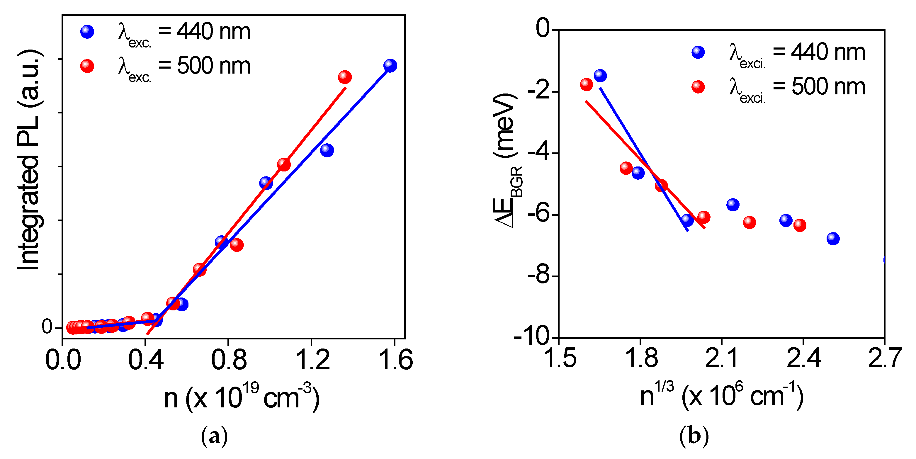
Figure 1. (a) The FAPbBr3 film’s absorbance and PL spectra. In the black line, the computed bandgap and exciton absorption spectra, as well as their summed spectrum, are depicted. For comparison, two PL spectra at low and high pump energy densities are given in green. The Two PL spectra are not to scale. (b) The FAPbBr3 film’s plan view SEM image, and (c) the XRD pattern of the FAPbBr3 film deposited onto mesoporous TiO2.
Photonics 09 00004 g001
Figure 2. Evolution of the PL spectra with a pulse energy density under (a) 440 nm and (b) 500 nm excitation.
Photonics 09 00004 g002
Figure 3. Integrated PL intensity (a), FWHM (b), and ASE peak position (c) vs. the pulse energy density under both excitation wavelengths.
Photonics 09 00004 g003
Figure 4. (a,b) Results of Gaussian fitting for integrated PL vs. the pump energy density for both broad band (BB) and ASE peaks under (a) 440 nm excitation and (b) 500 nm excitation; (c) plot of the ASE/BB peaks’ ratios under different pump energy densities; (d) absolute transmittance for the FAPbBr3/ms-TiO2/FTO sample vs. pump energy densities. Absolute transmittance rapidly increases from the level of blue solid circles to that of blue open circles under 440 nm illumination, as indicated in the text.
Photonics 09 00004 g004
Figure 5. (a) Integrated PL versus the injected carrier density n, and (b) BGR versus n1/3 under both 440 nm and 500 nm excitations.
Photonics 09 00004 g005
Figure 6. Gain vs. energy curves retrieved for different carrier densities.
Photonics 09 00004 g006
Table 1. A summary of the important parameters mentioned in the manuscript.
ExcitationEth (µJ/cm2)Carrier Density (cm−3) Δ E B G R (meV) γ (eV)
440 nm2000.45 × 101977 × 10−9
500 nm2550.45 × 101985 × 10−9
Publisher’s Note: MDPI stays neutral with regard to jurisdictional claims in published maps and institutional affiliations.

