Broadband Polarization Rotator and Splitter Based on 70 nm-Etched Waveguides on SOI Platform


Abstract
:1. Introduction
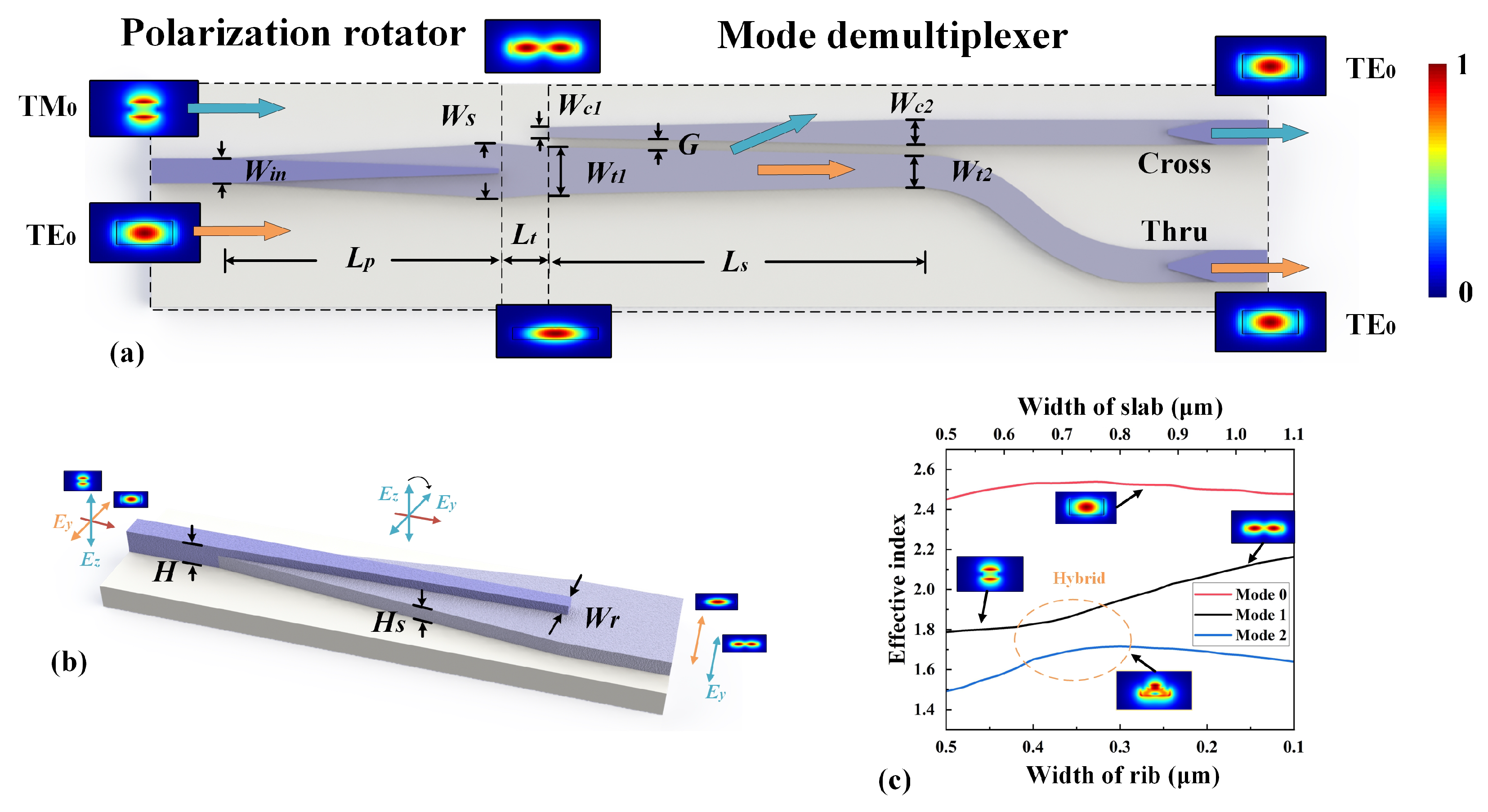
2. Device Design
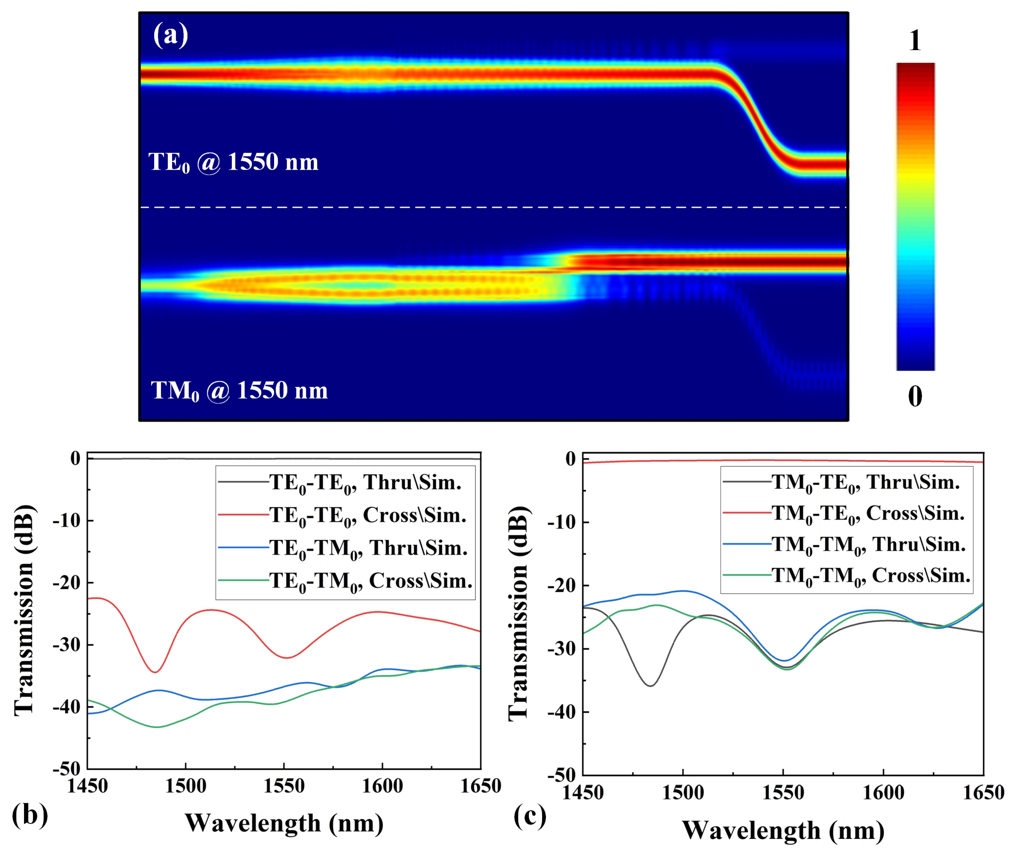
3. Fabrication and Measurement
4. Conclusions
Author Contributions
Funding
Institutional Review Board Statement
Informed Consent Statement
Data Availability Statement
Acknowledgments
Conflicts of Interest
References
- Baehr-Jones, T.; Pinguet, T.; Lo Guo-Qiang, P.; Danziger, S.; Prather, D.; Hochberg, M. Myths and rumours of silicon photonics. Nat. Photonics 2012, 6, 206–208. [Google Scholar] [CrossRef]
- Shi, W.; Tian, Y.; Gervais, A. Scaling capacity of fiber-optic transmission systems via silicon photonics. Nanophotonics 2020, 9, 4629–4663. [Google Scholar] [CrossRef]
- Tian, Y.; Qiu, J.; Liu, C.; Tian, S.; Huang, Z.; Wu, J. Compact polarization beam splitter with a high extinction ratio over S+ C+ L band. Opt. Express 2019, 27, 999–1009. [Google Scholar] [CrossRef] [PubMed]
- Mao, S.; Cheng, L.; Zhao, C.; Fu, H. Ultra-broadband and ultra-compact polarization beam splitter based on a tapered subwavelength-grating waveguide and slot waveguide. Opt. Express 2021, 29, 28066–28077. [Google Scholar] [CrossRef] [PubMed]
- Li, C.; Dai, D.; Bowers, J.E. Ultra-broadband and low-loss polarization beam splitter on silicon. In Optical Fiber Communication Conference; Optical Society of America: Washington, DC, USA, 2020; p. Th1A.4. [Google Scholar]
- Ao, X.; He, S. Polarization beam splitters based on a two-dimensional photonic crystal of negative refraction. Opt. Lett. 2005, 30, 2152–2154. [Google Scholar] [CrossRef] [PubMed]
- Wu, F.; Chen, M.; Xiao, S. Wide-angle polarization selectivity based on anomalous defect mode in photonic crystal containing hyperbolic metamaterials. Opt. Lett. 2022, 47, 2153–2156. [Google Scholar] [CrossRef] [PubMed]
- Shi, X.; Zhang, J.; Fan, W.; Lu, Y.; Peng, N.; Rottwitt, K.; Ou, H. Compact low-birefringence polarization beam splitter using vertical-dual-slot waveguides in silicon carbide integrated platforms. Photonics Res. 2022, 10, A8–A13. [Google Scholar] [CrossRef]
- Zhang, J.; Shi, X.; Zhang, Z.; Guo, K.; Yang, J. Ultra-compact, efficient and high-polarization-extinction-ratio polarization beam splitters based on photonic anisotropic metamaterials. Opt. Express 2022, 30, 538–549. [Google Scholar] [CrossRef]
- Yu, Z.; Xu, H.; Liu, D.; Li, H.; Shi, Y.; Dai, D. Subwavelength-Structure-Assisted Ultracompact Polarization-Handling Components on Silicon. J. Light. Technol. 2022, 40, 1784–1801. [Google Scholar] [CrossRef]
- Liu, C.; Qiu, J.; Tian, Y.; Guo, H.; Hong, X.; Wu, J. Performance Enhancement of a Broadband Polarization Rotator by using Modified Mode Converters. In Asia Communications and Photonics Conference; Optical Society of America: Washington, DC, USA, 2018; p. Su2A–171. [Google Scholar]
- Xu, H.; Shi, Y. Subwavelength-grating-assisted silicon polarization rotator covering all optical communication bands. Opt. Express 2019, 27, 5588–5597. [Google Scholar] [CrossRef]
- Lebbe, N.; Glière, A.; Hassan, K. High-efficiency and broadband photonic polarization rotator based on multilevel shape optimization. Opt. Lett. 2019, 44, 1960–1963. [Google Scholar] [CrossRef] [Green Version]
- Gallacher, K.; Griffin, P.F.; Riis, E.; Sorel, M.; Paul, D.J. Silicon nitride waveguide polarization rotator and polarization beam splitter for chip-scale atomic systems. APL Photonics 2022, 7, 046101. [Google Scholar] [CrossRef]
- Yan, X.; Chen, J.; Dai, D.; Shi, Y. Polarization multiplexing silicon-photonic optical phased array for 2D wide-angle optical beam steering. IEEE Photonics J. 2021, 13, 1–6. [Google Scholar] [CrossRef]
- Dong, P.; Chen, Y.K.; Duan, G.H.; Neilson, D.T. Silicon photonic devices and integrated circuits. Nanophotonics 2014, 3, 215–228. [Google Scholar] [CrossRef]
- Ma, M.; Park, A.H.; Wang, Y.; Shoman, H.; Zhang, F.; Jaeger, N.A.; Chrostowski, L. Sub-wavelength grating-assisted polarization splitter-rotators for silicon-on-insulator platforms. Opt. Express 2019, 27, 17581–17591. [Google Scholar] [CrossRef]
- Zhang, Y.; Zhu, Q.; He, Y.; Su, Y. Silicon polarization splitter and rotator with tolerance to width variations using a nonlinearly-tapered and partially-etched directional coupler. In Optical Fiber Communication Conference; Optical Society of America: Washington, DC, USA, 2019; p. W1E.4. [Google Scholar]
- Xie, C.; Zou, X.; Zou, F.; Zhang, Y. High-performance ultra-compact polarization splitter-rotators based on dual-etching and tapered asymmetrical directional coupler. Chin. Opt. Lett. 2021, 19, 121301. [Google Scholar] [CrossRef]
- Sacher, W.D.; Barwicz, T.; Taylor, B.J.; Poon, J.K. Polarization rotator-splitters in standard active silicon photonics platforms. Opt. Express 2014, 22, 3777–3786. [Google Scholar] [CrossRef] [Green Version]
- Chen, X.; Qiu, C.; Sheng, Z.; Wu, A.; Huang, H.; Zhao, Y.; Li, W.; Wang, X.; Zou, S.; Gan, F.; et al. Design of an ultra-broadband and fabrication-tolerant silicon polarization rotator splitter with SiO2 top cladding. Chin. Opt. Lett. 2016, 14, 081301–81305. [Google Scholar] [CrossRef] [Green Version]
- Zhao, Y.; Qiu, C.; Wu, A.; Huang, H.; Li, J.; Sheng, Z.; Li, W.; Wang, X.; Gan, F. Broadband polarization splitter-rotator and the application in WDM receiver. IEEE Photonics J. 2018, 11, 1–10. [Google Scholar] [CrossRef]
- El-Fiky, E.; Wang, Y.; Bernal, S.; Gamache, C.; Panorel, E.; Kumar, A.; Samani, A.; Jacques, M.; Koh, P.c.; Plant, D.V. High extinction ratio and broadband O-band polarization splitter and rotator on silicon-on-insulator. In Proceedings of the 2019 Optical Fiber Communications Conference and Exhibition (OFC), San Diego, CA, USA, 3–7 March 2019; pp. 1–3. [Google Scholar]
- Chen, Z.; Yang, J.; Wong, W.H.; Pun, E.Y.B.; Wang, C. Broadband adiabatic polarization rotator-splitter based on a lithium niobate on insulator platform. Photonics Res. 2021, 9, 2319–2324. [Google Scholar] [CrossRef]
- Sun, C.; Yu, Y.; Chen, G.; Zhang, X. A low crosstalk and broadband polarization rotator and splitter based on adiabatic couplers. IEEE Photonics Technol. Lett. 2016, 28, 2253–2256. [Google Scholar] [CrossRef]
- Rostamian, A.; Guo, J.; Chakravarty, S.; Yan, H.; Chung, C.J.; Heidari, E.; Chen, R.T. Grating-coupled silicon-on-sapphire polarization rotator operating at mid-infrared wavelengths. IEEE Photonics Technol. Lett. 2019, 31, 401–404. [Google Scholar] [CrossRef]
- Chen, D.; Liu, M.; Zhang, Y.; Wang, L.; Hu, X.; Feng, P.; Xiao, X.; Yu, S. C+ L band polarization rotator-splitter based on a compact S-bend waveguide mode demultiplexer. Opt. Express 2021, 29, 10949–10957. [Google Scholar] [CrossRef]
- Dai, D.; Wu, H. Realization of a compact polarization splitter-rotator on silicon. Opt. Lett. 2016, 41, 2346–2349. [Google Scholar] [CrossRef]
- Guo, D.; Chu, T. Broadband and low-crosstalk polarization splitter-rotator with optimized tapers. OSA Contin. 2018, 1, 841–850. [Google Scholar] [CrossRef]
- Available online: http://www.hopho.com.cn/khdzfw/31.html (accessed on 6 October 2022).
- Dai, D.; Tang, Y.; Bowers, J.E. Mode conversion in tapered submicron silicon ridge optical waveguides. Opt. Express 2012, 20, 13425–13439. [Google Scholar] [CrossRef]


| Parameters | Values (m) | Parameters | Values (m) |
|---|---|---|---|
| 0.5 | 0.95 | ||
| 0.1 | 0.65 | ||
| 1.1 | 0.2 | ||
| 5 | 0.5 | ||
| 100 | H | 0.22 | |
| G | 0.2 | 0.15 |
| Reference | APR Length (m) | IL (dB) | Cross-Talk (dB) | Bandwidth (nm) | Etching Depth (nm) | Exp./Sim. |
|---|---|---|---|---|---|---|
| [20] | 100 | 1.6 | −13 | 50 | 220/130 | Experiment |
| [21] | 53.5 | 0.2 | −15 | 320 | 220/130 | Simulation |
| [22] | 53.5 | 0.73 | −12.1 | 110 | 220/130 | Experiment |
| [25] | 70 | 1 | −14 | 100 | 220/130 | Experiment |
| [27] | 100 | 0.6 | −17.6 | 110 | 220/70 | Experiment |
| This work | 30 | 1 | −20 | 200 | 220/70 | Simulation |
| This work | 30 | 1.5 | −20 | 75 | 220/70 | Experiment |
Publisher’s Note: MDPI stays neutral with regard to jurisdictional claims in published maps and institutional affiliations. |
© 2022 by the authors. Licensee MDPI, Basel, Switzerland. This article is an open access article distributed under the terms and conditions of the Creative Commons Attribution (CC BY) license (https://creativecommons.org/licenses/by/4.0/).
Share and Cite
Tian, Y.; Kang, Z.; Dai, T.; Xu, P.; Li, Y.; Lv, Y.; Zhang, X. Broadband Polarization Rotator and Splitter Based on 70 nm-Etched Waveguides on SOI Platform. Photonics 2022, 9, 758. https://doi.org/10.3390/photonics9100758
Tian Y, Kang Z, Dai T, Xu P, Li Y, Lv Y, Zhang X. Broadband Polarization Rotator and Splitter Based on 70 nm-Etched Waveguides on SOI Platform. Photonics. 2022; 9(10):758. https://doi.org/10.3390/photonics9100758
Chicago/Turabian StyleTian, Ye, Zhe Kang, Tingge Dai, Peipeng Xu, Yan Li, Yegang Lv, and Xiaowei Zhang. 2022. "Broadband Polarization Rotator and Splitter Based on 70 nm-Etched Waveguides on SOI Platform" Photonics 9, no. 10: 758. https://doi.org/10.3390/photonics9100758