Communication

Broadband Polarization Rotator and Splitter Based on 70 nm-Etched Waveguides on SOI Platform

1
Department of Electrical Engineering and Computer Science, Ningbo University, Ningbo 315211, China
2
Centre for Optical and Electromagnetic Research, College of Optical Science and Engineering, National Engineering Research Center for Optical Instruments, Ningbo Innovation Center, Zhejiang University, Hangzhou 310058, China
3
Department of Information Science and Electronics Engineering and Cyrus Tang Center for Sensor Materials and Applications, Zhejiang University, Hangzhou 310027, China
*
Authors to whom correspondence should be addressed.
Photonics 2022, 9(10), 758; https://doi.org/10.3390/photonics9100758
Submission received: 22 September 2022 / Revised: 1 October 2022 / Accepted: 4 October 2022 / Published: 12 October 2022

Abstract

:
The standard silicon photonic platforms provide three-step silicon etching, i.e., 220 nm for full etching, 70 nm for shallow etching, and 130 nm (or 150 nm) for slab etching. Previously reported mode-evolution-based polarization rotators and splitters (PSRs) usually employ 130 nm-etched slab waveguides for adiabatic TM 0 -to-TE 1 conversion, however, they are not compatible with the platforms adopting 150 nm-etching techniques. In this paper, we demonstrate a broadband PSR based on 70 nm-etched slab waveguides, which is compatible with all the platforms. The PSR consists of a bi-level taper and an inverse-tapered coupler. The length of the polarization rotator shrinks from hundreds to only thirty microns by employing the 70 nm-etched slab waveguides, while a high efficiency of >95% is achieved, covering an ultra-wide bandwidth from 1250 nm to 1650 nm. The proposed PSR shows superior performance over S, C, and L bands. Low cross-talk of <−20 dB and a loss of <1.5 dB are experimentally confirmed over a wavelength range of 75 nm.

1. Introduction

Silicon photonic is one of the most attractive techniques for realizing high-density optoelectronic integrated circuits on a single chip because of its potential advantages, such as low power consumption and compatibility with the advanced manufacturing process of microprocessors, known as the complementary metal-oxide-semiconductor (CMOS) process [1,2]. This technology is based on high-index-contrast materials, allowing for tight optical confinement on the nanometer scale. On the other side, this property also leads to strong birefringence and polarization dependence in the waveguides. To solve this problem, polarization diversity devices, including polarization beam splitters (PBSs) [3,4,5,6,7,8,9,10], polarization rotators (PRs) [11,12,13,14], and polarization splitter–rotators (PSRs), are widely equipped on the integrated circuits, acting as the fundamental building blocks in many applications, such as polarization multiplexing [15] and coherent optical communication [16]. Among them, PSRs are often preferred because they convert both orthogonal polarizations to fundamental transverse electric (TE 0 ) polarization, so that the rest of the functional devices can work in the same polarization.
Recently, various PSRs have been reported based on either the hybrid mode coupling or mode evolution mechanism. To separate and rotate the fundamental transverse magnetic (TM 0 ) mode, the former ones usually convert TM 0 mode to a hybrid mode (partial TE and partial TM) using asymmetric waveguide structures and then convert it to TE 0 mode [17,18,19]. These kinds of devices are highly efficient at operation wavelength and relatively compact in footprint. However, they are intrinsically wavelength dependent and fabrication sensitive due to the coupling mechanism. The latter ones consist of an adiabatic polarization rotator (APR) and a mode de-multiplexer (MD). Firstly, the APR converts TM 0 mode into the first-order quasi-TE (TE 1 ) mode, typically using a bi-level adiabatic taper [20]. Afterwards, the TE 1 mode can be separated and converted to TE 0 mode using MD structures such as adiabatic couplers [21,22,23,24] or Y-branches [25]. Benefiting from the adiabatic mechanism, the bandwidth and fabrication tolerance of devices can be effectively improved. However, the length of devices is also expansively increased (hundreds of microns) to complete the mode evolution process. Efforts have been made to shrink the size of MDs by employing structures such as multimode interference couplers [26,27] and asymmetrical directional couplers [28], but the optimization of the footprint of APRs is still challenging. In [29], the APR is shortened by optimizing the bi-level taper using the particle swarm optimization (PSO) method, but the adiabatic character is no longer kept so that multiple devices are designed for different working bands.
Generally, commercial multiproject wafer (MPW) services provide standard etching depths, including 220 nm for full etching and 70 nm for shallow etching. As to the slab waveguides, the foundries offer different etching depths, i.e., 130 nm (AMF, Singapore) and 150 nm (IMEC, Ghent, Belgium; HOPHO, Chengdu, China, etc.) [30]. Previously reported PSRs adopt the APR based on bi-level tapers with 130 nm-etched slab waveguides, the length of which is typically above 100 μ m [20,23]. However, these kinds of PSRs are not compatible with all the MPW services. In comparison, here, we demonstrate an APR-based PSR that is compatible with all the MPW services, offering etching depths of 220 nm and 70 nm. A novel APR based on bi-level taper with 70 nm-etched slab waveguides is proposed, and a high efficiency of >95% for TM 0 -to-TE 1 conversion is achieved over 1250 nm to 1650 nm with only 30 μ m device length. By connecting the APR to a mode de-multiplexer, we predict this PSR has a low loss of <1 dB and low cross-talk of below −20 dB over S, C, and L bands. This PSR is fabricated through the commercial MPW program, and the measurement results show a cross-talk of <−20 dB and loss of <1.5 dB within the bandwidth of 1500–1575 nm, which well matches the prediction.

2. Device Design

The schematic diagram of the proposed PSR is shown in Figure 1a, in which the dark blue regions indicate the rib waveguide that has a height of H = 220 nm, and the light blue regions indicate the partially etched slab waveguides with a height of H s = 150 nm. The strip waveguide with a width of 0.5 μ m ( W i n ) is used for the injection of TE 0 and TM 0 modes. This PSR consists of two parts: a bi-level taper performing the APR and an inverse-tapered coupler as the MD. Between them, a tapered structure with a length of L t is inserted for components connection and size transition. The whole device is covered by a SiO 2 upper cladding. When TE 0 mode is injected, it propagates through the device without any conversion and outputs from the through port. When TM 0 mode is injected, it will first be converted to the TE 1 mode by the APR and then coupled to the TE 0 mode in the cross-port. The electric intensity profiles in the cross-section along the propagation direction are illustrated in the insets. Specifically, the height of the MD is designed as 150 nm to match the output of PR. Since the propagation of TM 0 polarization within the waveguides of 150 nm in height would be lossy due to the mode leakage, the MD can further filter the residual TM 0 mode to enhance performance. At the output of PSR, the height of through/cross-ports are gradually increased to 220 nm using the negative tapers. Both output ports will finally access the single-mode waveguide for high-order mode elimination and device interconnection. The detailed parameters and corresponding values are listed in Table 1.
A bi-level taper with an asymmetrical cross-section is specially designed to realize adiabatic polarization rotation from TM 0 mode to TE 1 mode, as shown in Figure 1b. The length of the APR is labeled as L p . The width of the slab is symmetrically increased from W i n (fixed at 500 nm for easy connection with single-mode waveguide) to W s , and the width of the rib decreases from W i n to W r . Taking the fabrication precision into consideration, W r is set as 100 nm. W s is set as 1.1 μ m for the broadband phase matching between TM 0 and TE 1 mode. The effective refractive indices of the first three modes (TE 0 , TM 0 , and TE 1 ) at 1550 nm are calculated as a function of the width variation for both slab and rib waveguides, which is depicted in Figure 1c. The Mode 0 and Mode 1 are originally set as TE 0 and TM 0 mode, respectively. When TE 0 mode is injected to the APR, the index variation along the propagation is depicted by the red line. This mode will propagate through the bi-level taper without conversion because its index maintains a high-level, and no mode hybridization appears during the propagation. In the case of TM 0 injection, the index variation is depicted by the black line. The mode hybridization occurs at the widths of around 0.36 μ m/0.71 μ m for the rib/slab waveguides, the electric intensity field of the hybrid mode is shown in the inset. As the width of rib/slab further decreases/increases, the hybrid mode will finally be converted to the TE 1 mode according to the mode evolution theory [31].
The length of APR ( L p ) is swept from 20 μ m to 70 μ m to investigate the conversion efficiency over an ultra-wide band from 1250 nm to 1650 nm. The simulation is carried out by using the 3D finite-difference time-domain method (3D FDTD). Figure 2a shows the results in a form of 3D surface graph. We can see that an efficiency of above 90% is achieved over the whole band when L p reaches 20 μ m. As the length exceeds 30 μ m, the efficiency for this band achieves 95% or above, indicating a highly efficient conversion from TM 0 mode to TE 1 mode with a compact footprint. Figure 2b shows the optical power distribution when TM 0 mode is injected to the APR ( L p is set as 30 μ m), in which the polarization evolution along the propagation axis is also shown. Three wavelengths of 1250 nm, 1450 nm, and 1650 nm are selected to examine the performance of the APR. We can see clearly the rotation from input E z components (TM-polarized) to the E y components (TE-polarized), while the input TM 0 modes are effectively converted to TE 1 modes at all the wavelengths. We can also observe that the location of mode evolution trends to right shift for long wavelengths because the phase-matching point moves along the propagation direction as the wavelength increases.
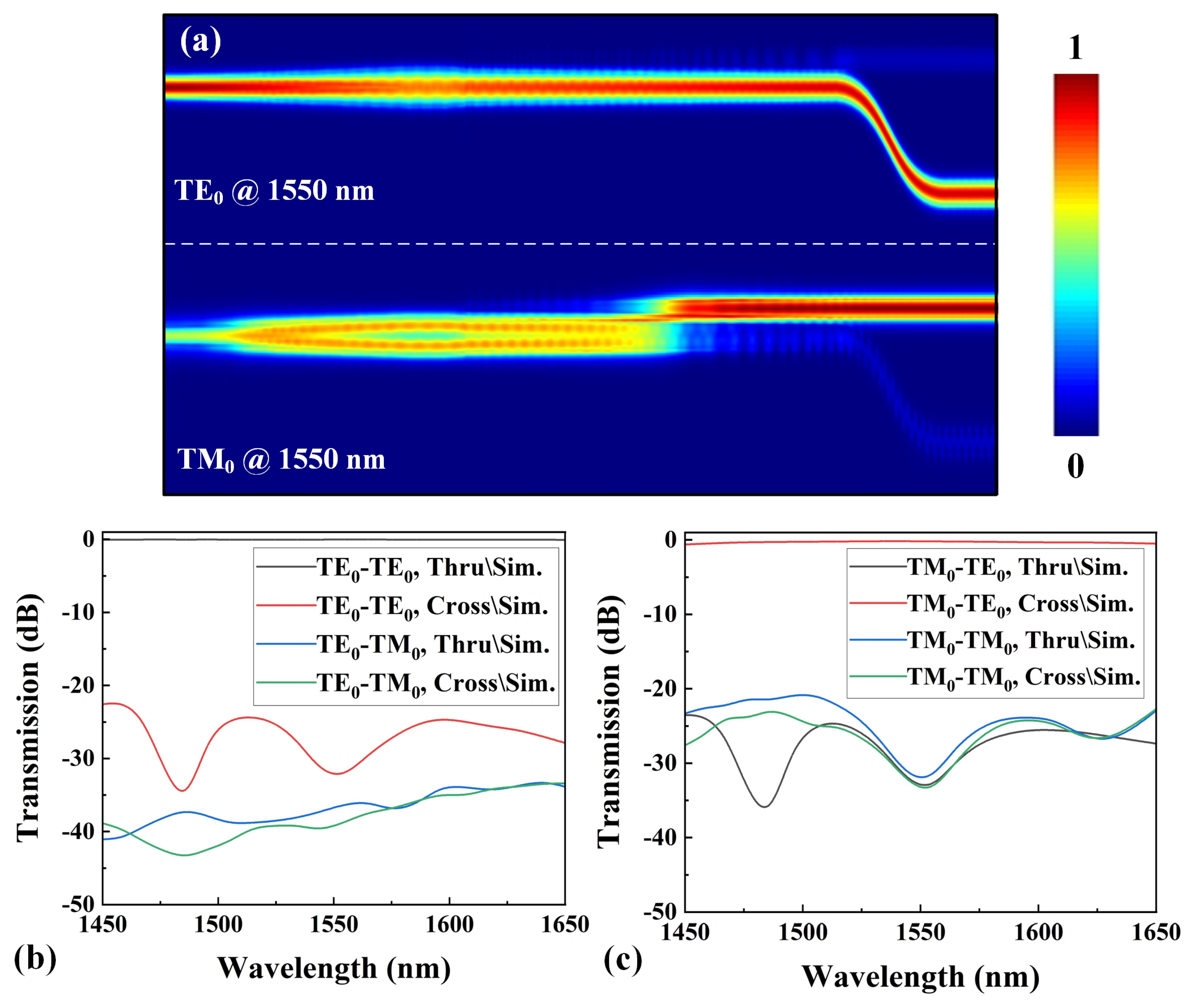
As illustrated in Figure 1a, an inverse-tapered coupler is employed as the MD which routes the TE 0 and TE 1 modes to desired output ports. The TE 0 mode would propagate through the MD without conversion and output from the through port, while the TE 1 mode would couple to TE 0 mode and output from the cross-port. The design principle of MD is similar to [20] but is applied to the waveguides with a height of 150 nm. The width of the through waveguide decreases from 0.95 μ m to 0.65 μ m, whereas the width of the cross-waveguide increases from 0.2 μ m to 0.5 μ m. The length of the taper is set as 100 μ m for the adiabatic mode evolution, and the gap between the tapers is fixed as 0.2 μ m. By connecting the APR with MD, the simulated optical power distribution in the designed PSR is shown in Figure 3a. At the wavelength of 1550 nm, the injected TE 0 mode outputs from the through port directly. Meanwhile, the TM 0 mode is converted to TE 0 mode and outputs from the cross-port. When TE 0 or TM 0 mode is injected, the transmissions of both TE 0 and TM 0 modes from the through/cross-ports are monitored and shown in Figure 3b,c, respectively. At a wavelength range of 1450 nm to 1650 nm, the insertion losses (ILs) of the desired mode are less than 1 dB for both polarizations, and the cross-talk induced by the unwanted modes are lower than −20 dB. The proposed PSR exhibits a superior performance with a broad operating wavelength covering S, C, and L bands.

3. Fabrication and Measurement

The proposed device was fabricated through a commercial MPW run (HOPHO Inc., Xingu Industrial Park, Shuangliu District, Chengdu City, China). It was processed on an SOI wafer with a 220 nm top silicon layer and a 2 μ m buried oxide layer. To define the pattern of the devices, 193 nm-deep ultraviolet (UV) photolithography was used, while inductively coupled plasma (ICP) was used to etch the silicon layers. Finally, a silica upper-cladding was deposited on the structure by a plasma-enhanced chemical vapor deposition (PECVD) process. Grating couplers (GCs) are implemented for light coupling from fibers; the periods of grating couplers for the TE and TM modes are 620 nm and 984 nm, respectively. The fill factor and etching depth of the grating couplers are 0.5 and 70 nm, respectively. Figure 4a shows the optical micrograph of the fabricated PSR; the rectangles covering the PSRs are the trenches that have no influence on the device. To fully characterize the performance, four test structures with the same geometry but different GCs are fabricated. A tunable laser (Santec TSL-550) is used as the source and an optical power meter is used to measure the optical power.
The transmission spectra of the reference grating couplers are shown in Figure 4b. The maximum coupling efficiencies of TE 0 and TM 0 grating are 5 dB/facet and 6 dB/facet, accompanied with an attenuation of around 12 dB at the long wavelengths. Limited by the tunable range of lasers and the bandwidth of GCs, the measurement is carried out within a bandwidth from 1500 nm to 1575 nm. The experimental results are shown in Figure 5 (solid curves). As a comparison, the simulation results are also attached in Figure 5 (dashed curves). We see that for TE 0 injection, the IL is less than 1 dB, and the cross-talk is below −20 dB for the whole band. For TM 0 injection, the IL increases as the wavelength rises up because the sidewall roughness of the MD induces extra propagation loss for the TE 1 mode. However, the IL for TM 0 injection is still less than 1.5 dB, while the cross-talk is kept below −20 dB over the band. However, the transmissions of the TE-TE Cross, TE-TM Thru, TE-TM Cross, TM-TE Thru, and TM-TM Thru ports are far lower than the simulation results at the long wavelength. Since the grating coupler introduces a huge power attenuation at the long wavelength, the cross-talk cannot be detected due to the limited sensitivity of the power meter. Similarly, the transmission of the TM-TM Cross-port is also out of detection for the whole band.
Table 2 shows a comparison among reported APR-based PSRs on the SOI platform. We can find that the APR of our design has an apparently compact size. Additionally, the proposed PSR exhibits a nice performance over a broad bandwidth. We note that the measured results are limited by our experimental setup. A broader operation bandwidth would probably be obtained if either the laser source is updated or the GCs are further optimized. We will make efforts to fix these problems in our future work.

4. Conclusions

We experimentally demonstrated a broadband PSR based on a bi-level taper and an inverse-tapered coupler. The device is designed with a 150 nm-high slab waveguide that suits the active silicon photonics platform. The footprint of the APR is significantly shrunken from hundreds to tens of microns while maintaining a high conversion efficiency of >95% over 1250 nm to 1650 nm. Connecting the APR with the mode splitter, the device exhibits a low loss of <1 dB and a cross-talk of <−20 dB over a broadband from 1450 nm to 1650 nm. The proposed PSR is fabricated through the commercial MPW program, and the loss of <1.5 dB and cross-talk of <−20 dB are confirmed for a bandwidth of 75 nm. This device offers a promising solution for ultra-compact PSRs and potential applications in integratable optical communication links and optical interconnection networks.

Author Contributions

Conceptualization, Y.T. and Z.K.; methodology, Y.T. and Y.L. (Yan Li); software, Y.L. (Yegang Lv); investigation, Y.T.; data curation, Y.T., T.D. and P.X.; writing—original draft preparation, Y.T.; writing—review and editing, Z.K. and X.Z.; supervision, Z.K.; project administration, X.Z.; funding acquisition, X.Z. All authors have read and agreed to the published version of the manuscript.

Funding

This work was supported by the National Nature Science Foundation of China (NSFC) (62105167, 62075188, 61974078); Natural Science Foundation of Zhejiang Province (LQ22F050008, LY21F050007, LY21F040002, LQ21F040001); Natural Science Foundation of Ningbo (2021J074, 2021J059); Key Research and Development Program of Jiangsu Province (BE2021082).

Institutional Review Board Statement

Not applicable.

Informed Consent Statement

Not applicable.

Data Availability Statement

The data presented in this study are available on request from the corresponding author. The data are not publicly available due to the data also forming part of an ongoing study.

Acknowledgments

The authors express their appreciation to the anonymous reviewers for their valuable suggestions.

Conflicts of Interest

The authors declare no conflict of interest.

References

  1. Baehr-Jones, T.; Pinguet, T.; Lo Guo-Qiang, P.; Danziger, S.; Prather, D.; Hochberg, M. Myths and rumours of silicon photonics. Nat. Photonics 2012, 6, 206–208. [Google Scholar] [CrossRef]
  2. Shi, W.; Tian, Y.; Gervais, A. Scaling capacity of fiber-optic transmission systems via silicon photonics. Nanophotonics 2020, 9, 4629–4663. [Google Scholar] [CrossRef]
  3. Tian, Y.; Qiu, J.; Liu, C.; Tian, S.; Huang, Z.; Wu, J. Compact polarization beam splitter with a high extinction ratio over S+ C+ L band. Opt. Express 2019, 27, 999–1009. [Google Scholar] [CrossRef] [PubMed]
  4. Mao, S.; Cheng, L.; Zhao, C.; Fu, H. Ultra-broadband and ultra-compact polarization beam splitter based on a tapered subwavelength-grating waveguide and slot waveguide. Opt. Express 2021, 29, 28066–28077. [Google Scholar] [CrossRef] [PubMed]
  5. Li, C.; Dai, D.; Bowers, J.E. Ultra-broadband and low-loss polarization beam splitter on silicon. In Optical Fiber Communication Conference; Optical Society of America: Washington, DC, USA, 2020; p. Th1A.4. [Google Scholar]
  6. Ao, X.; He, S. Polarization beam splitters based on a two-dimensional photonic crystal of negative refraction. Opt. Lett. 2005, 30, 2152–2154. [Google Scholar] [CrossRef] [PubMed]
  7. Wu, F.; Chen, M.; Xiao, S. Wide-angle polarization selectivity based on anomalous defect mode in photonic crystal containing hyperbolic metamaterials. Opt. Lett. 2022, 47, 2153–2156. [Google Scholar] [CrossRef] [PubMed]
  8. Shi, X.; Zhang, J.; Fan, W.; Lu, Y.; Peng, N.; Rottwitt, K.; Ou, H. Compact low-birefringence polarization beam splitter using vertical-dual-slot waveguides in silicon carbide integrated platforms. Photonics Res. 2022, 10, A8–A13. [Google Scholar] [CrossRef]
  9. Zhang, J.; Shi, X.; Zhang, Z.; Guo, K.; Yang, J. Ultra-compact, efficient and high-polarization-extinction-ratio polarization beam splitters based on photonic anisotropic metamaterials. Opt. Express 2022, 30, 538–549. [Google Scholar] [CrossRef]
  10. Yu, Z.; Xu, H.; Liu, D.; Li, H.; Shi, Y.; Dai, D. Subwavelength-Structure-Assisted Ultracompact Polarization-Handling Components on Silicon. J. Light. Technol. 2022, 40, 1784–1801. [Google Scholar] [CrossRef]
  11. Liu, C.; Qiu, J.; Tian, Y.; Guo, H.; Hong, X.; Wu, J. Performance Enhancement of a Broadband Polarization Rotator by using Modified Mode Converters. In Asia Communications and Photonics Conference; Optical Society of America: Washington, DC, USA, 2018; p. Su2A–171. [Google Scholar]
  12. Xu, H.; Shi, Y. Subwavelength-grating-assisted silicon polarization rotator covering all optical communication bands. Opt. Express 2019, 27, 5588–5597. [Google Scholar] [CrossRef]
  13. Lebbe, N.; Glière, A.; Hassan, K. High-efficiency and broadband photonic polarization rotator based on multilevel shape optimization. Opt. Lett. 2019, 44, 1960–1963. [Google Scholar] [CrossRef] [Green Version]
  14. Gallacher, K.; Griffin, P.F.; Riis, E.; Sorel, M.; Paul, D.J. Silicon nitride waveguide polarization rotator and polarization beam splitter for chip-scale atomic systems. APL Photonics 2022, 7, 046101. [Google Scholar] [CrossRef]
  15. Yan, X.; Chen, J.; Dai, D.; Shi, Y. Polarization multiplexing silicon-photonic optical phased array for 2D wide-angle optical beam steering. IEEE Photonics J. 2021, 13, 1–6. [Google Scholar] [CrossRef]
  16. Dong, P.; Chen, Y.K.; Duan, G.H.; Neilson, D.T. Silicon photonic devices and integrated circuits. Nanophotonics 2014, 3, 215–228. [Google Scholar] [CrossRef]
  17. Ma, M.; Park, A.H.; Wang, Y.; Shoman, H.; Zhang, F.; Jaeger, N.A.; Chrostowski, L. Sub-wavelength grating-assisted polarization splitter-rotators for silicon-on-insulator platforms. Opt. Express 2019, 27, 17581–17591. [Google Scholar] [CrossRef]
  18. Zhang, Y.; Zhu, Q.; He, Y.; Su, Y. Silicon polarization splitter and rotator with tolerance to width variations using a nonlinearly-tapered and partially-etched directional coupler. In Optical Fiber Communication Conference; Optical Society of America: Washington, DC, USA, 2019; p. W1E.4. [Google Scholar]
  19. Xie, C.; Zou, X.; Zou, F.; Zhang, Y. High-performance ultra-compact polarization splitter-rotators based on dual-etching and tapered asymmetrical directional coupler. Chin. Opt. Lett. 2021, 19, 121301. [Google Scholar] [CrossRef]
  20. Sacher, W.D.; Barwicz, T.; Taylor, B.J.; Poon, J.K. Polarization rotator-splitters in standard active silicon photonics platforms. Opt. Express 2014, 22, 3777–3786. [Google Scholar] [CrossRef] [Green Version]
  21. Chen, X.; Qiu, C.; Sheng, Z.; Wu, A.; Huang, H.; Zhao, Y.; Li, W.; Wang, X.; Zou, S.; Gan, F.; et al. Design of an ultra-broadband and fabrication-tolerant silicon polarization rotator splitter with SiO2 top cladding. Chin. Opt. Lett. 2016, 14, 081301–81305. [Google Scholar] [CrossRef] [Green Version]
  22. Zhao, Y.; Qiu, C.; Wu, A.; Huang, H.; Li, J.; Sheng, Z.; Li, W.; Wang, X.; Gan, F. Broadband polarization splitter-rotator and the application in WDM receiver. IEEE Photonics J. 2018, 11, 1–10. [Google Scholar] [CrossRef]
  23. El-Fiky, E.; Wang, Y.; Bernal, S.; Gamache, C.; Panorel, E.; Kumar, A.; Samani, A.; Jacques, M.; Koh, P.c.; Plant, D.V. High extinction ratio and broadband O-band polarization splitter and rotator on silicon-on-insulator. In Proceedings of the 2019 Optical Fiber Communications Conference and Exhibition (OFC), San Diego, CA, USA, 3–7 March 2019; pp. 1–3. [Google Scholar]
  24. Chen, Z.; Yang, J.; Wong, W.H.; Pun, E.Y.B.; Wang, C. Broadband adiabatic polarization rotator-splitter based on a lithium niobate on insulator platform. Photonics Res. 2021, 9, 2319–2324. [Google Scholar] [CrossRef]
  25. Sun, C.; Yu, Y.; Chen, G.; Zhang, X. A low crosstalk and broadband polarization rotator and splitter based on adiabatic couplers. IEEE Photonics Technol. Lett. 2016, 28, 2253–2256. [Google Scholar] [CrossRef]
  26. Rostamian, A.; Guo, J.; Chakravarty, S.; Yan, H.; Chung, C.J.; Heidari, E.; Chen, R.T. Grating-coupled silicon-on-sapphire polarization rotator operating at mid-infrared wavelengths. IEEE Photonics Technol. Lett. 2019, 31, 401–404. [Google Scholar] [CrossRef]
  27. Chen, D.; Liu, M.; Zhang, Y.; Wang, L.; Hu, X.; Feng, P.; Xiao, X.; Yu, S. C+ L band polarization rotator-splitter based on a compact S-bend waveguide mode demultiplexer. Opt. Express 2021, 29, 10949–10957. [Google Scholar] [CrossRef]
  28. Dai, D.; Wu, H. Realization of a compact polarization splitter-rotator on silicon. Opt. Lett. 2016, 41, 2346–2349. [Google Scholar] [CrossRef]
  29. Guo, D.; Chu, T. Broadband and low-crosstalk polarization splitter-rotator with optimized tapers. OSA Contin. 2018, 1, 841–850. [Google Scholar] [CrossRef]
  30. Available online: http://www.hopho.com.cn/khdzfw/31.html (accessed on 6 October 2022).
  31. Dai, D.; Tang, Y.; Bowers, J.E. Mode conversion in tapered submicron silicon ridge optical waveguides. Opt. Express 2012, 20, 13425–13439. [Google Scholar] [CrossRef]
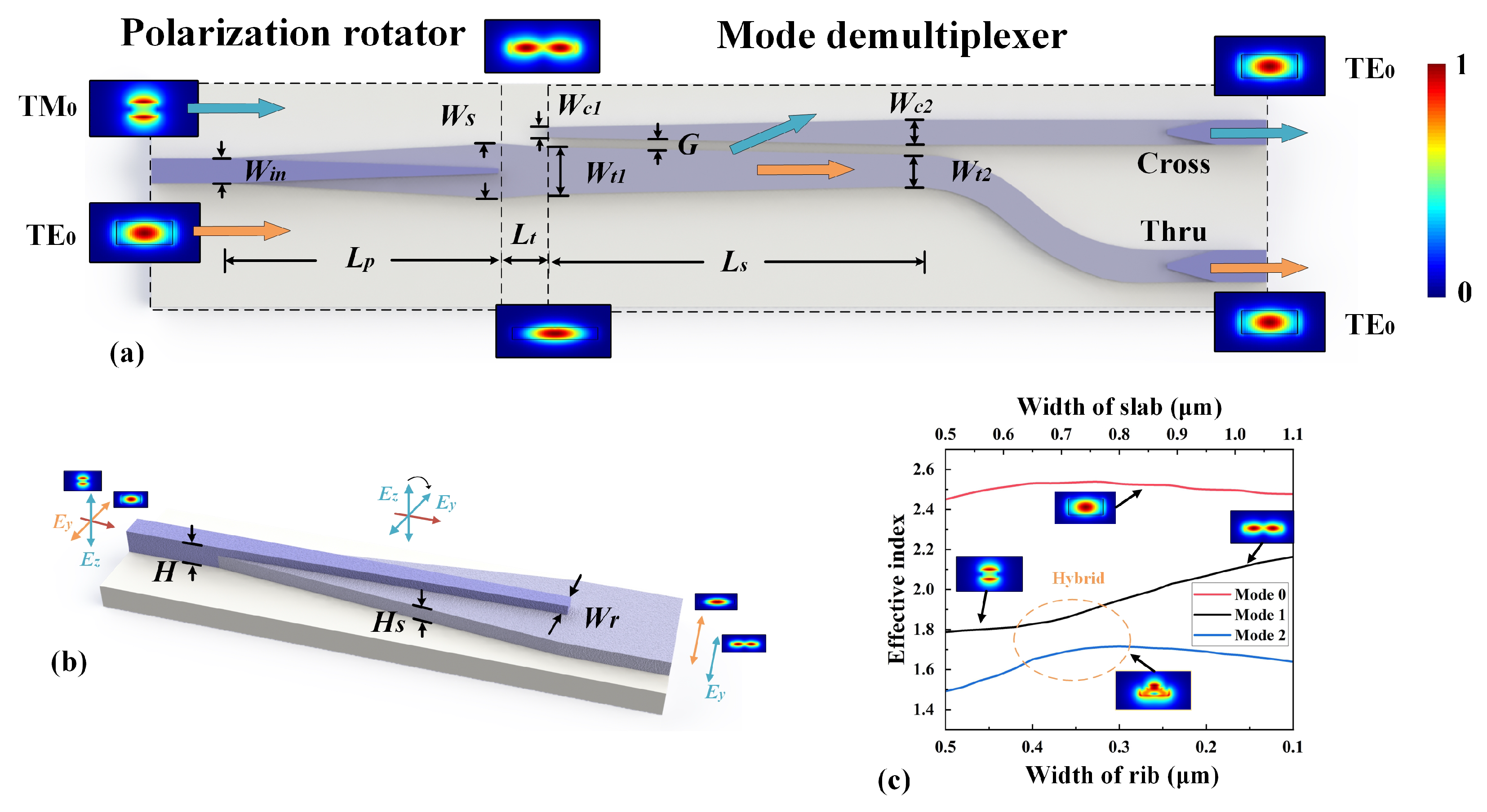
Figure 1. (a) The schematic diagram of the proposed PSR. (b) The 3D schematic diagram of the APR. (c) The calculated effective refractive indices of the first three modes as a function of the width variation for both slab and rib waveguides.
Photonics 09 00758 g001
Figure 2. (a) Calculated conversion efficiency over a bandwidth of 1250–1650 nm for different lengths from 20 μ m to 70 μ m. (b) Optical power distribution and the modal field evolution along the propagation axis of the APR at the wavelengths of 1250 nm, 1450 nm, and 1650 nm.
Photonics 09 00758 g002
Figure 3. (a) Simulated optical power distribution along the designed PSR in case of TE 0 or TM 0 injection. Transmission spectrum for (b) TE 0 injection and (c) TM 0 injection.
Photonics 09 00758 g003
Figure 4. (a) Optical micrograph of the fabricated devices. (b) Transmission responses of the reference grating couplers.
Photonics 09 00758 g004
Figure 5. Measured transmission spectra for the (a) TE 0 and (b) TM 0 injection.
Photonics 09 00758 g005
Table 1. Parameters and values of the PSR.
ParametersValues ( μ m)ParametersValues ( μ m)
W i n 0.5 W t 1 0.95
W r 0.1 W t 2 0.65
W s 1.1 W c 1 0.2
L t 5 W c 2 0.5
L s 100H0.22
G0.2 H s 0.15
Table 2. Performance comparison of APR-based PSRs on the SOI platform.
ReferenceAPR Length ( μ m)IL (dB)Cross-Talk (dB)Bandwidth (nm)Etching Depth (nm)Exp./Sim.
[20]1001.6−1350220/130Experiment
[21]53.50.2−15320220/130Simulation
[22]53.50.73−12.1110220/130Experiment
[25]701−14100220/130Experiment
[27]1000.6−17.6110220/70Experiment
This work301−20200220/70Simulation
This work301.5−2075220/70Experiment
Publisher’s Note: MDPI stays neutral with regard to jurisdictional claims in published maps and institutional affiliations.