Article

Theoretical Analysis of Optical Properties for Amorphous Silicon Solar Cells with Adding Anti-Reflective Coating Photonic Crystals

by
Hassan Sayed
1,
Mawaheb Al-Dossari
2,
Mohamed A. Ismail
3,4,
Nashaat S. Abd El-Gawaad
5 and
Arafa H. Aly
1,*
1
TH-PPM Group, Physics Department, Faculty of Sciences, Beni-Suef University, Beni-Suef 62511, Egypt
2
Department of Physics, Faculty of Science, King Khalid University, Abha 62529, Saudi Arabia
3
Faculty of Technology and Education, Beni-Suef University, Beni Suef 62521, Egypt
4
Physics Department, University College in Al-Aarda, Jazan University, Jazan 82817, Saudi Arabia
5
Faculty of Sciences, King Khalid University, Mohayel Asser, Abha 61421, Saudi Arabia
*
Author to whom correspondence should be addressed.
Photonics 2022, 9(11), 813; https://doi.org/10.3390/photonics9110813
Submission received: 19 September 2022 / Revised: 19 October 2022 / Accepted: 20 October 2022 / Published: 28 October 2022
(This article belongs to the Special Issue Recent Progress in Solar Cell Technology and Future Prospects)

Abstract

:
In the current study, we aim to limit the power dissipation in amorphous silicon solar cells by enhancing the cell absorbance at different incident angles. The current improvement is justified by adding the single-period of ternary 1D photonic crystal with texturing on the top surface, which acts as an anti-reflecting coating. The texturing shape gives the photons at least two chances to localize inside the active area of the cell. Therefore, it increases the absorbance of the cell. Moreover, we add binary one-dimensional photonic crystals with the features of a photonic band gap, which acts as a back mirror to return the photons that were transmitted inside the cell’s active region. The considered structure is demonstrated by the well-defined finite element method (FEM) by using COMSOL multiphysics.

1. Introduction

The photovoltaic effect is the conversion of light into energy by a solar cell, which is a two-terminal semiconducting device. Despite the fact that the phenomena has been known for more than a century [1], its uses and influence remained limited due to its initial high cost when compared to other alternatives such as oil and nuclear power plants. In 1954, Chapin et al. built the first solar cells with a six percent efficiency using crystalline silicon technology [2]. Since then, Si technology has been regarded as the PV market’s black horse [3,4,5,6]. Furthermore, Si-based PV technology accounts for between 80% and 90% of the market; however, it is anticipated that c-Si PV panels’ market share will decline from 92% in 2014 to 44.8% in 2030 [7]. The low efficiency of silicon solar cells pushed researchers to limit power dissipation by using an artificial material, which is known as photonic crystal (PCs) [8].
PCs are artificially created inhomogeneous structures with periodic changes in refractive indices in one dimension and a homogeneous in the other two dimensions, and are classified as 1D-PCs, 2D-PCs, and 3D-PCs [9,10,11,12]. PCs alter the propagation of incident electromagnetic waves in several ways [13,14]. The use of 1D-PCs is widespread in several applications owing to its low cost, ease of fabrication, and high control of the electromagnetic wave localization. Therefore, it is used in water desalination [15], wave guides, sensors [16,17], and advanced optical devices. Additionally, 1D-PCs can be essential for improving solar cell efficiency [18,19].
Numerous PC topologies were demonstrated as a result, with the aim of decreasing the reflectance of a silicon surface for solar cell applications [20,21]. Recently, researchers and scientists devoted their efforts to limiting the power dissipation in silicon solar cells to enhance the conversion efficiency by using photonic crystals [22,23,24]. Due to the high contrast between silicon and air, most of the incident electromagnetic waves are reflected from the silicon’s top surface, wherein the reflectivity of amorphous silicon reaches 35%, as reported by Sprafke et al. [25]. Additionally, without any anti-reflection coating, the National Renewable Energy Center (CENER) used a chemical approach to alter the surface morphology of amorphous silicon that is texturized with inverted pyramids: the reflectivity is increased to 16%, as demonstrated by Anderson et al. [26].
Furthermore, surface texturing for thin-film silicon solar cells was a focus of research in recent decades [27]. Therefore, the structure of PCs is immersed between air and the silicon cell as an anti-reflection coating (ARC) to degrade the refractive index and increase the absorbance of the cell.
For a more practical procedure, physical vapor oblique angle deposition (PV-OAD) in an electron bombardment evaporator reactor could be used to create the 1D-PCs at room temperature [28,29,30]. The thicknesses of layers are regulated by adjusting the evaporation rate, which ranges from 1 to 1.5 (Å·S−1). ITO glass and a Si (100) wafer are both flat substrates that are positioned at a zenithal evaporation angle (α) of 70° in relation to the evaporation source. In order to construct the structure with a texturing morphology, the substrate is rotated by 180 degrees around the azimuthal axis (ϕ) every 500 nm until the required thickness is reached. The multilayer structure is then deposited under similar circumstances. Between each layer, the substrate is additionally azimuthally rotated by 180 degrees [31].
The goal of this research is to develop simple and efficient structures for each anti- reflection coating (ARC) and back reflector that improves the optical characteristics of a-si solar cells. To begin, ARC structures are made up of texturing ternary 1D-PCs for one period, as the texturing shape gives the photons at least two chances to localize inside the active area of the cell. Moreover, texturing surfaces increase the absorbance at different incident angles in contrast to planner ternary PCs. Then, we design 1D-PCs with the concept of photonic band gap (PBG) to deal with the leakage photons within the electronic energy gap of the hydrogenated amorphous silicon solar cell ( E g = 1.7   ev ) , which represents the photons from 350 nm to 730 nm. In Section 2, we provide a basic review of theoretical modelling. The numerical results and conclusions are then explained separately.

2. Modeling and Simulation

In this part, we are concerned with the designed structure to trap all of the incident electromagnetic waves in the visible spectrum to generate electron–hole pairs to produce electricity. Firstly, we study the fundamental concepts of the geometry of the structure and its effect on light trapping. Then, we show a brief theoretical and simulation model with the COMSOL multiphysics program, which is based on the fundamentals of the finite element method (FEM). Here, Figure 1 represents the considered structure of the hydrogenated amorphous silicon (H: a-Si) solar cell with a modification in each anti-reflection coating and back reflector. Also, in Figure 2, we illustrate the path of the photon inside the texturing surface to localize in the active area of the cell, wherein the shape of the pyramid gives the photons at least two chances to localize on the active layer of the cell. Therefore, the absorption characteristics of the solar cell in the presence of an anti-reflective coating on the cell’s top surface could be investigated using wave optics and semiconductor modules, which is expected to decrease the reflectivity and increase the absorbance of the cell as in Equation (1) [32,33].
A λ = 1 T λ R λ
where T λ ,   and   R λ are the transmittance and reflectance as a function of incident wavelength, respectively. Additionally, it is necessary to solve the Poisson (Equation (2)) and continuity (Equations (3) and (4)) equations in order to estimate the electrostatic potential, electron concentration n (cm−3), and hole concentration p (cm−3) as functions of space [33,34].
· ε s ϕ = ρ
n t 1 q · J n + U n = 0
p t 1 q · J h + U h = 0
where ε s and ρ are the semiconductor permittivity and space charge density, respectively, q is the electron charge, ( J n ,   J h ) are current densities [A/ cm 2 ] , and U n ,   U h are the net number of electrons and holes recombined in the unit of time and volume [1/ S · cm 3 ].
P = q n p + N A N D
U n = R n G n
U h = R h G h  
where G n ,   R n are the generation and the recombination rates of electrons where in,   G h ,   R h are generation and recombination rate of holes, respectively. The active area of the cell consists of the p-region, intrinsic region, and n-region, with thicknesses of 15 nm, 200 nm, and 27 nm, respectively. As seen in Figure 1, this disintegrates into a silicon wafer.
For the simulation procedure, the meshing size must be 10 times smaller than the smallest incident wavelength, in order to obtain more accurate results in the finite element method, as we discuss in our previous work [19]. The simulation meshing parameters are the maximum element size equal to 3 × 10 9   m , minimum element size equal to 1.51 × 10 10   m , and the maximum element growth rate is 1.3.

3. Results and Discussion

Our results and discussions are displayed through three stages; firstly, we show the effect of inserting an anti-reflection coating above the upper surface of amorphous silicon solar cells on the absorbance of the cell by reducing the amount of reflected spectrum. Then, in the second stage, we show the optical properties of the one-dimensional photonic crystals that act as a back reflector to the cell. Finally, we show the absorbance of the cell with each anti-reflection coating and back reflector by changing the incident angle. We also compute the optical generation of electron–hole pairs, which indicates the overall efficiency of the cell.

3.1. Anti-Reflection Coating

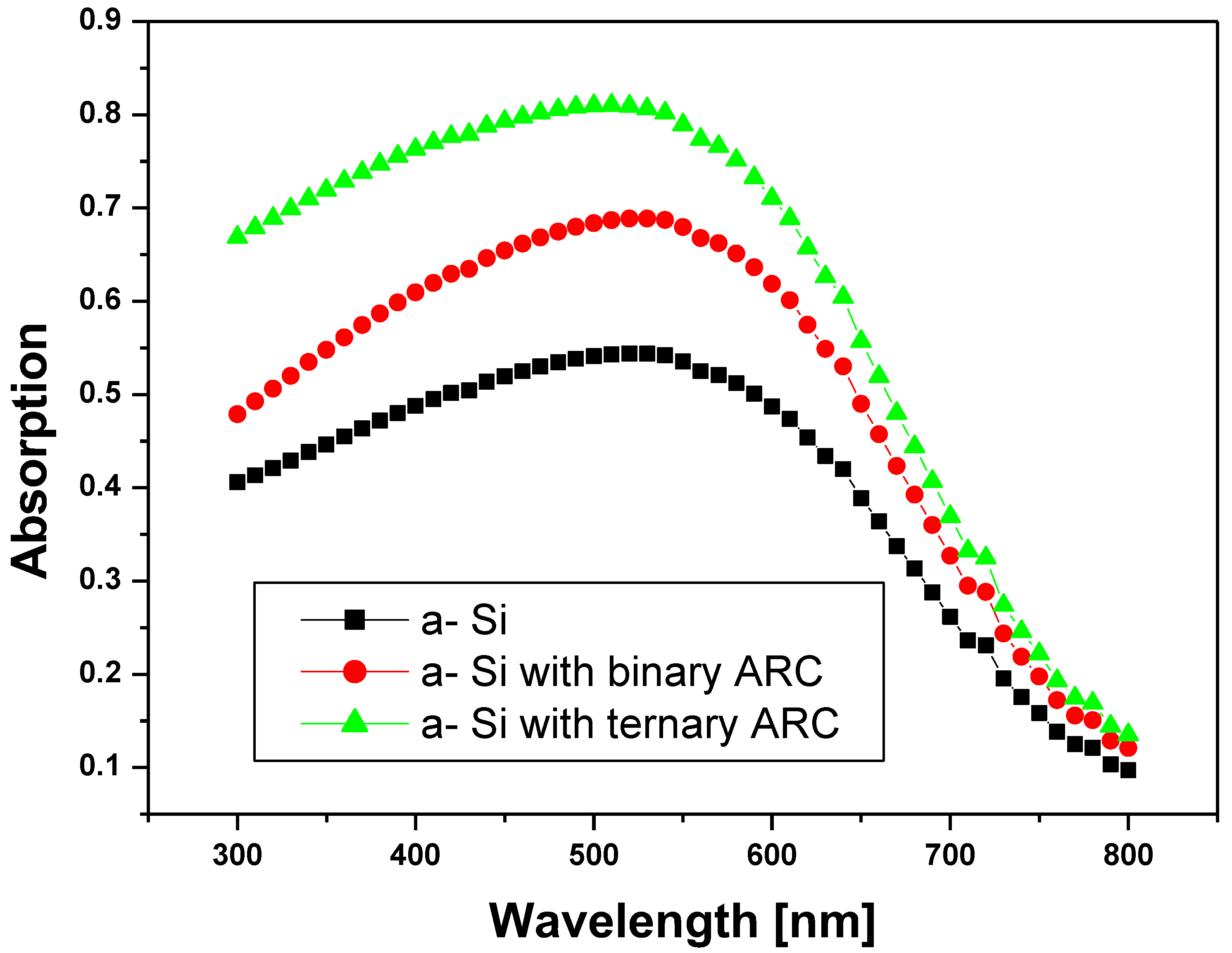
We design step-index structures to reduce the dielectric contrast between the air and amorphous silicon to reduce the reflection spectrum. Here, in Figure 3, we compare 1D binary PCs and ternary PCs in reaching low reflectivity at normal incidence. The binary ARC is composed of   A B N ; the A layer is silicon dioxide   S i O 2 , with thickness d 1 = 54   nm and refractive index n 1 = 1.46 [35], the B layer is titanium dioxide T i O 2 with d 2 = 82   nm and n 2 = 2.5 [36], and N equal one period. Also, the ternary ARC is composed of A C B N ; the A layer is S i O 2 with d 1 = 54   nm and n 1 = 1.46 ; the C layer is silicon nitride S i 3 N 4 with d 2 = 33   nm and n 2 = 2.0167 [37]; the B layer is T i O 2 with d 3 = 82   nm and n 3 = 2.5 , and N equal one period.
Here, we find in the case of 1D ternary PCs, the absorption reaches 80% at an incident wavelength equal to 500 nm, which is higher than the others. Due to the ternary structure, we verify the step-index as the following equation.
n a i r < n S i O 2 < n S i 3 N 4 < n T i O 2 < n a S i
Therefore, increasing the number of layers with step-index between the air and amorphous silicon causes enhancement of the cell absorbance, as shown in Figure 3. However, we still have an effective amount of reflective spectrum. Thus, we texture the top surface of the anti-reflection coating, as the texturing surface give the photons at least two chances to localize inside the cell, as we discussed previously in Section 2.
In Figure 4, we show the absorbance of amorphous silicon solar cells with the optimized ternary PCs as in Figure 3, and ternary PCs with added texturing from silicon dioxide on the surface with different heights of the texturing. Here, with height h = 25   nm , the absorbance A = 87 % is enhanced with respect to the ternary planner A = 80 % at incident wave λ = 500   nm as shown; also, the result for h = 50   nm is approximately the same as h = 25   nm . However, by increasing the height to 100 nm, the absorbance is decreased as A = 77 % at the same incident wavelength. In addition, the absorbance is not affected by changing the width of the texturing. All the last results are at the normal incidence. Therefore, we must study the effect of the incident angle on the cell absorbance, as in the following Section 3.2.

3.2. Back Reflector

In the subsection, before we design the back reflector, we must calculate the reflected and transmitted spectrum from the cell with ARC to determine the effective range of the designed back reflector. Thus, Figure 5 shows the reflected and transmitted spectrum from the modified cell in the last subsection by adding the ARC optimum structure. Here, we find that the reflectivity is very small as to the effect of adding ARC. We also find that the photons from 550 nm to 730 nm are transmitted from the cell with a remarkable ratio, as shown. Therefore, we design one-dimensional binary photonic crystals to create a photonic band gap in the range of the transmitted photons from 550 nm to 730 nm. The binary back reflector is composed of A B N , the A layer is silicon dioxide S i O 2 , with thickness d 1 = 40   nm and refractive index n 1 = 1.46 [32], the B layer is silicon S i with d 2 = 75   nm and n 2 = 3.3 [38,39], and the number of periods (N) equal to 12 periods, as shown in Figure 6.
In Figure 6, we find that the considered structure allows wavelengths between 350 and 550 nanometers to be transmitted through it, as shown in the p-color figure. It completely blocks the photons in the wavelengths from 550 nm to 750 nm, as in p-color, which is considered the photonic band gap of the structure, and this is very suitable for our modified amorphous silicon cell. Therefore, we add the last structure as a back reflector of our structure of amorphous silicon with a texturing anti-reflection coating.

3.3. The Optical Properties of the Cell

In this subsection, we study the optical properties of amorphous silicon solar cells with each textured anti-reflection coating and one-dimensional photonic crystals as a back reflector. In addition, we study the effect of incident angle in the environment of the cell to show the best structure for the cell with high efficiency. Finally, we calculate the optical generation rate of electron–hole pairs in the active area of the cell.
In Figure 7, we notice that the absorbance is enhanced by adding a back reflector in the range of photonic bandgap, as in Figure 6. That is why the back reflector reflects the transmitted photons to localize in the active area, which increases the absorbance of the cell. These are the last results are at the normal incidence, therefore, we study the effect of the incident angle to choose the best structure, as the incident angle is varying during the hours of the day.
In Figure 8, we study the absorbance of the cell at the oblique incident for planner ternary ARC and textured surfaces with different heights (25 nm and 50 nm). The absorbance is decreased by increasing the incident angle for all different structures of ARC, and the difference between the absorbance of the three structures is increased by increasing the incident angle. The best structure for all incident angles is the texturing surface with a height equal to 50 nm, as shown. Therefore, we show in Figure 9 the absorbance of the cell with texturing ARC when the height of the pyramids equals 50 nm. Here, we notice that the absorbance is increased by increasing the incident angle from normal incidence to oblique incidence with an angle of 40 degrees. Also, at an incident angle equal 50 degrees, the absorbance begins to decrease with respect to the normal incident. As a result of its high absorbance at the oblique incident, this structure is more compatible with the environmental silicon solar cell. Thus, the average absorption for our optimized structure in the visible spectrum is approximately 95%, which means the average reflection is only about 5% without no transmission photons. To highlight the inspiration and innovation of our work, we added Table 1 to compare our current work to the earlier works in the literature review. Hence, we calculate the optical generation rate of this structure to be sure that the absorbed photons are assisting in the generation of electron–hole pairs as shown in Figure 10.
Finally, we can conclude from the results that changing the surface morphology of the solar cell has a significant effect on overall efficiency, and it increases efficiency at the oblique incidence in comparison to flat surfaces. Texturing and concave surfaces of the solar cell are a promising solution to overcome the low efficiency of the commercial cells.
Hence, as we optimize the optical properties of the active area of the cell and the ARC structure, we add the two contacts for our structure to be more compatible with the experimental data. Figure 11 represents the schematic structure of the cell with the two electrodes. From the dispersion relation of indium–tin–oxide (ITO) as shown in Figure 12 [43,44], we notice that the extinction coefficient is very low, so it does not affect the incident photons on the active area of the cell when we add it on the interface between the top surface of amorphous silicon and the lower surface of the designed ARC. The refractive index of ITO is approximately similar to the refractive index of O 2   n 3 = 2.5 . As a result, we can replace the layer of T i O 2 in the ARC structure with ITO, as shown in Figure 11, to serve as the front contact electrode. Also, we add a 50 nm molybdenum (Mo) electrode to act as a back contact electrode [45].
Here, in Figure 13 we study the optical properties of the considered structure in Figure 11 and compare them with the optical properties of the cell as in Figure 9 in the case of normal incidence. By adding the two electrodes, the absorption of the cell is increasing at the smaller wavelengths, and this adding causes a small difference between the optical properties with and without the two electrodes, as we show in Figure 13. Thus, our structure is compatible with the experimental date. At the same time, the ITO layer is acting as a grading index and a front electrode for the cell. Therefore, our modified structure of the textured ARC is an optimum energy-harvesting solar cell.

4. Conclusions

At the end of this study, we find that grading refractive index for an anti-reflection coating structure achieves high absorbance for the normal incidence. However, it loses this advantage for the oblique incident. Then, adding texturing to the upper surface of the grating refractive index ARC enhances the absorbance owing to the pyramid structure, giving the incident photons at least two chances to localize inside the active area of the cell. Therefore, the texturing surface is a highly trapping structure for all-optical devices, with high efficiency owing to its good ability to trap light in normal and oblique incidences. Moreover, we added one-dimensional binary PCs as back reflectors to reflect the transmitted photons [from 550 nm to 730 nm] within the range of the energy gap of the cell. Finally, by adding texturing ARC and binary one-dimensional PCs back reflectors, the absorbance is increased to 97% for the incident angle equal to 30 degrees over a wide range of the visible spectrum. We also calculated the electron–hole pair generation at different incident angles in the presence of a texturing anti-reflecting coating with a height equal to 50 nm and a back reflector. Specifically, when compared to normal incidence, the optical generation is greatly improved by the oblique incidence of the interacting radiation. Thus, for silicon solar cells, the presence of a texturing anti-reflecting coating with a height equal to 50 nm is the most compatible design for catching the majority of incident photons and enhancing cell absorption.

Author Contributions

Data curation, H.S.; M.A.-D., M.A.I. and N.S.A.E.-G.; formal analysis, N.S.A.E.-G.; funding acquisition, M.A.-D. and M.A.I.; investigation, H.S. and A.H.A.; methodology, H.S.; software, H.S.; supervision, A.H.A.; writing—original draft, H.S.; writing—review and editing, A.H.A. All authors have read and agreed to the published version of the manuscript.

Funding

This research received no external funding.

Institutional Review Board Statement

Not applicable.

Informed Consent Statement

Not applicable.

Data Availability Statement

The data that support the findings of this study are available from the corresponding author upon reasonable request.

Acknowledgments

The authors extend their appreciation to the Deanship of Scientific Research at King Khalid University for funding this work through large Groups Project under grant number RGP. 2/38/43.

Conflicts of Interest

The authors declare no conflict of interest.

References

  1. Alharbi, F.H.; Kais, S. Theoretical limits of photovoltaic efficiency and possible improvements by intuitive approaches learned from photosynthesis and quantum coherence. Renew. Sustain. Energy Rev. 2015, 43, 1073–1089. [Google Scholar] [CrossRef] [Green Version]
  2. Green, M.A. Crystalline Silicon Solar Cells. In Series on Photoconversion of Solar Energy—Clean Electricity from Photovoltaics; World Scientific: Singapore, 2015. [Google Scholar] [CrossRef] [Green Version]
  3. Healy, S.A.; Green, M.A. Efficiency enhancements in c-Si solar cells by the incorporation of a region alloyed with germanium. Sol. Energy Mat. Sol. Cells 1992, 28, 273–284. [Google Scholar] [CrossRef]
  4. Janoch, R.; Wallace, R.; Hanoka, J.I. Commercialization of Silicon Sheet via the String Ribbon Crystal Growth Technique. In Proceedings of the Conference Record of the IEEE Photovoltaic Specialists Conference, Anaheim, CA, USA, 29 September–3 October 1997; IEEE Press: Piscataway, NJ, USA, 1997; pp. 95–98. [Google Scholar]
  5. Jordan, D.; Nagle, J.P. New generation of high-efficiency solar cells: Development, processing and marketing. Prog. Photovolt. 1994, 2, 171–176. [Google Scholar] [CrossRef]
  6. Keevers, M.J.; Green, M.A. Efficiency improvements of silicon solar cells by the impurity photovoltaic effect. J. Appl. Phys. 1994, 75, 4022–4033. [Google Scholar] [CrossRef]
  7. Chowdhury, M.S.; Rahman, K.S.; Chowdhury, T.; Nuthammachot, N.; Techato, K.; Akhtaruzzaman, M.; Tiong, S.K.; Sopian, K.; Amin, N. An overview of solar photovoltaic panels’ end-of-life material recycling. Energy Strategy Rev. 2020, 27, 100431. [Google Scholar] [CrossRef]
  8. Joannopoulos, J.D.; Johnson, S.G.; Winn, J.N.; Meade, R.D. Photonic Crystals: Molding the Flow of Light; Princeton University Press: Princeton, NJ, USA, 1995. [Google Scholar]
  9. Sreekanth, K.V.; Zeng, S.; Yong, K.T.; Yu, T. Sensitivity enhanced biosensor using rapheme-based one-dimensional photonic crystal. Sens. Actuators B Chem. 2013, 182, 424–428. [Google Scholar] [CrossRef]
  10. Aly, A.H.; Mohamed, D. BSCCO/SrTiO3 One Dimensional Superconducting Photonic Crystal for Many Applications. J. Supercond. Nov. Magn. 2015, 28, 1699–1703. [Google Scholar] [CrossRef]
  11. Qing, X.; Sani, M.H. Optical refractive index sensor for detection of N2, He and CO2 gases based on square resonance nanocavity in 2D photonic crystal. Opt. Commun. 2021, 490, 126940. [Google Scholar] [CrossRef]
  12. Aly, A.H.; Ryu, S.W.; Hsu, H.T.; Wu, C.J. THz transmittance in one-dimensional superconducting nanomaterial-dielectric superlattice. Mater. Chem. Phys. 2009, 113, 382–384. [Google Scholar] [CrossRef]
  13. Al-Dossari, M.; Zaky, A.Z.; Matar, Z.S.; Aly, A.H. Effect of geometrical and physical properties of cantor structure for gas sensing applications. Accept. Synth. Met. 2022, 291, 117167. [Google Scholar]
  14. Yablonovitch, E. Inhibited spontaneous emission in solid-state physics and electronics. Phys. Rev. Lett. 1987, 58, 2059–2062. [Google Scholar] [CrossRef] [PubMed] [Green Version]
  15. Sayed, H.; Krauss, T.F.; Aly, A.H. Versatile photonic band gap materials for water desalination. Opt.—Int. J. Light Electron Opt. 2020, 219, 165160. [Google Scholar] [CrossRef]
  16. Sayed, H.; Aly, A.H. Salinity optical sensor by using two-dimensional photonic crystals: Computational study. Mater. Sci. Eng. B 2021, 269, 115169. [Google Scholar] [CrossRef]
  17. Sayed, H.; Alamri, S.; Matar, Z.; Aly, A.H. Salinity sensor based on 1D photonic crystals by Tamm resonance with different geometrical shapes. Plasmonic 2021, 17, 409–422. [Google Scholar] [CrossRef]
  18. Aly, A.H.; Sayed, H. Computer simulation and modeling of solar energy based on photonic band gap materials. Opt. Appl. 2018, 48, 117–126. [Google Scholar]
  19. Aly, A.H.; Sayed, H. Enhancement of the solar cell based on nanophotonic crystals. J. Nanophotonics 2017, 11, 046020-9. [Google Scholar] [CrossRef]
  20. Aly, A.H.; Sayed, H. Photonic band gap materials and monolayer Solar cell. Surf. Rev. Lett. 2018, 25, 1850103-6. [Google Scholar] [CrossRef]
  21. Taha, T.A.; Sayed, H.; Aly, A.H.; Elsayed, H.A. Textured concave anti-reflecting coating and convex back reflector to enhance the absorbance of amorphous Si solar cells. Phys. Scr. 2022, 97, 055503. [Google Scholar] [CrossRef]
  22. Kuang, P.; Eyderman, S.; Hsieh, M.L.; Post, A.; John, S.; Lin, S.Y. Achieving an accurate surface profile of a photonic crystal for near-unity solar absorption in a super thin film architecture. ACS Nano 2016, 10, 616–621. [Google Scholar] [CrossRef]
  23. Lin, Y.Y.; Xu, Z.; Yu, D.L.; Lu, L.F.; Yin, M.; Tavakoli, M.M.; Chen, X.Y.; Hao, Y.Y.; Fan, Z.Y.; Cui, Y.X.; et al. Dual-layer nanostructured flexible thin-film amorphous silicon solar cells with enhanced light harvesting and photoelectric conversion efficiency. ACS Appl. Mater. Interfaces 2016, 8, 10929–10936. [Google Scholar] [CrossRef]
  24. Sai, H.; Matsui, T.; Saito, K.; Kondo, M.; Yoshida, I. Photocurrent enhancement in thin film silicon solar cells by combination of anti-reflective sub-wavelength structures and light-trapping textures. Prog. Photovolt. 2015, 23, 1572–1580. [Google Scholar] [CrossRef]
  25. Sprafke, A.N.; Wehrspohn, R.B. Light trapping concepts for photon management in solar cells. Green 2012, 2, 177–187. [Google Scholar] [CrossRef]
  26. Anderson, M.J.; Whitcomb, P.J. Design of Experiments. In Kirk-Othmer Encyclopedia of Chemical Technology; John Wiley & Sons Inc.: Hoboken, NJ, USA, 2000. [Google Scholar]
  27. Yang, L.; Liu, Y.; Wang, Y.; Chena, W.; Chen, Q.; Wu, J.; Kuznetsov, A.; Du, X. 18.87%-efficient inverted pyramid structured silicon solar cell by one-step Cu-assisted texturization technique. Sol. Energy Mater. Sol. Cells 2017, 166, 121–126. [Google Scholar] [CrossRef] [Green Version]
  28. Barranco, A.; Borras, A.; Gonzalez-Elipe, A.R.; Palmero, A. Perspectives on oblique angle deposition for thin films: From fundamentasl to devices. Prog. Mater. Sci. 2015, 76, 59–153. [Google Scholar] [CrossRef] [Green Version]
  29. Hawkeye, M.M.; Brett, M.J. Glancing angle deposition: Fabrication, properties, and applications of microand nanostructured thin films. J. Vac. Sci. Technol. A 2007, 25, 1317–1335. [Google Scholar] [CrossRef]
  30. González-García, L.; Barranco, A.; Páez, A.M.; González-Elipe, A.R.; García-Gutiérrez, M.C.; Hernández, J.J.; Rueda, D.R.; Ezquerra, T.A.; Babonneau, D. Structure of glancing incidence deposited TiO(2) thin films as revealed by grazing incidence small-angle X-ray scattering. Chem. Phys. Chem. 2010, 11, 2205–2208. [Google Scholar] [CrossRef] [PubMed] [Green Version]
  31. González-García, L.; Colodrero, S.; Míguez, H.; González-Elipe, A.R. Single-step fabrication process of 1-D photonic crystals coupled to nanocolumnar TiO2 layers to improve DSC efficiency. Opt. Express 2015, 23, A1642–A1650. [Google Scholar] [CrossRef]
  32. Elliot, R.J.; Gibson, A.F. An Introduction to Solid State Physics and Its Application; William Clowes: London, UK, 1974. [Google Scholar]
  33. Tajik, J.M. Analytical and Numerical Modeling of Organic Photovoltaic Devices. Master’s Thesis, McMaster University, Hamilton, ON, Canada, 2010. [Google Scholar]
  34. Elsayed, H.A.; Sayed, H.; Taha, T.A.; Alharbi, A.G.; Alenad, A.M.; Alshammari, B.A.; Ahmed, A.M.; Mehaney, A.; Aly, A.H. Simple and efficient design towards a significant improvement of the optical absorption of amorphous silicon solar cell. J. Quant. Spectrosc. Radiat. Transf. 2021, 275, 107890. [Google Scholar] [CrossRef]
  35. Malitson, I.H. Interspecimen comparison of the refractive index of fused silica. J. Opt. Soc. Am. 1965, 55, 1205–1208. [Google Scholar] [CrossRef]
  36. Bodurov, I.; Vlaeva, I.; Viraneva, A.; Yovcheva, T.; Sainov, S. Modified design of a laser refractometer. Nanosci. Nanotechnol. 2016, 16, 31–33. [Google Scholar]
  37. Philip, H.R. Optical properties of silicon nitride. J. Electrochim. Soc. 1973, 120, 295–300. [Google Scholar] [CrossRef]
  38. Tang, J.F.; Zheng, Q. Applied Film Optics; Shanghai Science and Technology Press: Shanghai, China, 1980. [Google Scholar]
  39. Ping, L.G.; YiMin, X.; YuGe, H.; Qiang, L. Investigation of one-dimensional Si/SiO2 photonic crystals for thermo photovoltaic filter. Sci. China Ser. E Technol. Sci. 2008, 51, 2031–2039. [Google Scholar]
  40. Domínguez, S.; García, O.; Ezquer, M.; Rodríguez, M.J.; Lagunas, A.R.; Pérez-Conde, J.; Bravo, J. Optimization of 1D photonic crystals to minimize the reflectance of silicon solar cells. Photonics Nanostruct.—Fundam. Appl. 2012, 10, 46–53. [Google Scholar] [CrossRef]
  41. Zhu, J.; Yu, Z.; Fan, S.; Cui, Y. Nanostructured photon management for high performance solar cells. Mater. Sci. Eng. R Rep. 2010, 70, 330–340. [Google Scholar] [CrossRef]
  42. Zaidi, S.H.; Gee, J.M.; Ruby, D.S. Diffraction Grating Structures in Solar Cells. In Proceedings of the Conference Record of the Twenty-Eighth IEEE Photovoltaic Specialists Conference—2000 (Cat. No.00CH37036), Anchorage, AK, USA, 15–22 September 2000; pp. 395–398. [Google Scholar]
  43. Jahng, W.S.; Francis, A.H.; Moon, H.; Nanos, J.I.; Curtis, M. Is indium tin oxide a suitable electrode in organic solar cells? Photovoltaic properties of interfaces in organic p/n junction photodiodes. Appl. Phys. Lett. 2006, 88, 093504. [Google Scholar] [CrossRef] [Green Version]
  44. Seo, D.-J.; Shim, J.-P.; Choi, S.-B.; Seo, T.H.; Suh, E.-K.; Lee, D.-S. Efficiency improvement in InGaN-based solar cells by indium tin oxide nano dots covered with ITO films. Opt. Express 2012, 20, A991–A996. [Google Scholar] [CrossRef]
  45. Jia, J.; Li, Y.; Yao, B.; Ding, Z.; Deng, R.; Jiang, Y.; Sui, Y. Band offsets of Ag2ZnSnSe4/CdS heterojunction: An experimental and first-principles study. J. Appl. Phys. 2017, 121, 215305. [Google Scholar] [CrossRef]
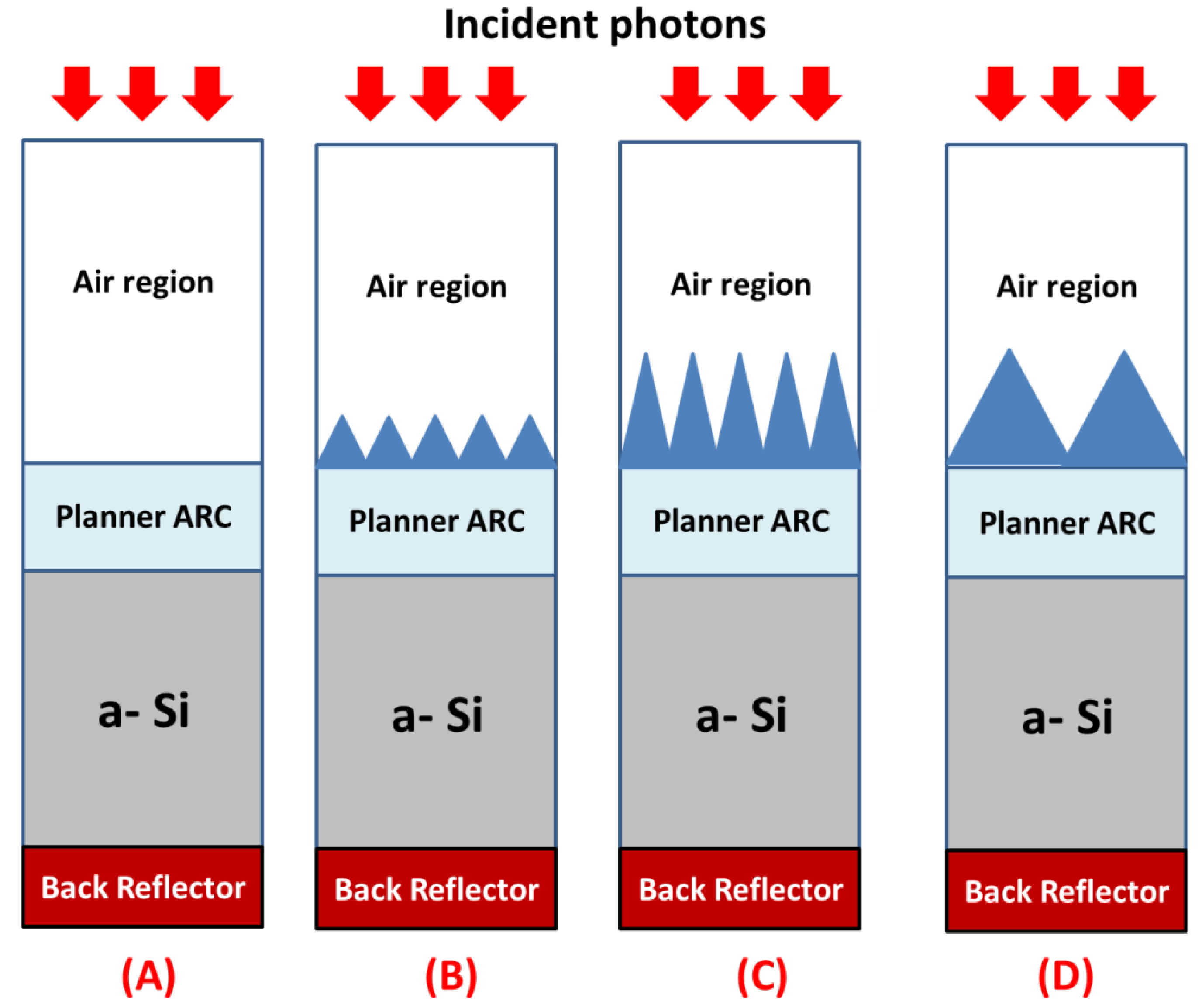
Figure 1. Schematic structure of amorphous silicon solar cell with different dimensions of texturing anti-reflection coating and back reflector with different shapes in (AD).
Photonics 09 00813 g001
Figure 2. Schematic diagram of texturing surface with a path length of incident photons. (A) 3D structure, (B) side view.
Photonics 09 00813 g002
Figure 3. Hydrogenated amorphous silicon solar cell (a-Si: H) absorption spectrum with anti-reflective coating The binary ARC is composed of silicon dioxide deposed on titanium dioxide with thickness 54 nm and 82 nm, respectively. Also, the ternary ARC is composed of silicon nitride with a thickness of 33 nm immersed between silicon dioxide and titanium dioxide with thicknesses 54 nm and 82 nm, respectively.
Photonics 09 00813 g003
Figure 4. Hydrogenated amorphous silicon solar cell (a-Si: H) absorption spectrum with ternary anti-reflective coating with texturing on the top surface with different heights as shown. The ternary ARC is composed of silicon nitride with a thickness of 33 nm immersed between silicon dioxide and titanium dioxide with a thickness of 54 nm and 82 nm, respectively.
Photonics 09 00813 g004
Figure 5. Spectrum of transmission and reflection for ternary anti-reflecting solar cells made on hydrogenated amorphous silicon (a-Si: H) with texturing on the top surface with heights equal to 50 nm. The ternary ARC is composed of silicon nitride with a thickness of 33 nm immersed between silicon dioxide and titanium dioxide with a thickness of 54 nm and 82 nm, respectively.
Photonics 09 00813 g005
Figure 6. Transmission spectrum for one-dimensional photonic crystals composed of silicon dioxide and silicon, with thicknesses of 40 nm and 75 nm, respectively. The number of periods equals 12.
Photonics 09 00813 g006
Figure 7. Hydrogenated amorphous silicon solar cell (a-Si: H) absorption spectrum with ternary anti-reflective coating with texturing on the top surface with a height equal to 50 nm. The ternary ARC is composed of silicon nitride with a thickness of 33 nm immersed between silicon dioxide and titanium dioxide with a thickness of 54 nm and 82 nm, respectively. Also, the back reflector is composed of silicon dioxide and silicon, with thicknesses of 40 nm and 75 nm, respectively. The number of periods equals 12.
Photonics 09 00813 g007
Figure 8. Hydrogenated amorphous silicon solar cell (a-Si: H) absorption spectrum with ternary anti-reflective coating with texturing on the top surface at different incident angles. The ternary ARC is composed of silicon nitride with a thickness of 33 nm immersed between silicon dioxide and titanium dioxide with a thickness of 54 nm and 82 nm, respectively. Also, the back reflector is composed of silicon dioxide and silicon, with thicknesses of 40 nm and 75 nm, respectively. The number of periods equals 12. These calculations are determined at the planner surface, a texturing surface with a height equal to 25 nm, and a texturing surface with height equal to 50 nm, as shown.
Photonics 09 00813 g008
Figure 9. Hydrogenated amorphous silicon solar cell (a-Si: H) absorption spectrum with ternary anti-reflective coating with texturing on the top surface with a height equal to 50 nm at different incident angles. The ternary ARC is composed of silicon nitride with a thickness of 33 nm immersed between silicon dioxide and titanium dioxide with a thickness of 54 nm and 82 nm, respectively. Also, the back reflector is composed of silicon dioxide and silicon, with thicknesses of 40 nm and 75 nm, respectively. The number of periods equals 12. These calculations are determined at the planner surface and texturing surface with a height equal to 25 nm.
Photonics 09 00813 g009
Figure 10. The optical generation of electron–hole pairs for the same structure as in Figure 9.
Photonics 09 00813 g010
Figure 11. Schematic structure of an amorphous silicon solar cell with two electrodes.
Photonics 09 00813 g011
Figure 12. The refractive index and extinction coefficient of indium–tin–oxide (ITO) as a function of the incident wavelengths.
Photonics 09 00813 g012
Figure 13. Hydrogenated amorphous silicon solar cell (a-Si: H) absorption spectrum with ternary anti-reflective coating, as in Figure 9, is represented by the black line. The replacement of the layer of titanium dioxide with indium tin oxide is represented by the red line.
Photonics 09 00813 g013
Table 1. The average reflection of anti-reflection coating designs for noteworthy findings in the literature in comparison to our work.
Anti-Reflection Coating DesignAverage Reflectance (%)
[400–700 nm]
Reference
Polished silicon35.88[18,25]
Standard silicon solar cell16.23[27]
Rectangular PC profile15.9[40]
Triangular PC profile10.6[40,41]
Circular PC profile17.13[40]
1D rectangular PC26/14.08[42]
1D triangular PC7.01/16.62[42]
1D ternary PCs20.4[20]
1D quadrant PCs7[34]
1D texturing PCs5Our work
Publisher’s Note: MDPI stays neutral with regard to jurisdictional claims in published maps and institutional affiliations.