Abstract
The question of how energy resources can be efficiently used is likewise of fundamental and technological interest. In this opinion, we give a brief overview on developments of harvesting solar energy across different length scales and address some strategies to tackle economic and ecological challenges, in particular with a view to sustainability and toward a circular economy. On the mesoscopic scale, the emergence of thermodynamic laws in open quantum systems is of central importance and how they can be employed for efficient quantum thermal machines and batteries. The broad tunability of band gaps in quantum dot systems makes them attractive for hybrid photovoltaic devices. Complementary, machine learning-aided band gap engineering and the high-throughput screening of novel materials assist with improving absorption characteristics. On the device scale, hybrid concepts of optical control via metasurfaces enable a multitude of functionalities such as a directed re-emission of embedded photoluminescent materials or field enhancement effects from nanostructures. Advanced techniques in computational nanophotonics concern a topology optimization of nanostructured layers together with multiobjective optimization toward specific light management tasks. On the industrial level, modern manufacturers explore 3D printing and flexible solar cell platforms obtained from roll-to-roll technologies. The remote control of solar parks through applications via the Internet of Things opens up new strategies to expand to difficult terrain where human interaction is only required to a limited extent.
The second law of thermodynamics states that heat cannot be entirely converted into work entailing, thus, an upper bound on energy conversion. While mesoscopic heat engines [1,2,3] may operate near Carnot efficiency, they are notoriously lacking a high power output. Away from such quasi-reversible conditions, the heat flow [4,5] and therewith the power generation exhibit an upper bound as well, suggesting control knobs for their optimization [6,7]. In the case of solar energy harvesting, the conversion efficiency regarding conventional single-gap solar cells is limited, as established by Shockley and Queisser [8], to roughly 31%. Multiple-gap devices may extract up to 70% from the solar energy under normal sunlight exposure turning it to electrical work [9]. While single-junction devices are known to achieve efficiencies near the Shockley–Queisser limit as in the case of gallium arsenide thin-film solar cells [10,11], Geisz et al. [12] reported recently that multi-junction devices using III–V compound semiconductors can feature efficiencies of about 39% under normal sunlight and about 47% under high optical concentration.
Such advances in solar energy conversion toward its theoretical limits are an important step for photovoltaics (PV) as key technology for renewable energy harvesting. However, the importance of further increasing the operational lifetime [13,14] and conversion efficiency of PV devices under varying climatic and seasonal weather conditions [15,16], reducing their fabrication costs across the whole value chain, and considering aspects of recycling [17,18] in their overall environmental footprint cannot be underestimated. This demands a joint effort of different scientific communities starting from atomic-scale material science up to industrial-scale system optimization [19]. Bridging these scales plays a vital role in the future success of novel photovoltaic technologies and requires novel multiscale modeling and characterization approaches.
The exploration of novel materials on the mesoscopic scale is a promising route to improve material response [20] and discover innovative material concepts such as perovskites solar cells [13,21,22], spectral conversion in rare-earth doped thin films [23], and conductive nitrides [24,25] exploiting plasmonic effects with reduced absorption losses. Such hybrid concepts allow boosting intrinsically low quantum efficiencies in solar energy devices. As an example, energy conversion processes such as up- and down-conversion, as illustrated in Figure 1 for crystalline silicon c-Si, make light far beyond the (double) band gap of the base material accessible to photovoltaic devices through multi-photon processes. Quantum dot photoluminescence as well as emission by rare-earth doped glasses [23] are great candidates to serve as spectral converters in novel layers. It is projected for standard crystalline silicon solar cells that layers with spectral converters or nanoparticles can add another 2 to 3 percentage points to the energy conversion efficiency further enabling thin-film technologies and increasing their competitiveness with conventional as well as other regenerative energy sources [19]. The characterization of material systems and interfaces involving photon, electron, and plasmon dynamics as well as the study of intrinsic transport and absorption rates are of particular interest. High-throughput computational design [26,27], machine learning optimized property prediction [28,29,30], and screening [31] supplements the band gap engineering [32,33].
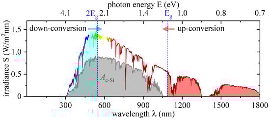
Figure 1.
Solar irradiance S according to the global standard spectrum AM1.5g together with the solar power absorbed by undoped crystalline silicon bulk material. The (indirect) band gap energy of silicon is highlighted together with the double band gap edge. Spectral converters allow re-emitting light toward the photo-active spectral region of a solar cell. The transfer of energy to higher (up-conversion) or lower (down-conversion) energies via multi-photon processes can boost absorption in the solar cells when re-emitting light closer to the Si band gap edge employing quantum dots, rare earths and other materials.
On the device scale, promising photo-active materials are combined with particles, metamaterials and surfaces, adding concepts of optical control to light harvesting in order to exploit scattering, waveguiding and local field enhancement effects [34,35]. Nanoparticle fabrication techniques [19,36] have made tremendous advances in the past decades, in chemical synthesis (etching), lithography, self-assembly through (laser) annealing, and nanoimprint [37]. Typically, self-assembly and chemical synthesis strategies yield random nanoparticle distributions at reduced costs, while lithography techniques allow for high precision in geometrical size, shape, and placement within nanometer resolution. Near-field effects play an important role when exploiting nanostructured surfaces within solar cells. Engineering their interface is necessary in order to generate high local fields at both absorption and re-emission energies. Ultimately, metasurfaces with a multitude of functionalities such as the directed re-emission of embedded photoluminescent materials would be highly beneficial. The integrated electro-optical modeling of solar cells needs to address doped semiconductors and interaction effects between free carriers, such as free carrier absorption [25]. Components in large-scale, electro-optical devices and photonic circuits are subject to interaction phenomena stemming from light–matter coupling at the nanoscale. The study of integrated semi-classical theories addressing electron–electron, electron–photon and electron–phonon interactions is essential for an accurate description of applications with nanoscale features and complex mesoscale dynamics while at the same time maintaining feasible computational times.
Within computational nanophotonics, a multitude of numerical approaches are available each with its very own advantages and disadvantages [38]. Electrodynamics is in itself multiscalar from isolated nanoparticles to large-area, multi-layered devices. One major aim in multiscalar, integrated modeling of electro-optical devices is to maintain the computational advantages and availability of existing analytic and numerical tools. Spectral tuning of the scattering properties of nanostructured surfaces is vital to avoid detrimental effects due to absorption in additional front surface layers. Nanoparticles are efficient subwavelength scatterers improving the light trapping effect and, in particular, metal nanoparticles provide large local fields enhancing charge carrier generation, absorption, and light-induced effects from other nanostructures such as spectral conversion and photoluminescence. Purely optical modeling is challenged by the mutual electronic interaction of doped semiconductor layers, nanoparticles and other photo-active nanostructures, mesoscale electron dynamics and thermal effects that are not captured in classical electrodynamics and standard techniques. A key task is, thus, the integration of electro-optical effects and combined electro-optical coupling. Semi-classical approaches toward mesoscale electron dynamics allow maintaining the advantages of nanophotonic modeling through extended theories [39,40]. Topology optimization [23,41] together with multiobjective optimization [42,43] allow specifying light trapping goals toward broadband absorption for solar technologies. Imprint and template technologies [37] enable the mass fabrication of optimized surface morphology designs at strongly reduced costs once an optimized design has been found. Beyond the performance optimization of photovoltaic devices, the aging due to solar irradiation [44,45] and its mitigation [13,46] is an active field of research having an impact on the materials eventually used.
Large-area additive manufacturing schemes such as 3D printing and roll-to-roll technologies [47] for both solar concentrators [48] and solar cells themselves [49,50,51] have increased the accessibility to renewable solar energy applications at an industrial level. Dealing with solar cell modules in both private households and on corporate property, the storage and power distribution of renewable energies pose major challenges [52,53]. Here, next to highly efficient solar cell modules, novel battery technologies are needed [54,55,56]. Solar parks placed in deserts or facilities on mountain ranges and other locations providing optimum geographical solar irradiation in barely developed areas can strongly benefit from the practical advances being made in connection with remote facility control and the Internet of Things [57]. The dramatic reduction of on-site staff necessary to run, control and maintain such facilities enables building regenerative energy factories in remote areas. Combining local performance monitoring with the Internet of Things allows automated, in situ error correction and feedback control systems that are manageable with little human interaction.
The effective recycling of solar cell modules fully or partially is an ongoing challenge concerning all scales which starts with material choice, continues with module production and extends toward the end of their operational lifetime [17]. Nowadays, the high efficiency and stability of solar cell technologies are tied to the usage of toxic compounds, non-recyclable and scarce materials, and research into the sustainability of these technologies is still modest. Ideally, future research efforts will jointly aim toward a circular PV economy, i.e., manufacturing of solar cells from recycled materials, avoidance of waste during the production process, increasing the possibility to repair or refurbish aging cells, as well as reusing parts in remanufacturing strategies [18]. Some PV technologies allow extending the cell’s lifetime where, e.g., the rehydration of electrolyte-based platforms such as dye-sensitized solar cells [58,59] would enable their continued usage in agriculture or outdoor settings.
We wish to highlight some advances in photovoltaic technologies bringing together different scientific communities as recently published in the special issue Advances in Photovoltaic Technologies from Atomic to Device Scale that we guest edited. Indium phosphide nanodisk array coatings for thin-film silicon based solar cells are proposed by Kjellberg et al. [60] as an antireflective layer with the purpose of improving the solar cell’s absorption efficiency in the visible spectrum. The coatings themselves enable the generation of minority carriers being accessible for charge extraction. Building-integrated photovoltaics considers PV devices as construction and design elements imposing further requirements on their functionality and aesthetics. Against this background, Amores et al. [61] investigate titanium dioxide nanoresonator arrays for solar cell glass covers in order to integrate structured coloring into the devices as well as to reduce the UV transmittance. The latter targets the enhancement of the devices’ lifetime expectancy. Yang et al. [62] present a novel approach to prepare high-quality perovskite photoelectric devices by incorporating cesium lead iodide quantum dots. The authors experimentally prove that the quantum dots can passivate defects in the perovskite’s active layer, improving its morphology and therewith the device’s performance. Furthermore, the environmental stability of the perovskite film is increased. Last but not least, Jian and Cao [63] discuss how to identify parameters of photovoltaic devices from measured current–voltage characteristics by mapping them to an effective model. This allows a comparison of the performances of distinct setups on equal footing under environmental conditions and enables to infer temperature and irradiation effects.
We hope the special issue related to this opinion piece is inspiring and instrumental for further research on photovoltaic devices.
Author Contributions
Writing—original draft preparation, C.D., R.H.; visualization, C.D. All authors have read and agreed to the published version of the manuscript.
Funding
This research received no external funding.
Data Availability Statement
Not applicable.
Conflicts of Interest
The authors declare no conflict of interest.
References
- Jordan, A.N.; Sothmann, B.; Sánchez, R.; Büttiker, M. Powerful and efficient energy harvester with resonant-tunneling quantum dots. Phys. Rev. B 2013, 87, 075312. [Google Scholar] [CrossRef]
- Sánchez, R.; Burset, P.; Yeyati, A.L. Cooling by Cooper pair splitting. Phys. Rev. B 2018, 98, 241414. [Google Scholar] [CrossRef]
- Hussein, R.; Governale, M.; Kohler, S.; Belzig, W.; Giazotto, F.; Braggio, A. Nonlocal thermoelectricity in a Cooper-pair splitter. Phys. Rev. B 2019, 99, 075429. [Google Scholar] [CrossRef]
- Bekenstein, J.D. Energy Cost of Information Transfer. Phys. Rev. Lett. 1981, 46, 623. [Google Scholar] [CrossRef]
- Pendry, J.B. Quantum limits to the flow of information and entropy. J. Phys. A 1983, 16, 2161. [Google Scholar] [CrossRef]
- Whitney, R.S. Most Efficient Quantum Thermoelectric at Finite Power Output. Phys. Rev. Lett. 2014, 112, 130601. [Google Scholar] [CrossRef]
- Whitney, R.S. Finding the quantum thermoelectric with maximal efficiency and minimal entropy production at given power output. Phys. Rev. B 2015, 91, 115425. [Google Scholar] [CrossRef]
- Shockley, W.; Queisser, H.J. Detailed Balance Limit of Efficiency of p-n Junction Solar Cells. J. Appl. Phys. 1961, 32, 510. [Google Scholar] [CrossRef]
- Martí, A.; Araújo, G.L. Limiting efficiencies for photovoltaic energy conversion in multigap systems. Sol. Energy Mater. Sol. Cells 1996, 43, 203. [Google Scholar] [CrossRef]
- Vossier, A.; Gualdi, F.; Dollet, A.; Ares, R.; Aimez, V. Approaching the Shockley-Queisser limit: General assessment of the main limiting mechanisms in photovoltaic cells. J. Appl. Phys. 2015, 117, 015102. [Google Scholar] [CrossRef]
- Green, M.A.; Dunlop, E.D.; Hohl-Ebinger, J.; Yoshita, M.; Kopidakis, N.; Bothe, K.; Hinken, D.; Rauer, M.; Hao, X. Solar cell efficiency tables (Version 60). Prog. Photovolt. Res. Appl. 2022, 30, 687. [Google Scholar] [CrossRef]
- Geisz, J.F.; France, R.M.; Schulte, K.L.; Steiner, M.A.; Norman, A.G.; Guthrey, H.L.; Young, M.R.; Song, T.; Moriarty, T. Six-junction III-V solar cells with 47.1under 143 Suns concentration. Nat. Energy 2020, 5, 326. [Google Scholar] [CrossRef]
- Wang, Q.; Phung, N.; Di Girolamo, D.; Vivo, P.; Abate, A. Enhancement in lifespan of halide perovskite solar cells. Energy Environ. Sci. 2019, 12, 865. [Google Scholar] [CrossRef]
- Godin, R.; Durrant, J.R. Dynamics of photoconversion processes: The energetic cost of lifetime gain in photosynthetic and photovoltaic systems. Chem. Soc. Rev. 2021, 50, 13372. [Google Scholar] [CrossRef] [PubMed]
- Alonso-Abella, M.; Chenlo, F.; Nofuentes, G.; Torres-Ramírez, M. Analysis of spectral effects on the energy yield of different PV (photovoltaic) technologies: The case of four specific sites. Energy 2014, 67, 435. [Google Scholar] [CrossRef]
- Eke, R.; Betts, T.R.; Gottschalg, R. Spectral irradiance effects on the outdoor performance of photovoltaic modules. Renew. Sust. Energ. Rev. 2017, 69, 429. [Google Scholar] [CrossRef]
- Tao, J.; Yu, S. Review on feasible recycling pathways and technologies of solar photovoltaic modules. Sol. Energy Mater. Sol. Cells 2015, 141, 108. [Google Scholar] [CrossRef]
- Schoden, F.; Dotter, M.; Knefelkamp, D.; Blachowicz, T.; Schwenzfeier Hellkamp, E. Review of State of the Art Recycling Methods in the Context of Dye Sensitized Solar Cells. Energies 2021, 14, 3741. [Google Scholar] [CrossRef]
- Abu Hamed, T.; Adamovic, N.; Aeberhard, U.; Alonso-Alvarez, D.; Amin-Akhlaghi, Z.; Auf der Maur, M.; Beattie, N.; Bednar, N.; Berland, K.; Birner, S.; et al. Multiscale in modelling and validation for solar photovoltaics. EPJ Photovolt. 2018, 9, 10. [Google Scholar] [CrossRef]
- Maiti, S.; van der Laan, M.; Poonia, D.; Schall, P.; Kinge, S.; Siebbeles, L.D.A. Emergence of new materials for exploiting highly efficient carrier multiplication in photovoltaics. Chem. Phys. Rev. 2020, 1, 011302. [Google Scholar] [CrossRef]
- Raja, W.; De Bastiani, M.; Allen, T.G.; Aydin, E.; Razzaq, A.; Rehman, A.U.; Ugur, E.; Babayigit, A.; Subbiah, A.S.; Isikgor, F.H.; et al. Photon recycling in perovskite solar cells and its impact on device design. Nanophotonics 2020, 10, 2023. [Google Scholar] [CrossRef]
- Wu, T.; Qin, Z.; Wang, Y.; Wu, Y.; Chen, W.; Zhang, S.; Cai, M.; Dai, S.; Zhang, J.; Liu, J.; et al. The Main Progress of Perovskite Solar Cells in 2020–2021. Nanomicro Lett. 2021, 13, 152. [Google Scholar] [CrossRef] [PubMed]
- Lakhotiya, H.; Nazir, A.; Madsen, S.P.; Christiansen, J.; Eriksen, E.; Vester-Petersen, J.; Johannsen, S.R.; Jeppesen, B.R.; Balling, P.; Larsen, A.N.; et al. Plasmonically enhanced upconversion of 1500 nm light via trivalent Er in a TiO2 matrix. Appl. Phys. Lett. 2016, 109, 263102. [Google Scholar] [CrossRef]
- Zakutayev, A. Design of nitride semiconductors for solar energy conversion. J. Mater. Chem. A 2016, 4, 6742. [Google Scholar] [CrossRef]
- David, C.; Koduvelikulathu, L.J.; Kopecek, R. Comparative Simulations of Conductive Nitrides as Alternative Plasmonic Nanostructures for Solar Cells. Energies 2021, 14, 4236. [Google Scholar] [CrossRef]
- Curtarolo, S.; Hart, G.L.W.; Nardelli, M.B.; Mingo, N.; Sanvito, S.; Levy, O. The high-throughput highway to computational materials design. Nat. Mater. 2013, 12, 191. [Google Scholar] [CrossRef]
- Shen, L.; Zhou, J.; Yang, T.; Yang, M.; Feng, Y.P. High-Throughput Computational Discovery and Intelligent Design of Two-Dimensional Functional Materials for Various Applications. Acc. Mater. Res. 2022, 3, 572–583. [Google Scholar] [CrossRef]
- Pilania, G.; Mannodi-Kanakkithodi, A.; Uberuaga, B.P.; Ramprasad, R.; Gubernatis, J.E.; Lookman, T. Machine learning bandgaps of double perovskites. Sci. Rep. 2016, 6, 19375. [Google Scholar] [CrossRef]
- Zhuo, Y.; Mansouri Tehrani, A.; Brgoch, J. Predicting the Band Gaps of Inorganic Solids by Machine Learning. J. Phys. Chem. Lett. 2018, 9, 1668. [Google Scholar] [CrossRef]
- Hussein, R.; Schmidt, J.; Barros, T.; Marques, M.A.L.; Botti, S. Machine-learning correction to density-functional crystal structure optimization. MRS Bulletin 2022, 47, 765. [Google Scholar] [CrossRef]
- Castelli, I.E.; Olsen, T.; Datta, S.; Landis, D.D.; Dahl, S.; Thygesen, K.S.; Jacobsen, K.W. Computational screening of perovskite metal oxides for optimal solar light capture. Energy Environ. Sci. 2012, 5, 5814. [Google Scholar] [CrossRef]
- Dey, P.; Bible, J.; Datta, S.; Broderick, S.; Jasinski, J.; Sunkara, M.; Menon, M.; Rajan, K. Informatics-aided bandgap engineering for solar materials. Comput. Mater. Sci. 2014, 83, 185. [Google Scholar] [CrossRef]
- De Bastiani, M.; Mirabelli, A.J.; Hou, Y.; Gota, F.; Aydin, E.; Allen, T.G.; Troughton, J.; Subbiah, A.S.; Isikgor, F.H.; Liu, J.; et al. Efficient bifacial monolithic perovskite/silicon tandem solar cells via bandgap engineering. Nat. Energy 2021, 6, 167. [Google Scholar] [CrossRef]
- Polman, A.; Atwater, H.A. Photonic design principles for ultrahigh-efficiency photovoltaics. Nat. Mater. 2012, 11, 174. [Google Scholar] [CrossRef] [PubMed]
- Ai, B.; Fan, Z.; Wong, Z.J. Plasmonic-perovskite solar cells, light emitters, and sensors. Microsyst. Nanoeng. 2022, 8, 5. [Google Scholar] [CrossRef]
- David, C.; Connolly, J.P.; Chaverri Ramos, C.; García de Abajo, F.J.; Sánchez Plaza, G. Theory of random nanoparticle layers in photovoltaic devices applied to self-aggregated metal samples. Sol. Energy Mater. Sol. Cells 2013, 109, 294. [Google Scholar] [CrossRef]
- Spinelli, P.; Ferry, V.E.; van de Groep, J.; van Lare, M.; Verschuuren, M.A.; Schropp, R.E.I.; Atwater, H.A.; Polman, A. Plasmonic light trapping in thin-film Si solar cells. J. Opt. 2012, 14, 024002. [Google Scholar] [CrossRef]
- Hohenester, U. Nano and Quantum Optics; Springer: Cham, Switzerland, 2020. [Google Scholar] [CrossRef]
- David, C.; García de Abajo, F.J. Surface Plasmon Dependence on the Electron Density Profile at Metal Surfaces. ACS Nano 2014, 8, 9558. [Google Scholar] [CrossRef]
- David, C.; Christensen, J.; Mortensen, N.A. Spatial dispersion in two-dimensional plasmonic crystals: Large blueshifts promoted by diffraction anomalies. Phys. Rev. B 2016, 94, 165410. [Google Scholar] [CrossRef]
- Sigmund, O. EML webinar overview: Topology Optimization—Status and Perspectives. Extreme Mech. Lett. 2020, 39, 100855. [Google Scholar] [CrossRef]
- Sun, R.; Guo, J.; Wu, Q.; Zhang, Z.; Yang, W.; Guo, J.; Shi, M.; Zhang, Y.; Kahmann, S.; Ye, L.; et al. A multi-objective optimization-based layer-by-layer blade-coating approach for organic solar cells: Rational control of vertical stratification for high performance. Energy Environ. Sci. 2019, 12, 3118. [Google Scholar] [CrossRef]
- Zhang, W.W.; Qi, H.; Ji, Y.K.; He, M.J.; Ren, Y.T.; Li, Y. Boosting photoelectric performance of thin film GaAs solar cell based on multi-objective optimization for solar energy utilization. Sol. Energy 2021, 230, 1122. [Google Scholar] [CrossRef]
- Mazouz, H.; Belghachi, A.; Logerais, P.O.; Delaleux, F.; Riou, O. Numerical Simulation of GaAs Solar Cell Aging Under Electron and Proton Irradiation. IEEE J. Photovolt. 2019, 9, 1774. [Google Scholar] [CrossRef]
- Raya-Armenta, J.M.; Bazmohammadi, N.; Vasquez, J.C.; Guerrero, J.M. A short review of radiation-induced degradation of III-V photovoltaic cells for space applications. Sol. Energy Mater. Sol. Cells 2021, 233, 111379. [Google Scholar] [CrossRef]
- Roesch, R.; Eberhardt, K.R.; Engmann, S.; Gobsch, G.; Hoppe, H. Polymer solar cells with enhanced lifetime by improved electrode stability and sealing. Sol. Energy Mater. Sol. Cells 2013, 117, 59. [Google Scholar] [CrossRef]
- Nadagouda, M.N.; Ginn, M.; Rastogi, V. A review of 3D printing techniques for environmental applications. Curr. Opin. Chem. Eng. 2020, 28, 173. [Google Scholar] [CrossRef]
- van Dijk, L.; Marcus, E.A.P.; Oostra, A.J.; Schropp, R.E.I.; Di Vece, M. 3D-printed concentrator arrays for external light trapping on thin film solar cells. Sol. Energy Mater. Sol. Cells 2015, 139, 19. [Google Scholar] [CrossRef]
- Dou, B.; Whitaker, J.B.; Bruening, K.; Moore, D.T.; Wheeler, L.M.; Ryter, J.; Breslin, N.J.; Berry, J.J.; Garner, S.M.; Barnes, F.S.; et al. Roll-to-Roll Printing of Perovskite Solar Cells. ACS Energy Lett. 2018, 3, 2558. [Google Scholar] [CrossRef]
- Knott, A.; Makarovskiy, O.; O’Shea, J.; Wu, Y.; Tuck, C. Scanning photocurrent microscopy of 3D printed light trapping structures in dye-sensitized solar cells. Sol. Energy Mater. Sol. Cells 2018, 180, 103. [Google Scholar] [CrossRef]
- Benitez-Rodriguez, J.F.; Chen, D.; Gao, M.; Caruso, R.A. Roll-to-Roll Processes for the Fabrication of Perovskite Solar Cells under Ambient Conditions. Sol. RRL 2021, 5, 2100341. [Google Scholar] [CrossRef]
- Mishra, S.; Das, D.; Paul, S. A comprehensive review on power distribution network reconfiguration. Energy Syst. 2017, 8, 227. [Google Scholar] [CrossRef]
- Yang, Y.; Bremner, S.; Menictas, C.; Kay, M. Battery energy storage system size determination in renewable energy systems: A review. Renew. Sustain. Energy Rev. 2018, 91, 109. [Google Scholar] [CrossRef]
- Andolina, G.M.; Keck, M.; Mari, A.; Giovannetti, V.; Polini, M. Quantum versus classical many-body batteries. Phys. Rev. B 2019, 99, 205437. [Google Scholar] [CrossRef]
- Pirmoradian, F.; Mølmer, K. Aging of a quantum battery. Phys. Rev. A 2019, 100, 043833. [Google Scholar] [CrossRef]
- Mooraj, S.; Qi, Z.; Zhu, C.; Ren, J.; Peng, S.; Liu, L.; Zhang, S.; Feng, S.; Kong, F.; Liu, Y.; et al. 3D printing of metal-based materials for renewable energy applications. Nano Res. 2021, 14, 2105. [Google Scholar] [CrossRef]
- Emamian, M.; Eskandari, A.; Aghaei, M.; Nedaei, A.; Sizkouhi, A.M.; Milimonfared, J. Cloud Computing and IoT Based Intelligent Monitoring System for Photovoltaic Plants Using Machine Learning Techniques. Energies 2022, 15, 3014. [Google Scholar] [CrossRef]
- Hagfeldt, A.; Grätzel, M. Molecular Photovoltaics. Acc. Chem. Res. 2000, 33, 269. [Google Scholar] [CrossRef]
- Sharma, K.; Sharma, V.; Sharma, S.S. Dye-Sensitized Solar Cells: Fundamentals and Current Status. Nanoscale Res. Lett. 2018, 13, 381. [Google Scholar] [CrossRef]
- Kjellberg, M.; Ravishankar, A.P.; Anand, S. Enhanced Absorption in InP Nanodisk Arrays on Ultra-Thin-Film Silicon for Solar Cell Applications. Photonics 2022, 9, 157. [Google Scholar] [CrossRef]
- Amores, A.P.; Ravishankar, A.P.; Anand, S. Design and Modelling of Metal-Oxide Nanodisk Arrays for Structural Colors and UV-Blocking Functions in Solar Cell Glass Covers. Photonics 2022, 9, 273. [Google Scholar] [CrossRef]
- Yang, G.; Zhou, D.; Li, J.; Yu, J. Passivation Effect of CsPbI3 Quantum Dots on the Performance and Stability of Perovskite Solar Cells. Photonics 2022, 9, 3. [Google Scholar] [CrossRef]
- Jian, X.; Cao, Y. A Chaotic Second Order Oscillation JAYA Algorithm for Parameter Extraction of Photovoltaic Models. Photonics 2022, 9, 131. [Google Scholar] [CrossRef]

Publisher’s Note: MDPI stays neutral with regard to jurisdictional claims in published maps and institutional affiliations. |
© 2022 by the authors. Licensee MDPI, Basel, Switzerland. This article is an open access article distributed under the terms and conditions of the Creative Commons Attribution (CC BY) license (https://creativecommons.org/licenses/by/4.0/).