Communication

Compact Wavelength Selective Crossbar Switch with Cascaded First Order Micro-Ring Resonators

Electrical and Computer Engineering Department, University of California, Santa Barbara, CA 93106, USA
*
Author to whom correspondence should be addressed.
Photonics 2022, 9(2), 60; https://doi.org/10.3390/photonics9020060
Submission received: 27 December 2021 / Revised: 14 January 2022 / Accepted: 17 January 2022 / Published: 24 January 2022
(This article belongs to the Special Issue Advances of Silicon Photonics)

Abstract

:
We demonstrate a compact 4 × 4 wavelength selective switch with 50% fewer electrical signal pads as compared with our previous generation. We report loss and crosstalk for different paths of the switch. We measure median loss of 5.32 dB and worst case crosstalk of −35 dB. The microring resonators tune by more than one free spectral range, which is an improvement over our previous generation of switches. This switch can support 8 channels at 400 GHz spacing. We conclude that it is possible to drive both microring resonators with the same voltage and separate control is not required if the fabrication variation reduces in the future.

1. Introduction

Optical switches in datacenters reduce fiber handling and enable more scalable data centers [1]. A wavelength selective switch (WSS) can switch multiple wavelengths from an input port to output port [2]. WSS on silicon are reported in [3,4,5,6,7,8,9,10,11,12]. Applications of these switches in HyperX datacenter topology is reported in [1]. We proposed a multi-wavelength selective crossbar switch (MSCS) in [13].
In this paper, we present a 4 × 4 switch with L = 2 (2 cascaded first order Microring resonator (MRR) at every crosspoint) switch that can tune over one full FSR with a more compact footprint. We also show full free spectral tuning of the MRR. MRR spectra are very sensitive to gap between waveguides. For the case of higher order ring resonators specific relationship between multiple coupling coefficients must be met for a flattop spectra. An easier approach to achieve a given 3 dB bandwidth and at the same time a higher out of band rejection is to cascade the drop transmission spectra of multiple first-order ring resonators. This results in a higher power penalty as compared to second order ring resonator, but the ease of design makes this one of the choices for the filter in the 2 λ switch.
4 × 4 switch with L = 2 with second-order cascaded first-order rings has to 64 signal pads and the area of the switch scales as 2 L N 2 . The area of this switch can be reduced by half if both the ring resonator heater are connected together. This places stringent constraints on acceptable resonant wavelength variation of the fabrication process. We measure a switch fabricated in a 220 nm Si Photonics foundry and report the standard deviation of loss, continuous wave (CW) crosstalk, resonant wavelength at zero bias, and full width at half maximum (FWHM).
Improvement in fabrication process will enable better scaling of future switches. We conclude that, one can build switches by connecting the signals of the two ring resonators to the same pad if the MRR uniformity improves. We compare two different chips and measure the dissimilarity between two rings by recording the voltage applied at the two rings.

2. Architecture

In the next few paragraphs, describe the architecture of the switch. Figure 1a shows a N × N switch with M wavelengths at each input port. We need only L = 2, i.e., two MRR per crosspoint for near optimal latency [13]. Figure 1b Tx corresponds to transmitter and Rx corresponds to receiver. Figure 1c shows switch unit cell. Figure 1d shows layout of a 4 × 4 L = 2 switch. Figure 1e shows micro graph of 4 × 4 L = 2 switch. The MRR are tuned using thermal tuning. We built the switch using MRR from AIM photonics process design kit (PDK).
Time is divided into timeslots and at the start of every timeslot a centralized arbiter performs scheduling of traffic and wavelength assignment. More information about assignment and arbitration can be found in [4]. At the start of every timeslot the arbitration algorithm generates a traffic matrix. Each entry in the traffic matrix corresponds to number of wavelength channels required between input and output ports.

3. Results

In the next few paragraphs, we report experimental results of the switch. Figure 2a shows the measured transfer spectra comparison of one and two cascaded first-order ring resonators. The out-of-band rejection 400 GHz away from resonance wavelength of ring resonator increases from −21 dB to −40 dB as we change the ring filter from one to two cascaded filters. The 3 dB bandwidth of the cascaded ring resonator changes from 64 GHz to 38 GHz. This is the expected 3 dB bandwidth of the cascaded filters. The curve in red shows the measured cascaded filter response from one of the unit cells in the switch. The filter 3 dB bandwidth is 40 GHz which is larger than the expected 3 dB bandwidth of 38 GHz because the heaters of the two ring resonators are tied together. Thus, individual control of resonators is not possible and any misalignment between the resonators changes the filter shape. The extinction on the through port is −17 dB.
Figure 2b shows the tuning curve of the cascaded first order ring filter. In this measurement, an increasing voltage is applied to one cascaded ring from a unit cell of the 4 × 4 switch. The ring tunes by 27.06 nm/25.6 nm with a tuning efficiency of 0.37 nm/mW (for both rings). This ring tunes by more than Free Spectral Range (FSR) and thus can be used for selecting all WDM channels present in the system. The MRR can support 8 wavelength division multiplexed (WDM) channels at 400 GHz spacing. The peak of the drop spectrum decreases with wavelength as the polarization controller is not tuned for every voltage applied to the ring signal pad. We automated the measurements with functions from Lumos, an instrument control library in python [14]. We use MRR from founndry process design kit (PDK) in this paper. We advise the reader to use MRR reported in [15] for a lower off resonance loss.
The low loss and full FSR tuning make this MRR an ideal candidate for opto-electronic switches. Tuning curve and Heater I-V and R-V are reported in Figure 2c,d. The tuning curve demonstrates full FSR tuning. The resonance wavelength is 1536.9 nm and the histogram of resonant wavelengths measured on different filters on the die is given in Figure 3a. Heater I-V in Figure 2d shows that the current changes from 6 mA to 20 mA as the voltage changes from 0 to 3.7 mA. The resistance changes from 80 Ω to 180 Ω . This I-V curve is explained by the self heating effect [16].
We compare our results with other notable wavelength selective silicon photonic switches in Table 1. In this work, best and worst case path loss was worse than our best switch [7]. This was due to misalignment of the drop port spectrum peak of the cascaded ring resonators. Out of band rejection is better than all the other wavelength selective switches reported in the table. This is due to cascading of two first order switches as shown in Figure 1c and Figure 2a.
There are in total 32 signal pads and 16 ground pads with a total footprint of 1.6 × 1.55 mm 2 . The signals were routed with a 1 μ m/mA rule to avoid burnout due to electro migration. The layout was done with Cadence Virtuoso and waveguide crossings were designed using Phoenix Optodesigner. Traces of 70 μ m and 20 μ m are used to connect to the ground pads. Due to the low measured resistance of the ring resonators, traces with twice the width or connecting all grounds to a ground plane on a different electrical routing layer might be a better choice for future switches. Pad sizes are 60 μ m × 60 μ m with a pitch of 160 μ m. A pitch of <135 μ m is unsuitable for flip-chip bonding to organic carriers and we choose this pitch even though we did not flip chip this chip in this work. All pads were filled with square vias, as larger number of vias connecting different pad layers prevent pad peel off problem.
The waveguide dimension used in routing is 220 nm × 400 nm and we use 5 μ m radius bends for routing all waveguides. Foundry-specified waveguide loss is 2 dB/cm and edge coupler loss is 2.7 dB/facet. A 100 μ m trench is provided at the chip edge for ease of optical coupling. Waveguide crossings are designed with particle swarm optimization and have a reported average loss of 0.028 dB and worst-case crosstalk of 37 dB [18]. The designed footprint of the crossing is 17 μ m × 17 μ m due to 4 μ m linear tapers used to taper the waveguide from 400 nm to 500 nm. Spirals with simultaneous tapered width from 400 nm to 150 nm and radius from 5 μ m to 0.2 μ m are used for waveguide termination. These spirals have a 20-dB reflection simulated with Lumerical 3D Finite Difference Time Domain package at 1550 nm.
Figure 4a shows transmission (dB) vs. paths in the 4 × 4 switch. Blue dots correspond to measured data points at different wavelengths and red corresponds to median of the points for each path. Figure 4b shows a median loss of 5.32 dB. Median is used instead of mean due to skewed distribution of the data. The outliers in Figure 4a,b correspond to cascaded filters with a large difference of resonant wavelengths. Continuous wave (CW) off loss is measured at 1546.8 nm. MRRs with lower off resonance pass through loss will reduce the optical path loss of the switch. Figure 4c,d, shows the crosstalk measurement. We set a MRR on a chosen path ring to 1546.8 nm and we measure the crosstalk power at other ports.
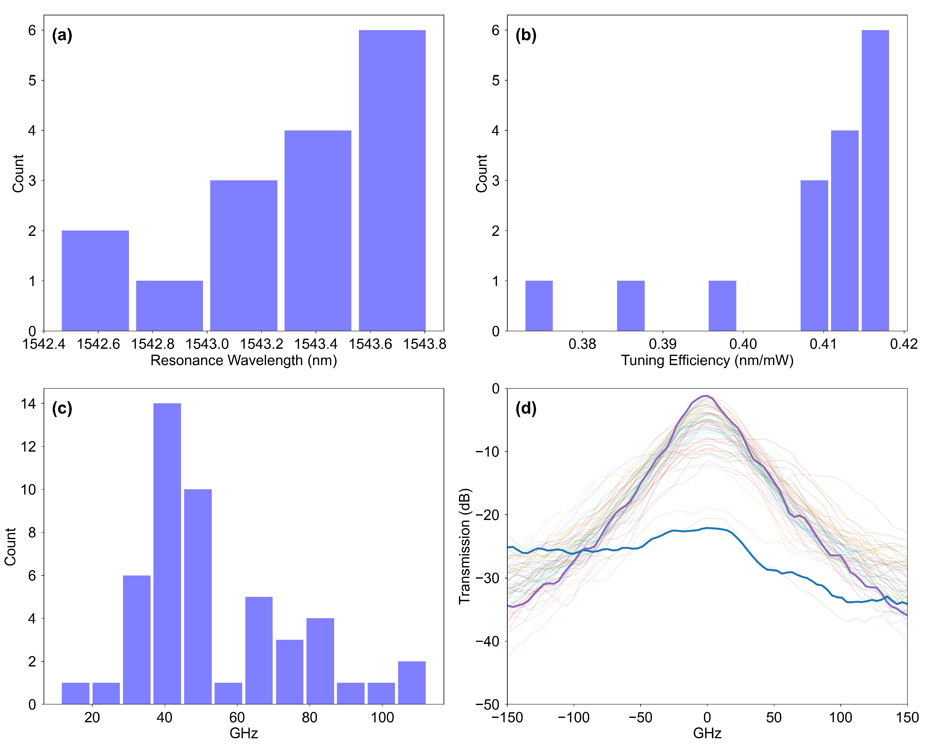
Figure 3a shows the histogram of resonant wavelengths with mean of 1543.4 nm and standard deviation of 0.4 nm. This is similar to the measured standard deviation of 0.3 nm for second order resonators from [4]. These measurements we made on MRRs from a 4 × 4 switch. Figure 3b shows the histogram of tuning efficiency 0.4 nm/mW and standard deviation of 0.012 nm/mW. Figure 3c shows bandwidth histogram with median bandwidth of 48.7 GHz. Figure 3d shows all measured transfer spectra. One can see the outlier spectra where two cascaded second order MRRs have dissimilar resonant wavelengths.

4. Discussion

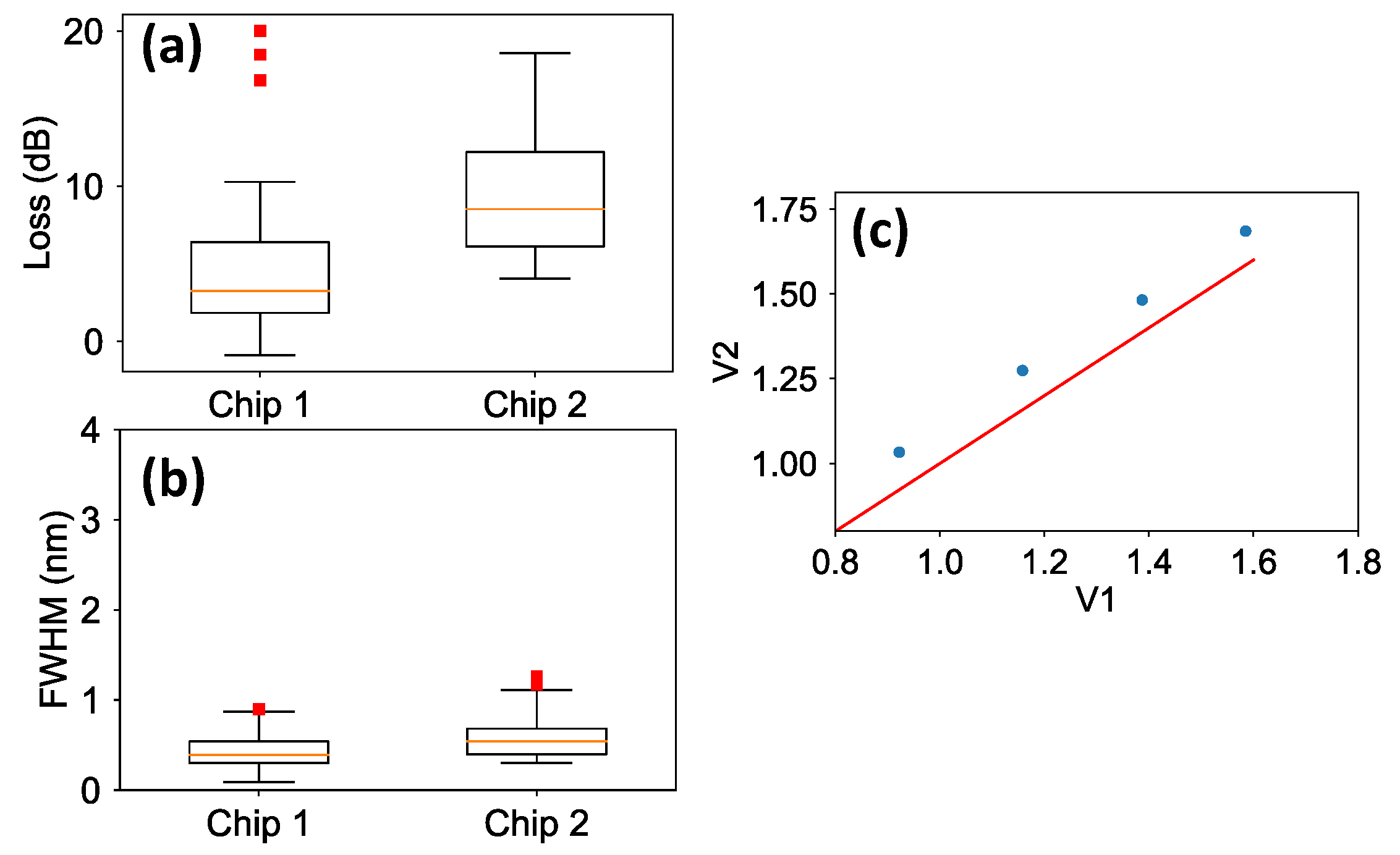
Figure 5a shows a comparison of path loss on two different chips chip1 and chip2. We measured a 4 × 4 switch with cascaded MRRs with signal connected to the same electrical pad. Both chip1 and chip2 have switches where both rings in the cascaded MRR are driven by same signal pad.The orange lines correspond to the median loss. One can see that the median loss of chip 1 is 3.23 dB which is smaller than 8.53 dB of chip 2. The distribution of path losses of chip 2 is skewed towards lower values. The red squares are outliers. Figure 5b shows the FWHM of chip1 and chip 2. The median FWHM of chip 1 is 0.435 nm which is smaller than 0.54 nm of chip 2. The IQR of chip 1 is 0.56 nm which is much greater than 0.29 nm of chip 2. This shows that there is a smaller variation in FWHM values. Figure 5c shows V1 and V2 applied to two rings on a test structure cascaded in the same arrangement as the rings on the switch. These voltages are optimized for maximum peak transmission of a given channel wavelength. Red line shows V 1 = V 2 . The dissimilarity of the drive voltages could be due to two factors, variation in heater resistances or variation in the fabrication process (thickness of the chip). As the rings are placed right next to each other it is unlikely that thickness can be a factor. Different doping of resistors or other fabrication variation that can change dimensions of the resistors can change the effective index of the ring resonator. This could be the reason for different resonant wavelength and heater resistances.
We run a simulation to calculate the maximum allowed difference of resonant frequencies of the two first order ring resonators in the cascaded first order rings. Fabrication process should be changed to keep the difference between resonant wavelengths of the first order MRRs in the cascaded MRRs within this value. When the two MRRs have a different resonant frequency the peak power at the channel of interest drops. Figure 3d shows different peak powers for multiple cascaded MRRs due to the difference in resonant frequencies of the two first order MRRs. We set the maximum value of this power drop to 1 dB below the maximum of the drop spectrum of a first order MRR. This value is much smaller than the receiver margin which is the difference between receiver sensitivity and the maximum path loss of the switch. Maximum path loss of the switch is a very small value in the absence of fabrication variation. There can be more components in the path of light between the output facet of the switch and the receiver. This is why we set the value to 1 dB. The maximum difference in resonant frequency of the first order MRRs is 9.76 GHz.

5. Conclusions

We report a compact switch with same drive for two cascaded MRRs. We report a median path loss of 5.32 dB. The MRRs in the switch can tune across an entire FSR which is an improvement over our previous switches. We conclude that with smaller fabrication variation of the technology, we can drive cascaded MRRs with the same drive voltage in the future.

Author Contributions

Conceptualization, A.S.P.K.; methodology, A.S.P.K.; software, A.S.P.K., R.Z.; project administration, R.H., R.C.A., A.A.M.S., J.E.B. All authors have read and agreed to the published version of the manuscript.

Funding

This work was supported by the U.S. Department of Defense under the AIM Photonics Manufacturing Innovation Institute, Air Force Contract FA8650-15-2-5220.

Conflicts of Interest

The authors declare no conflict of interest.

References

  1. Saleh, A.A.M.; Khope, A.S.P.; Bowers, J.E.; Alferness, R.C. Elastic WDM switching for scalable data center and HPC interconnect networks. In Proceedings of the OptoElectronics and Communications Conference (OECC), Niigata, Japan, 3–7 July 2016; pp. 1–3. [Google Scholar]
  2. Khope, A.S.P.; Samanta, A.; Xiao, X.; Yoo, B.; Bowers, J.E. Review Of Integrated Photonic Elastic WDM Switches For Data Centers. arXiv 2021, arXiv:2105.14934. [Google Scholar]
  3. Xiao, X.; Proietti, R.; Werner, S.; Fotouhi, P.; Yoo, S.B. Flex-LIONS: A scalable silicon photonic bandwidth-reconfigurable optical switch fabric. In Proceedings of the 2019 24th OptoElectronics and Communications Conference (OECC) and 2019 International Conference on Photonics in Switching and Computing (PSC), Fukuoka, Japan, 7–11 July 2019; pp. 1–3. [Google Scholar]
  4. Khope, A.S.; Saeidi, M.; Yu, R.; Wu, X.; Netherton, A.M.; Liu, Y.; Zhang, Z.; Xia, Y.; Fleeman, G.; Spott, A.; et al. Multi-wavelength selective crossbar switch. Opt. Express 2019, 27, 5203–5216. [Google Scholar] [CrossRef] [PubMed]
  5. Seok, T.J.; Luo, J.; Huang, Z.; Kwon, K.; Henriksson, J.; Jacobs, J.; Ochikubo, L.; Muller, R.S.; Wu, M.C. Silicon photonic wavelength cross-connect with integrated MEMS switching. APL Photonics 2019, 4, 100803. [Google Scholar] [CrossRef]
  6. Xiao, X.; Proietti, R.; Liu, G.; Lu, H.; Zhang, Y.; Yoo, S.B. Multi-FSR Silicon Photonic Flex-LIONS Module for Bandwidth-Reconfigurable All-to-All Optical Interconnects. J. Light. Technol. 2020, 38, 3200–3208. [Google Scholar] [CrossRef]
  7. Khope, A.S.P.; Liu, S.; Zhang, Z.; Netherton, A.M.; Hwang, R.L.; Wissing, A.; Perez, J.; Tang, F.; Schow, C.; Helkey, R.; et al. 2 λ switch. Opt. Lett. 2020, 45, 5340–5343. [Google Scholar] [CrossRef] [PubMed]
  8. Khope, A.S.; Helkey, R.; Liu, S.; Khope, S.; Alferness, R.C.; Saleh, A.A.; Bowers, J.E. Scalable multicast hybrid broadband-crossbar wavelength selective switch: Proposal and analysis. Opt. Lett. 2021, 46, 448–451. [Google Scholar] [CrossRef] [PubMed]
  9. Khope, A.S.; Hirokawa, T.; Netherton, A.M.; Saeidi, M.; Xia, Y.; Volet, N.; Schow, C.; Helkey, R.; Theogarajan, L.; Saleh, A.A.; et al. On-chip wavelength locking for photonic switches. Opt. Lett. 2017, 42, 4934–4937. [Google Scholar] [CrossRef] [Green Version]
  10. Huang, Y.; Cheng, Q.; Rizzo, A.; Bergman, K. High-Performance Microring-Assisted Space-and-Wavelength Selective Switch. In Proceedings of the Optical Fiber Communication Conference (OFC), San Diego, CA, USA, 8–12 March 2020; pp. 1–3. [Google Scholar]
  11. Khope, A.S.P.; Helkey, R.; Liu, S.; Saleh, A.A.M.; Alferness, R.C.; Bowers, J.E. A Scalable Multicast Hybrid Broadband Crossbar Wavelength Selective Switch For Datacenters. In Proceedings of the 2021 IEEE 11th Annual Computing and Communication Workshop and Conference (CCWC), NV, USA, 27–30 January 2021; pp. 1585–1587. [Google Scholar] [CrossRef]
  12. Khope, A.S.; Liu, S.; Netherton, A.; Zhang, Z.; Khope, S.; Helkey, R.; Saleh, A.A.; Alferness, R.C.; Bowers, J.E. Experiments on Multiwavelength Selective Crossbar Switches. In Proceedings of the 2020 International Conference on Information Science and Communications Technologies (ICISCT), Tashkent, Uzbekistan, 4–6 November 2020; pp. 1–5. [Google Scholar] [CrossRef]
  13. Khope, A.S.P.; Saleh, A.A.M.; Bowers, J.E.; Alferness, R.C. Elastic WDM crossbar switch for data centers. In Proceedings of the IEEE Optical Interconnects (OI) Conference, San Diego, CA, USA, 9–11 May 2016; pp. 48–49. [Google Scholar]
  14. Khope, A.S.P. Lumos: A Python Instrument Control Library for Photonics. Preprints 2021, 2021060015. [Google Scholar] [CrossRef]
  15. Khope, A.S.P. Ultralow Loss Adiabatic Microring Resonator With Thermal Tuning. Preprints 2021, 2021060186. [Google Scholar] [CrossRef]
  16. Bahadori, M.; Gazman, A.; Janosik, N.; Rumley, S.; Zhu, Z.; Polster, R.; Cheng, Q.; Bergman, K. Thermal Rectification of Integrated Microheaters for Microring Resonators in Silicon Photonics Platform. J. Light. Technol. 2018, 36, 773–788. [Google Scholar] [CrossRef]
  17. Ikeda, K.; Suzuki, K.; Konoike, R.; Kawashima, H. Silicon Photonics Wavelength Selective Switch with Unlimited Free Spectral Range. J. Light. Technol. 2020, 38, 3268–3272. [Google Scholar] [CrossRef]
  18. Ma, Y.; Zhang, Y.; Yang, S.; Novack, A.; Ding, R.; Lim, A.E.J.; Lo, G.Q.; Baehr-Jones, T.; Hochberg, M. Ultralow loss single layer submicron silicon waveguide crossing for SOI optical interconnect. Opt. Express 2013, 21, 29374–29382. [Google Scholar] [CrossRef] [PubMed]
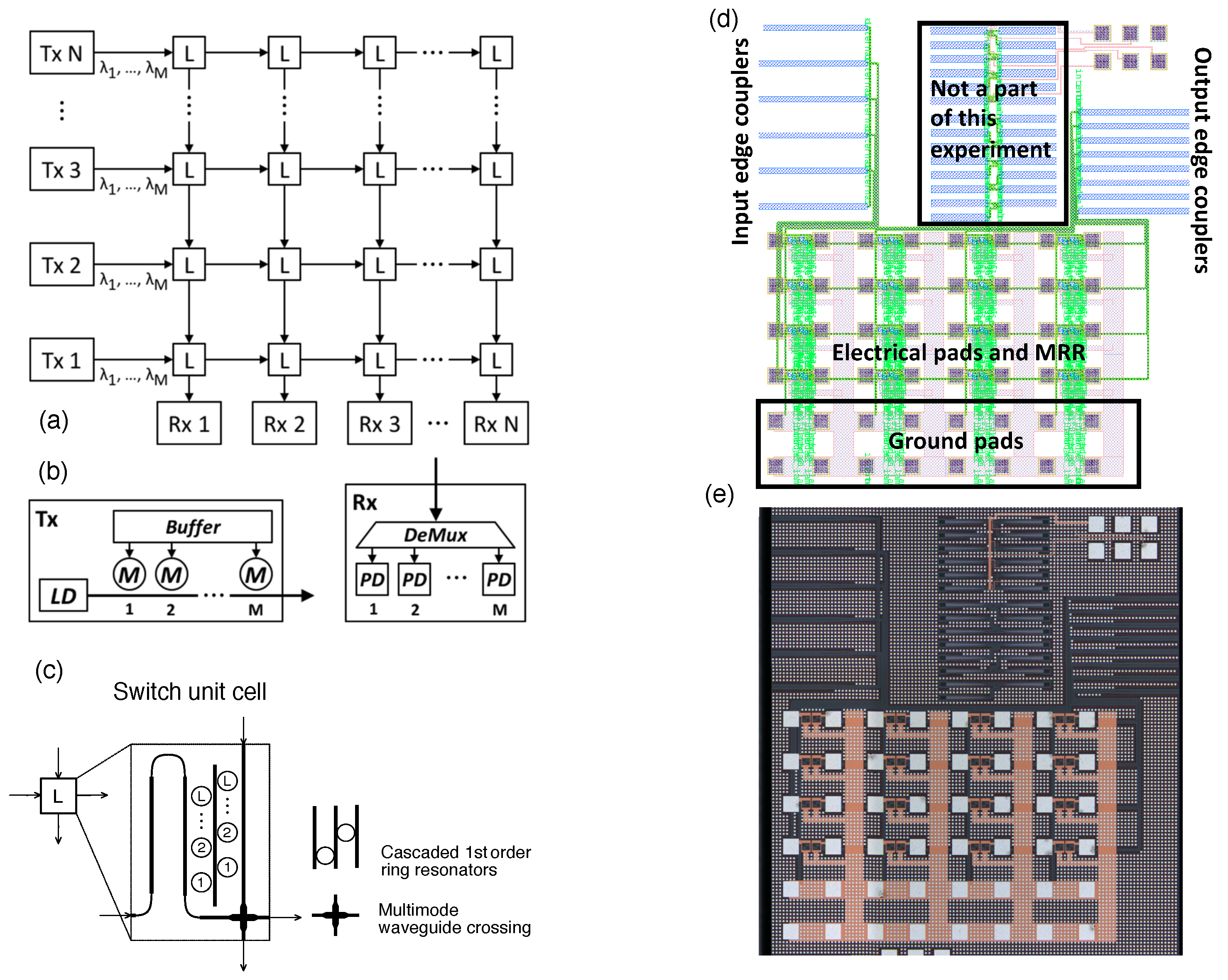
Figure 1. (a) N × N switch with L blocks. M wavelengths are input into the switch. (b) Tx: Transmitter, M microring modulators each driving one wavelength, Shared buffer so that data to any port can be modulated on any modulator [13]. (c) Contents on the L block. L cascaded first order microring resonators and waveguide crossing is used. (d) Layout of 4 × 4 switch and (e) Die shot of 4 × 4 switch.
Photonics 09 00060 g001
Figure 2. Measurements on cascaded first order ring resonator (a) Drop and through transfer spectra of a single first order ring resonator, Expected transfer spectra of cascaded order ring and the best measured cascaded ring, (b) Tuning curve of cascaded ring in a unit cell arrangement where bias is applied to only one ring, (c) Full FSR tuning is demonstrated. The ring tunes by 27.06 nm (>FSR = 25.6 nm) with power efficiency of 0.37 nm/mW for two rings. (d) I-V and R-V curves for the cascaded ring resonators. Nonlinear dependence of R vs. V is measured.
Photonics 09 00060 g002
Figure 3. (a) Histogram of resonant wavelength, mean = 1543.4 and standard deviation = 0.39 nm. (b) Tuning efficiency mean = 0.41 nm/mW and standard deviation = 0.012 nm/mW. (c) Bandwidth histogram with median = 48.7 GHz. (d) Transfer spectra of all ring resonator filters.
Photonics 09 00060 g003
Figure 4. (a) Transmission (dB) vs. paths in the switch. Path 14 corresponds to input 1 and output 4. Each data point (blue) corresponds to measurement at a different wavelength. Red line corresponds to line connecting medians. (b) Histogram of Loss for different paths with a median of 5.32 dB. (c) CW crosstalk is measured at 1546.8 nm. This is the signal channel. (d) Worst case crosstalk is −35 dB.
Photonics 09 00060 g004
Figure 5. (a) Path loss comparison for chip 1 and chip 2. Red squares correspond to outliers and orange lines correspond to the median. (b) Full Width Half Maximum (FWHM) of different switches measured on chip 1 and chip 2. (c) A plot of voltage on each ring for maximum transmission. Red line corresponds to a 45-degree line where V1 = V2. V1 and V2 corresponds to voltages on the two MRR in a cascaded first order MRR.
Photonics 09 00060 g005
Table 1. Comparison with other notable silicon photonic multi-wavelength switches. * Inband/outband extinction. ** Worst case power penalty. *** Out of band rejection at 200 and 400 GHz. **** Out of band rejection at 400 GHz.
ReferencesPort CountPath LossCrosstalk
NIAIST [17]
2020
2 × 20.5 dB15/20 dB *
UCD [6]
2020
8 × 8<8.4 dB5.3 dB **
UCB [5]
2018
8 × 88.8–16.4 dB30 dB
UCSB [9]
2019
8 × 85–45 dB35/40 dB ***
UCSB [4]
2019
8 × 46–14 dB20/32 dB ***
UCSB [7]
2020
4 × 40.8–5 dB22/32 dB ***
UCSB
This work
4 × 40.9–20 dB40 dB ****
Publisher’s Note: MDPI stays neutral with regard to jurisdictional claims in published maps and institutional affiliations.