Abstract
The convolution neural network (CNN) is a classical neural network with advantages in image processing. The use of multiport optical interferometric linear structures in neural networks has recently attracted a great deal of attention. Here, we use three 3 × 3 reconfigurable optical processors, based on Mach-Zehnder interferometers (MZIs), to implement a two-layer CNN. To circumvent the random phase errors originating from the fabrication process, MZIs are calibrated before the classification experiment. The MNIST datasets and Fashion-MNIST datasets are used to verify the classification accuracy. The optical processor achieves 86.9% accuracy on the MNIST datasets and 79.3% accuracy on the Fashion-MNIST datasets. Experiments show that we can improve the classification accuracy by reducing phase errors of MZIs and photodetector (PD) noises. In the future, our work provides a way to embed the optical processor in CNN to compute matrix multiplication.
1. Introduction
The computing power of state-of-the-art Artificial Intelligence (AI) equipment increases gradually (doubling every 3.5 months on average). The CNN is used broadly in the decision-making of image classification, speech recognition, and self-driving cars. However, the computational complexity of the CNN is high. The throughput and energy efficiency ratio may soon become a new bottleneck to the electrical device. Matrix multiplication is an essential and computationally intensive step in CNN. Due to the inherent parallelism of optics, the silicon photonic device is a promising optimization platform for linear multiplication and addition calculations (MAC) to reduce computation time from O(N2) to O(1) [1,2].
Implementing any linear transformation matrix through an on-chip reconfigurable multiport interferometer has been researched plentifully in neural networks. Optical neural networks have proven to be promising in computational speed and power efficiency, allowing for increasingly large neural networks. In 2017, Shen et al. proposed an integrated and programmable MZI-based nanophotonic circuit to realize MAC of electrical fully connected neural networks, and its accuracy is 76.7% [3]. In 2018, Bagherian et al. proposed the concept of an all-optical CNN based on an MZI-based nanophotonic circuit, which reduces a fraction of energy compared to state-of-the-art electronic devices [4]. In 2019, Shokraneh et al. implemented a 4 × 4 MZI-based optical processor used in a single-layer neural network [5]. The experimental results show that the optical processor achieves 72% classification accuracy. In 2020, Nahmias et al. investigated the limits of analog electronic crossbar arrays and on-chip photonic linear computing systems, providing a concrete comparison between deep learning and photonic hardware [6]. This paper showed that photonic hardware improves over digital electronics in energy (>102), speed (>103), and compute density (>102). In 2021, Marinis et al. characterized and compared two thermally tuned photonic integrated processors realized in silicon-on-insulator (SOI) and silicon nitride (SiN) platforms suited for extracting feature maps with CNNs [7]. The optical losses of the SOI and SiN waveguides (full etch) are in the range 2.3–3.3 (dB/cm) and 1.3–2.4 (dB/cm), respectively. However, the accuracy of the latter platform is 75%, compared to 97% of the former. Our group used the optical-electronic hybrid setup mode to realize CNN. Integrated photonics composed of the MZIs array performs MAC operations. We effectively split and reorganize the convolution kernel layer to form a new unitary matrix to reduce MZIs number in theory without verified experiment [8].
This paper presents a programming process of three 3 × 3 reconfigurable MZI-based optical processors to implement fast and energy-efficient MAC deployed on a two-layer CNN. The CNN is trained to classify the MNIST datasets and Fashion-MNIST datasets with a stochastic gradient descent method on a digital computer [9]. Moreover, the trained kernels are configured on the fabricated three 3 × 3 optical processors. The calibration experiment is used to obtain the modulation voltage of every single MZIs’ phase shifter value. The experimental results demonstrate that the optical processor achieves 86.9% accuracy in classifying the MNIST datasets and 79.3% accuracy in classifying the Fashion-MNIST datasets. This work demonstrates that the classification accuracy of the two-layer CNN implemented by the optical processor is affected by the MZIs’ phase errors, MZIs’ optical losses, and PD’s noises.
2. Convolution Neural Network
The CNN was proposed firstly by LeCun et al. to handle complex tasks such as image classification [10]. A CNN consists of successive convolution layers, pooling, nonlinearities, and a final fully connected layer (FCL). The input image is stored across w channels (When w = 1, it represents a gray image. When w = 3, it represents a color image with red, green, or blue intensities). There are N convolutional layers, and every convolutional layer contains multiple channels. The L + 1(L∈N) convolutional layer’s values of nodes in each channel are computed using the information from all channels in the L convolutional layer. Thus, the value of a node ZL+1,B on channel B in layer L + 1 is computed as
where Act(*) is an activation function, bL+1,B∈R is a bias associated with output node, and where
where ZL,NL is the r × r matrix on channel NL in layer L. KL+1,B,NL is the NL-th n × n kernel on channel B (B = 1,2,3…, NL+1) in layer L + 1, and where
The n × n kernel KL+1,B,NL slides vertically and horizontally on the input r × r ZL,NL. The n × n kernel KL+1,B,NL divides the r × r ZL,NL into q (q = (r − n + 1)2) subparts, when the stride = 1 and without padding. Convolution can be realized by linear combinations (e.g., matrix multiplication). FCL maps the convolution output to a set of classification outputs. As we know, the superposition of several small kernels reduces computational complexity when the connectivity remains unchanged. However, overly small kernels cannot represent the map’s characteristics. Thus, multiple suitable kernels are chosen in convolution.
The neural network’s kernel size and number depend on the input features’ dimension. The MNIST handwritten digital datasets and Fashion-MNIST datasets are used in the input layer based on the CNN model. Here, the MNIST datasets is a handwritten digital dataset composed of numbers 0–9. It contains a training set of 60,000 samples and a test set of 10,000 samples. Each image in the MNIST datasets contains 28 × 28 pixels, and these numbers are normalized and fixed in the center. The Fashion-MNIST datasets are ten-category clothing datasets. It is the same with the MNIST datasets on the number of training sets, test sets, and image resolutions. However, unlike the MNIST datasets, the Fashion-MNIST datasets are no longer an abstract number symbol but a specific clothing type.
Table 1 and Table 2 show the classification accuracy of the MNIST handwritten digital datasets and the Fashion-MNIST datasets with different kernel number and kernel size. As can be seen from Table 1 and Table 2, classification accuracy increases with the kernel number when the kernel number is less than 3. When the kernel number is 3 with a 3 × 3 kernel size, the classification accuracy reaches its maximum value. Thus, three 3 × 3 convolution kernels for each layer are chosen to construct CNN.

Table 1.
Classification accuracy of the MNIST datasets with different kernel number and kernel size.
Table 2.
Classification accuracy of the Fashion-MNIST datasets with different kernel number and kernel size.
3. Reconfigurable Linear Optical Processors
To understand the structure of MZI-based reconfigurable optical processors, we provide details of single MZI and matrix decomposition based on MZI.
Each phase-modulated MZI consists of two 50:50 beam-splitter operators B (blue) and two phase-shift operators Rθ, Rφ (orange) (depicted in Figure 1), with required ranges of 0 ≤ θ ≤ π and 0 ≤ φ < 2π, respectively. Rθ is an internal phase shifter between the two arms of MZI, which controls the output modes’ splitting ratio. Rφ between two MZI controls the relative phase of the output mode. The MZI’s transfer matrix T(θ, φ) can be expressed as
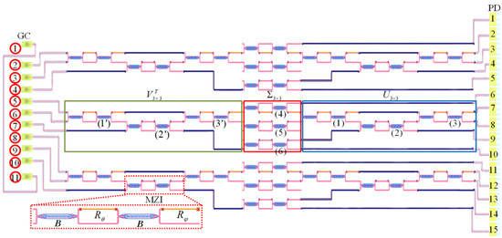
Figure 1.
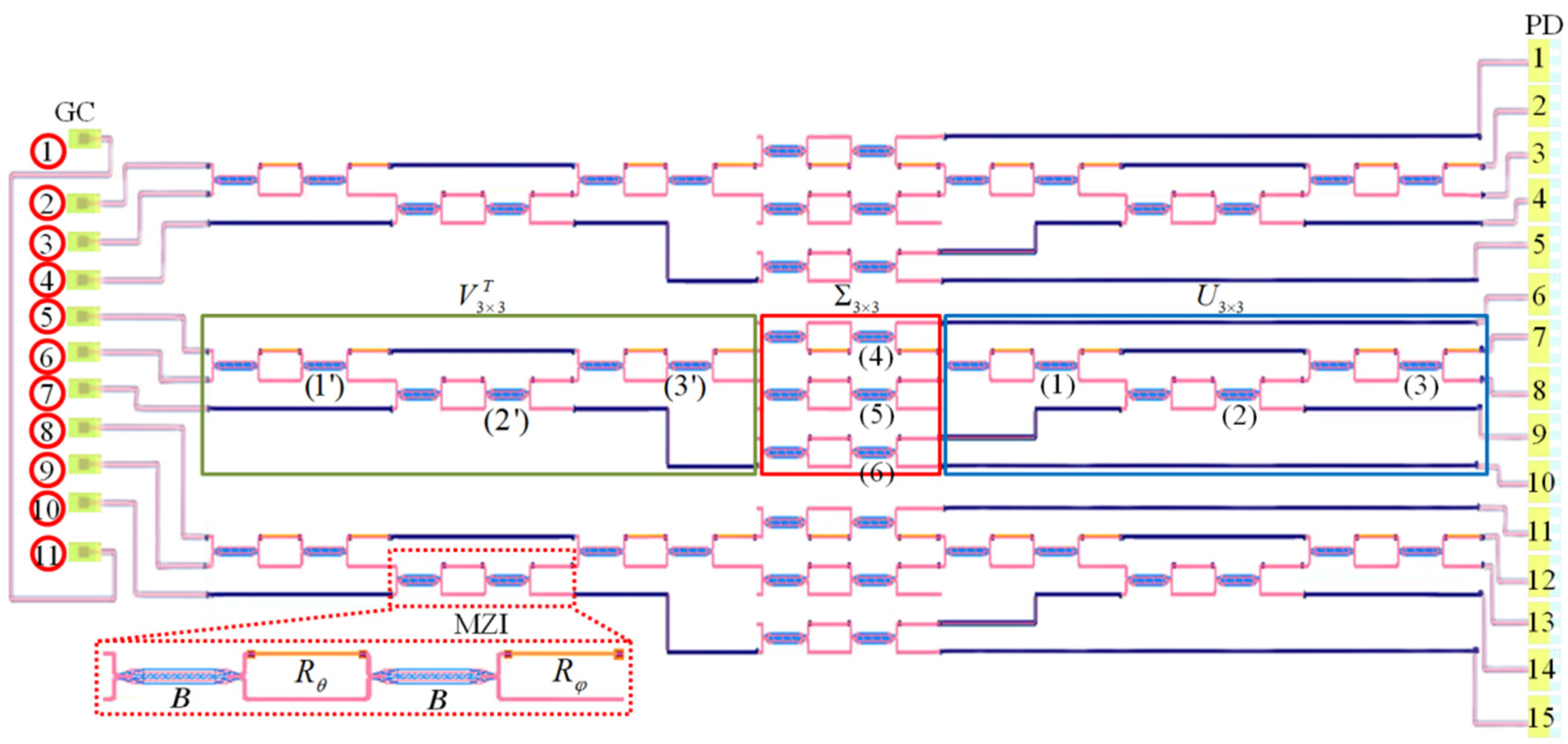
Illustration of three 3 × 3 MZI-based reconfigurable linear optical processors with nine input (GC 2 to 10) and fifteen output ports (PD 1 to 15). The SU (3) consists of MZIs labeled 1 to 3 (or 1′ to 3′). The section of the 3 × 3 structure comprises MZIs labeled 4 to 6.
We define the transmissivity and reflectivity of the MZI as
when θ = π, refle = 1, trans = 0 (MZI is on “bar-state (BS)”), and when θ = 0, refle = 0, trans = 1 (MZI in on “cross-state (CS)”). This MZI can implement any matrix in the special unitary group of degree two (i.e., SU (2)), composed of all complex square matrices whose conjugate transpose is equal to its inverse (unitary) and with a determinant equal to 1 (special unitary) [11].
The convolution kernel is a real-valued matrix. Real-valued matrix (M) may be decomposed by singular value decomposition (SVD) as
where U is an m × m unitary matrix, VT is the complex conjugate of the n × n unitary matrix V, Σ is an m × n diagonal matrix with non-negative-real numbers on the diagonal. Universal N-D unitary matrix can be implemented using a mesh of N (N − 1)/2 MZIs proposed by Reck et al. [12] or a mesh of N (N − 1)/2 proposed by Clements et al. [13]. Optical attenuators or optical amplification materials can be used to implement Σ [14]. Any N-D unitary matrix U can be decomposed into:
where (m, n) is a position and represents the rotation and translation operation of the U matrix’ m and n rows (or columns). Thus, S defines a specific ordered sequence. k is the serial number of MZI, D(γ1, γ2,…, γN) is a diagonal matrix with complex elements with a modulus equal to one on the diagonal. Matrix products for a sequence {O(k)} can be expressed:
T(k)m,n(θk, φk) can be expressed as:
We choose three 3 × 3 convolution kernels for each layer to implement CNN. Any 3 × 3 real-valued kernel (j = 1, 2, 3) can be illustrated:
Figure 1 depicts the schematic of the designed three 3 × 3 integrated reconfigurable linear processors. The structure comprises six SU (3) and three diagonal matrix multiplication for implementing three 3 × 3 kernels. As shown in Figure 1, the SU (3) contains the MZIs labeled 1 to 3 (or 1′ to 3′), constructing the unitary transformation matrix U3×3 (or ). While the middle section consists of MZIs labeled 4 to 6, implementing a non-unitary diagonal matrix . Eleven grating couplers (GCs) labeled 2 to 10 on the left side provide optical input ports. GCs labeled 1 and 11 are used for alignment testing during packaging. Fifteen PDs on the right side extract electrical signals from the chip. PD 1, PD 5, PD 6, PD 10, PD 11, and PD 15 are used to calibrate voltages of the internal phase shifters (θi) of MZIs.
4. Training and Simulation
The two-layer convolutional neural network is trained on the computer. The training progress is based on the abstract model of a CNN. Then, kernels obtained by training are converted into the MZIs’ phase in the photonic network. The abstract model’s input matrix, output matrix, and transmission matrix (kernel) correspond to the photonic network’s optical intensity signal (domain of optical powers). The transmission matrix (kernel) can be realized by controlling the output optical intensity of MZI. The output optical intensity of MZI is realized by changing phase shifters’ modulation voltage. We need to find a relationship between the modulation voltage and the output optical intensity of the MZI.
We used the INTERCONNECT (Ansys. Lumerical. Cor, V2020) to simulate the optical circuit. The basic parameters are set as follows:
- optical source: wavelength = 1550 nm; power = 27 mW; half-height width = 20 pm;
- detector: response wavelength = 1550 nm; and the dark current = 20 nA.
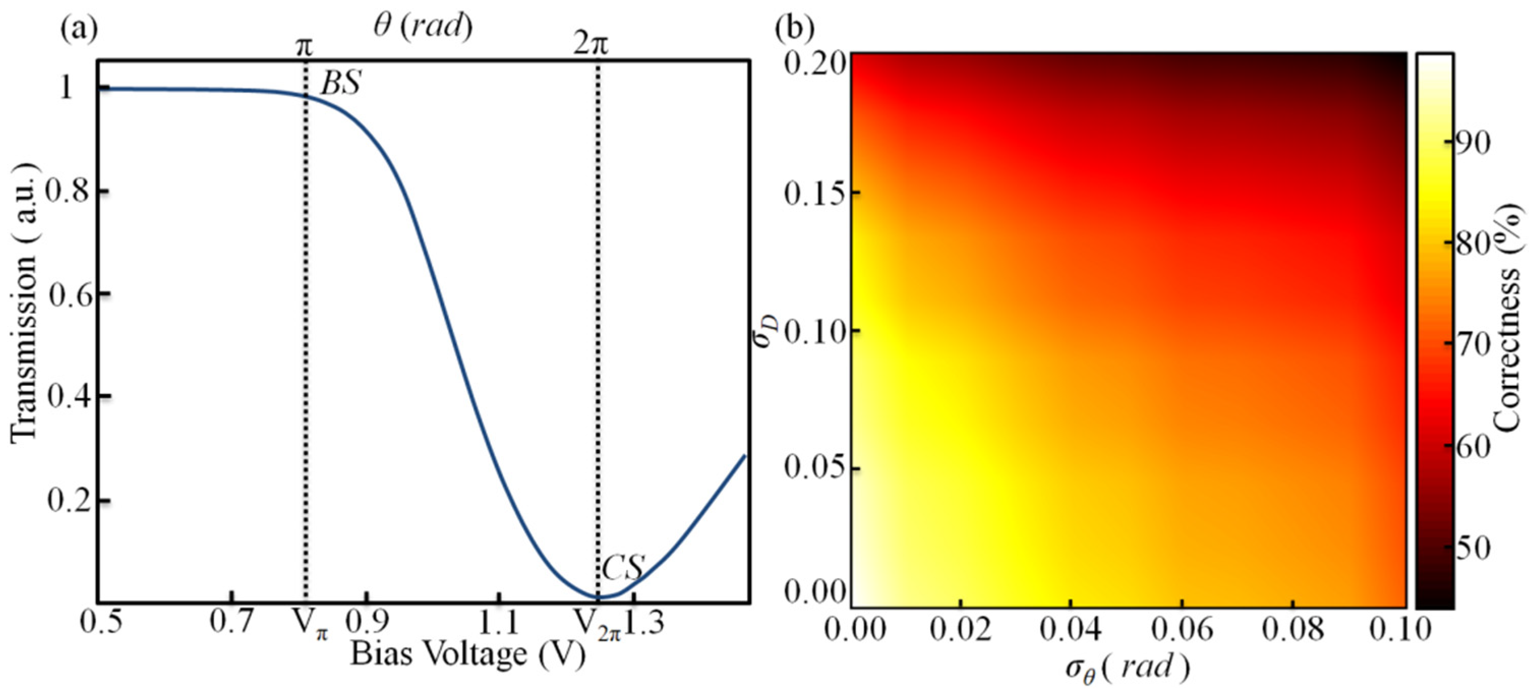
As shown in Figure 2a, the transmission of an MZI can be tuned by the voltage of the MZI’s internal phase shifter. The modulation voltage nearly has a linear relationship with the output optical intensity of MZI, when voltage = Vπ~V2π. Thus, the whole system works on this range.
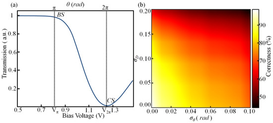
Figure 2.
(a) Simulated Bias Voltage VS optical power levels of a single MZI, where BS and CS represent PBS and PCS, respectively. (b) Classification accuracy for different phase standard deviations of the phase shifters σθ and PD error σD.
The phase errors σθ and the PD noises (σD) affect the classification accuracy of the two-layer CNN implemented by the optical processor. Here, the classification accuracy of the network is simulated with different σθ and σD. As shown in Figure 2b, the classification accuracy of the network achieved 98%, when σθ ≤ 0.01 (yellow region) and σD ≤ 0.025. The phase error σθ = 0.01 corresponds to an 8-bit modulation accuracy of the phase modulation voltage, affected by the half-wave voltage VHalf (=V2π − Vπ). PD error σD generally originates from the dark current. Here, σD = 0.025 corresponds to 25 nA dark current.
5. Experimental
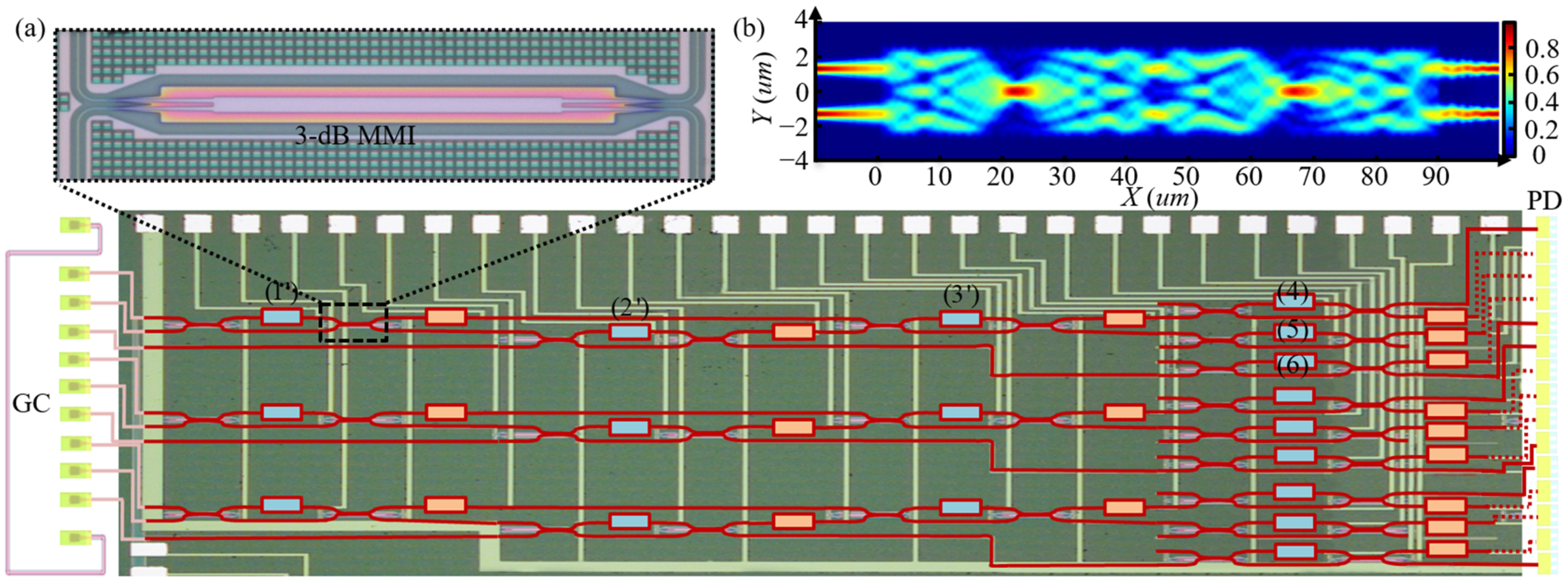
The device in this work operates at a wavelength of 1550 nm and fabricates on an SOI substrate with 220 nm × 450 nm cross-section. As mentioned above, the reconfigurable MZI-based optical processor is a mesh of tunable MZIs with 2 × 2 ports. Each MZI has two heater-based phase shifters Rθ and Rφ, which control the output power and two MZI outputs relative phase, respectively. To reduce the loss and enhance the robustness of the device against processing errors, MZI’s beam splitter adopts a 3 dB multimode interference (MMI). The relationship between the split ratio and MMI structure is simulated by FDTD (Ansys. Lumerical. Cor, V2020) through adjusting the coupler length, the coupler width, and the taper width. As shown in Figure 3b, the 3 dB coupler is achieved (the two output ports’ optical intensity are equal and maximum), when the coupler width equals 5.1 um, the taper width equals 1.3 um, and the coupling length equals 45 um or 90 um. Considering the processing error, the coupler length is set to be 90 um. Every MZI has 66 µm wide and 672 µm long, with two identical 150 µm heaters. The device can be reconfigured by applying voltages to the phase shifters, and electrical pads connect DC voltages and heaters. A fiber array with eleven ports couples vertically to the grating couplers. Fifteen PDs are silicon-doped lateral PIN Ge PD on the right side. Three 3×3 kernels have been realized in a silicon photonic platform through multi project wafer (MPW) in CUMEC (China Cor) [15]. Figure 3a depicts a microscope image of three VT3×3 parts and three parts of three 3 × 3 reconfigurable linear optical processors. This device has a total of 27 thermo-optic phase shifters connected to electrical pads, where 18 of them belong to VT3×3 and 9 of them for realizing ∑3×3. The chip has been packaged, and all electrical pads have been wire bonded.

Figure 3.
(a) Microscope image of the fabricated three 3 × 3 MZI-based reconfigurable linear optical processors. Inset shows one of MMI with a 3 dB split ratio. MZIs labeled 1′ to 3′ implement the unitary transformation matrix . MZIs labeled 4 to 6 construct . (b) The simulated electric field distribution of MMI.
To program the device experimentally, it is essential to determine the required DC voltages of every phase shifter. Exact accuracy on controlling phase shift is challenging in the experiment due to several error sources, including voltage fluctuations, the thermal crosstalk between MZIs, and fabrication process variations. Here, internal phase shifters (θi) of MZIs are analyzed mainly, which control the optical power splitting ratio (transmission) at the outputs of MZIs. For the external phase shifters with φi, an optical vector analyzer can be used to determine the required DC voltages directly [5]. Thus, before programming the device for a given application, θi of all MZIs must be calibrated first [16,17].
Figure 4 illustrates the schematic of the experimental setup. Here, a tunable laser generates continuous light (1550 nm, 27 mW). The optical signal is split into nine channels using four 1 × 3 optical splitters. The optical signal in each channel passes through a variable optical attenuator (VOA) which regulates the presence or absence of the input optical signal. DC voltage controlling unit (VCU) supplies modulated voltage of MZIs. PD is connected to the semiconductor analyzer (SA), with a constant bias voltage of 1 V.
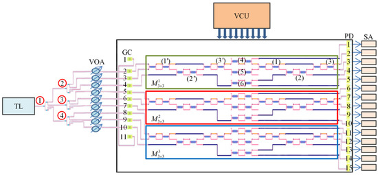
Figure 4.
Schematic of the experimental setup for the calibration process. TL: tunable laser (1550 nm, 27 mw); VOA: variable optical attenuators; VCU: voltage controlling unit; SA: semiconductor analyzer.
The calibration scheme is based on the topology of the SU (3), choosing the simplest path for each MZI. It starts from MZI (2′) and MZI (6) on the path GC4-PD5 of the structure shown in Figure 4. The configuration of MZI (2′) in its BS and MZI (6) in its CS allows for calibrating MZIs (2) and (3) on the paths GC4-PD4 and GC4-PD3. The configuration of MZI (2′) in its CS allows for calibrating MZIs (3′) and (4) on the path GC4-PD1. We configure MZI (1) by setting MZIs (2′), (3′), (4), and (3), which are previously configured to the required states on the path GC4-PD2. At this point, it is also possible to configure MZI (5) by setting MZIs (2′), (3′), (1), and (3), which are previously configured to the required states on the path GC4-PD2. Then, we calibrate MZIs (1′) on the path GC2-PD1. Eventually, MZIs in and are configured similarly. These calibrated parameters are shown in Table 3, Table 4 and Table 5.
Table 3.
Measured parameters through the experiment configuration of the MZIs in .
Table 4.
Measured parameters through the experiment configuration of the MZIs in .
Table 5.
Measured parameters through the experiment configuration of the MZIs in .
In the classification experiment, VOAs are used to adjust the input optical signal amplitude based on the MNIST handwritten digital test datasets and Fashion-MNIST test datasets. Simultaneously, convolutional kennels are deployed in the experiment based on parameters in Table 3, Table 4 and Table 5.
6. Results and Discussion
The calibration process is carried out from the beginning MZI to the end MZI. Figure 5 shows the ER1 of 10.54 dB, the bias voltage (VCS,1′) of 2.21 V, and the half-wave voltage (VHalf,1′) of 0.88 V of MZI (1′) in M 13×3. Here, ERi (= PBS,i − PCS,i) represents the extinction ratio of the MZI (i), where PBS,i is the transmitted optical power of MZI (i) in BS, and PCS,i is the transmitted optical power of MZI (i) in CS. The heaters exhibited a Pπ,1′ (i.e., the power for a π phase shift of MZI (1′)) of 8.43 mW with 553 Ω resistance. Table 3, Table 4 and Table 5 list the corresponding bias voltages (VCS,i) and the half-wave voltage (VHalf,i), PBS,i, PCS,i, ERi, Pπ,i of the phase shifters θi of the MZIs in . These parameters of MZI can be used in the following experiment.
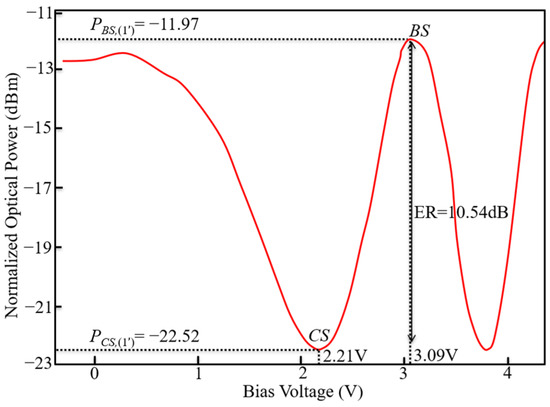
Figure 5.
The measured optical power of a single MZI (1′) in vs. the bias voltage.
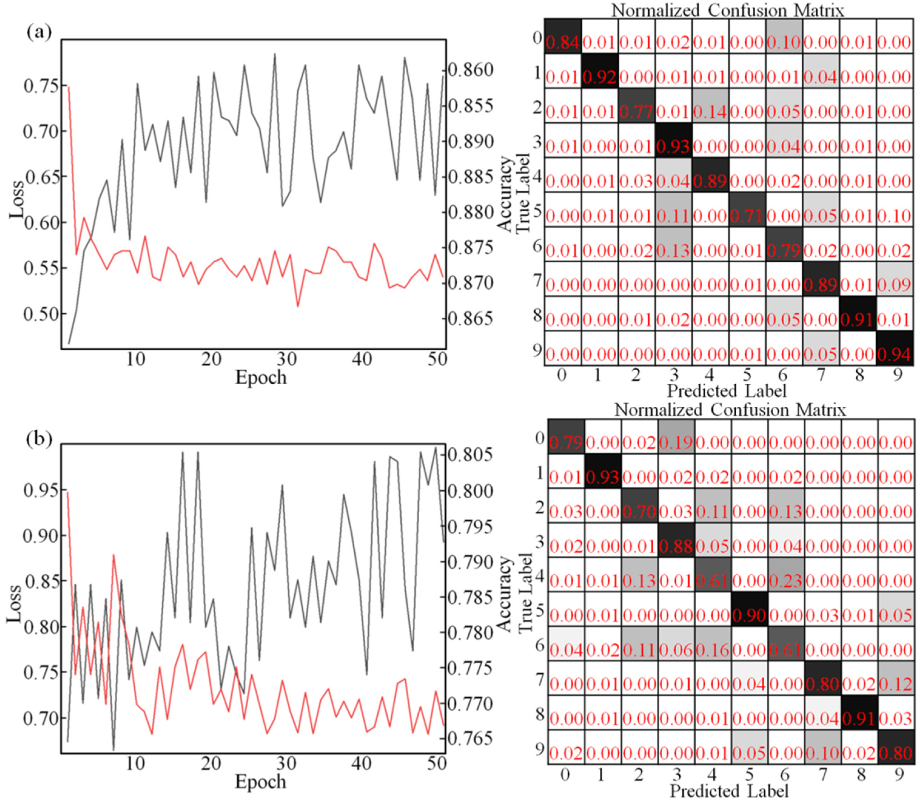
The classification experimental results of the optical processor (implement a two-layer CNN) are shown in Figure 6. It shows that the classification accuracy of MNIST datasets achieves 86.9%, and the classification accuracy of Fashion-MNIST datasets achieves 79.3%. The classification accuracy for each label in these datasets is different. As MNIST datasets (as shown in Figure 6a), the accuracy of label 1, label 3, label 8, and label 9 are higher than 90%. The classification ability of label 5 is slightly worse, with accuracy rates of 71%. Due to label 3, label 5, and label 7 being similar, the model misclassifies label 5 into other labels. As Fashion-MNIST datasets (as shown in Figure 6b), the accuracy of label 1, label 5, and label 8 is higher than 90%. The classification ability of label 4 and label 6 is slightly worse.
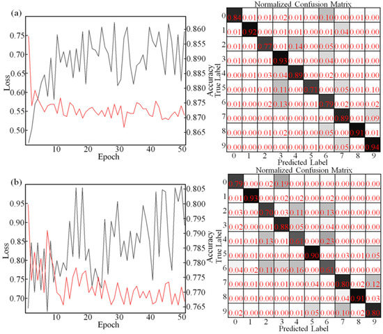
Figure 6.
(a) Accuracy rate and confusion matrix of the PHNN for the MNIST datasets. (b) Accuracy rate and confusion matrix of the PHNN for the Fashion-MNIST datasets.
As shown in Figure 2a, the classification accuracy of MNIST datasets retains about 94.7%, when σθ ≤ 0.01 rad and σD ≤ 0.01. In this work, the precision of VCU is 10 mV and the PD’s dark current is 20 nA. A phase shifter’s less than 10 mV voltage inaccuracy corresponds to a phase deviation of approximately 0.037 rad. For σθ ≥ 0.01 rad, the precision of the voltage regulators must be higher than 3.24 mV. The PD’s dark current is 20 nA, corresponding to σD ≈ 0.02. Moreover, the degradation in the classification accuracy is also attributed to MZIs’ thermal crosstalk. The external temperature control (ETC) platform is used to minimize the error caused by thermal crosstalk in the experiment. As reported in Reference [18], the error originating from the thermal crosstalk can be eliminated by using an n doping cross-section.
We compare devices in terms of several features for photonic analog processors. These features include network types, platforms, footprint, datasets, method, classification accuracy, central wavelength, and phase shifter power consumption (estimated through average Pπ). Table 6 illustrates these features on the reconfigurable linear optical processors. For a proper comparison, the table also lists the values taken from other MZI-based reconfigurable chips.
Table 6.
Comparison of the linear optical processors with MZI-based reconfigurable chips in the literature. DNN: deep neural networks.
7. Conclusions
In this paper, three 3 × 3 MZI-based optical processor is investigated. It is proved that this optical processor can realize an arbitrary unitary matrix. We obtain the experimental modulation voltage corresponding to the required phase shifts in the calibration process. MNIST datasets and Fashion-MNIST datasets are used to verify the classification performance of the optical processors. The classification accuracy of MNIST datasets is 86.9%, and the classification accuracy of Fashion-MNIST datasets achieves 79.3%. The experimental results show that experimental and fabrication imperfections degrade the classification accuracy of the optical processor. In the future, the optical processor can be embedded in computer architecture as an accelerator for computing matrix multiplication.
Author Contributions
Conceptualization, L.Z.; methodology, X.X.; software, W.Z.; validation, L.L., and P.Y.; writing—original draft preparation, X.X.; writing—review and editing, L.Z. All authors have read and agreed to the published version of the manuscript.
Funding
This research was funded by the Programme of Introducing Talents of Discipline to Universities (D17021) and the National Natural Science Foundation of China (Grant No.61903042).
Conflicts of Interest
The authors declare no conflict of interest.
References
- Athale, R.A.; Collins, W.C. Optical matrix–matrix multiplier based on outer product decomposition. Appl. Opt. 1982, 21, 2089–2090. [Google Scholar] [CrossRef] [PubMed]
- Farhat, N.H.; Psaltis, D.; Prata, A.; Paek, E. Optical implementation of the Hopfield model. Appl. Opt. 1985, 24, 1469–1475. [Google Scholar] [CrossRef] [PubMed]
- Shen, Y.; Harris, N.C.; Skirlo, S.; Prabhu, M.; Baehr-Jones, T.; Hochberg, M.; Sun, X.; Zhao, S.; LaRochelle, H.; Englund, D.; et al. Deep learning with coherent nanophotonic circuits. Nat. Photon. 2017, 11, 441–446. [Google Scholar] [CrossRef]
- Bagherian, H.; Skirlo, S.; Shen, Y.; Meng, H.; Ceperic, V.; Soljacic, M. On-Chip Optical Convolutional Neural Networks. arXiv 2018, arXiv:1808.03303. [Google Scholar]
- Shokraneh, F.; Geoffroy-Gagnon, S.; Nezami, M.S.; Liboiron-Ladouceur, O. A Single Layer Neural Network Implemented by a 4 × 4 MZI-Based Optical Processor. Phot. J. 2019, 11, 4501612. [Google Scholar] [CrossRef]
- Nahmias, M.A.; Lima, T.F.; Tait, A.N.; Peng, H.-T.; Shastri, B.J.; Prucnal, P.R. Photonic Multiply-Accumulate Operations for Neural Networks. IEEE J. Sel. Top. Quantum Electron. 2020, 26, 7701518. [Google Scholar] [CrossRef]
- Marinis, L.D.; Cococcioni, M.; Liboiron-Ladouceur, O.; Contestabile, G. Photonic Integrated Reconfigurable Linear Processors as Neural Network Accelerators. Appl. Sci. 2021, 11, 6232. [Google Scholar] [CrossRef]
- Xu, X.; Zhu, L.; Zhuang, W.; Zhang, D.; Yuan, P.; Lu, L. Photoelectric hybrid convolution neural network with coherent nanophotonic circuits. Opt. Eng. 2021, 60, 117106. [Google Scholar] [CrossRef]
- Hinton, G.E.; Salakhutdinov, R.R. Reducing the dimensionality of data with neural networks. Science 2006, 313, 504–507. [Google Scholar] [CrossRef] [PubMed] [Green Version]
- LeCun, Y.; Bottou, L.; Bengio, Y.; Haffner, P. Gradient-based learning applied to document recognition. Proc. IEEE 1998, 86, 2278–2324. [Google Scholar] [CrossRef] [Green Version]
- Genz, A. Methods for generating random orthogonal matrices. In Monte Carlo and Quasi-Monte Carlo Methods; Springer: Berlin/Heidelberg, Germany, 1998; p. 199. [Google Scholar]
- Reck, M.; Zeilinger, A.; Bernstein, H.J.; Bertani, P. Experimental realization of any discrete unitary operator. Phys. Rev. Lett. 1994, 73, 58–61. [Google Scholar] [CrossRef] [PubMed]
- Clements, W.R.; Humphreys, P.C.; Metcalf, B.J.; Steven, K.W.; Walsmley, I.A. An Optimal Design for Universal Multiport Interferometers. Optica 2016, 3, 1460–1465. [Google Scholar] [CrossRef]
- Connelly, M.J. Semiconductor Optical Amplifiers; Springer Science & Business Media: Berlin/Heidelberg, Germany, 2007. [Google Scholar]
- Liu, S.; Tian, Y.; Lu, Y.; Feng, J. Comparison of thermo-optic phase-shifters implemented on CUMEC silicon photonics platform. Int. Soc. Opt. Photonics 2021, 11763, 1176374. [Google Scholar]
- Miller, D.A.B. Self-aligning universal beam coupler. Opt. Exp. 2013, 21, 6360–6370. [Google Scholar] [CrossRef] [PubMed] [Green Version]
- Miller, D.A.B. Self-configuring universal linear optical component. Photon. Res. 2013, 1, 1–15. [Google Scholar] [CrossRef] [Green Version]
- Jayatilleka, H.; Shoman, H.; Chrostowski, L.; Shekhar, S. Photoconductive heaters enable control of large-scale silicon photonic ring resonator circuits. Optica 2019, 6, 84–91. [Google Scholar] [CrossRef] [Green Version]


Publisher’s Note: MDPI stays neutral with regard to jurisdictional claims in published maps and institutional affiliations. |
© 2022 by the authors. Licensee MDPI, Basel, Switzerland. This article is an open access article distributed under the terms and conditions of the Creative Commons Attribution (CC BY) license (https://creativecommons.org/licenses/by/4.0/).