Abstract
A two-dimensional ultrafast X-ray imager (UXI) composed of a time-dilation device, an electron-beam imaging unit, a gated microchannel plate (MCP) framing tube, and a pulser was developed. The time-dilation device extends the time spread of the electron signal generated by the pulsed photocathode (PC), and the electron-beam imaging unit images the electron pulse from PC to MCP. Finally, the gated MCP framing tube samples the dilated electron pulse. The time resolution and image size of the UXI were measured with an X-ray generated by a terawatt laser targeting device. When a driving pulse with a 2 V/ps slope is applied to the PC, the measured time resolution is 21 ps, and the image size is 12 mm × 3.9 mm. Furthermore, the image size varies with the time resolution. The results show that as the time resolution improves, the image size decreases. The use of two opposite-transmission PC driving pulses could improve the image size. Moreover, the measured UXI spatial resolution is 5 lp/mm, and the spatial resolution will be worse with the increasing off-axis distance.
1. Introduction
The gated MCP X-ray imager (GMXI) has two-dimensional spatial resolution and a high time resolution. It is a useful ultrafast diagnostic instrument for measuring hot spot nonuniformity or target implosion symmetry in inertial confinement fusion (ICF) experiments [1,2,3,4,5]. The measured results are critical for determining the hot spot pressure [6]. The imager uses gated MCP technology to achieve a time resolution of 35 to 100 ps [7,8]. When a sufficient voltage is applied to the MCP, it functions as a channel electron multiplier. In the GMXI, the MCP is driven by an ultrashort electric pulse. Therefore, photoelectrons converted from incident photons are sampled in ultrashort times, which results in a high time resolution. However, this imager is not fast enough to accurately measure ultrafast processes such as X-ray emission “hotspots”. For that hotspot, the distribution within 100 ps time is needed to be investigated, thus requiring time resolution better than 30 ps [9]. Therefore, a faster imager is required to detect these interactions. More recently, time-dilation technology was introduced into the GMXI. A dilation X-ray imager (DIXI) was successfully developed, and its time resolution was improved to 5 ps [4,10,11]. In the DIXI, the incident signal is first time dilated, and then the temporally magnified electron signal is sampled by a GMXI. Because the electron pulse arriving at the MCP has a much longer time duration than the incident signal, the DIXI time resolution is greatly improved. The DIXI dilates the electron signal by passing a driving pulse to the transmission PC. Therefore, a time-dependent electric field between the pulsed PC and the grounded anode mesh is achieved. The electrons emitted from the PC at different times can be accelerated with different electric fields. The earlier electrons travel faster than the later electrons. Subsequently, the electrons enter the drift region, which is an area from the mesh to the MCP with a 50 cm axial length. The electron signal is gradually temporally magnified until it reaches the MCP [4].
In this paper, a UXI is presented, with measurements performed by a terawatt laser targeting device. The differences between our UXI and Hilsabeck’s DIXI include the electron imaging system and the time resolution measurement method. In the DIXI, the electron imaging system used to image electrons from the PC to the MCP consisted of four solenoid magnet coils without soft iron. Coils with large excitation currents are used to generate a 370 Gauss uniform axial magnetic field, which achieves a spatial resolution of approximately 510 μm for gold PCs with 3 image demagnifications [5]. However, the large excitation current may cause a large Joule heat. The pulsed excitation current could be used to reduce the Joule heat. A pulse with a duration of ~1–10 ms and a peak current of ~1 kA was successfully used to excite magnet coils by Engelhorn et al. [9]. In the UXI, two short magnetic lenses with soft iron frames were used to generate an axisymmetric nonuniform magnetic field. The electrons from the PC to the MCP are imaged with a 2:1 image ratio. A spatial resolution of 5 lp/mm for the UXI is achieved. Short magnetic lenses have been frequently applied in streak cameras and electron microscopes to improve the optical-electronic imaging quality or focusing ability [12,13,14]. The short magnetic lens is excited by a small current to achieve a high spatial resolution, which reduces the Joule heat. However, short magnetic lenses have a disadvantage: the spatial resolution uniformity. The spatial resolution worsens as the distance between the photoelectron emission point and the PC center increases. Four or more magnetic lenses with larger diameter will be formed in our next generation electron-beam imaging system to improve the PC edge spatial resolution. Another difference is the time resolution measurement method. In the DIXI, the time resolution was measured by a Mach–Zehnder interferometer. The interferometer output two laser pulses, one of which was passed through an aperture in the shape of a vertical arrow, and then generated a vertical arrow image. The other one produced a horizontal arrow image. The horizontal arrow was fixed, and its arrival time was set in the center of the DIXI gating time interval. The arrival time of the vertical arrow was varied by adjusting its optical path length. The temporal adjustment for the vertical arrow appeared is ~5 ps, which demonstrated that the DIXI had a 5-ps time resolution [4]. Here, the UXI time resolution was acquired by an X-ray single shot, and the frame size of such dilation imager was discussed.
2. UXI Description
The UXI is made up of a time-dilation device, an electron-beam imaging unit, a gated MCP framing tube, and a pulser, as shown in Figure 1. The time-dilation device has three PCs, an anode mesh, and a drift region. The transmission X-ray PCs were achieved by coating 80 nm Au on a 90-mm-diameter C8H8 film. Each PC has a width of 12 mm and a 10 mm gap to the neighboring PC. The PC driving pulse output from the pulser is first connected to the input side connector by a coaxial cable and then guided to the PC with a copper tapered microstrip line. The tapered microstrip line is also used on the output side to prevent the driving pulse from reflecting back to the PC. A thin piece of gold is utilized to connect the tapered microstrip line to the PC. A 10 lp/mm anode mesh with ground potential is mounted 1.8 mm from PC. In addition to the driving pulse, a high negative DC bias voltage is applied to the PC. Therefore, a time-dependent electric field from the mesh to the PC is achieved. Electrons produced at different times can obtain different energies, resulting in electron speed spread. A schematic diagram of the driving pulse transmission along the PC and a photograph of the PCs are shown in Figure 2. The driving pulse is a traveling wave from left to right across the PC, and each photoelectron emission point in the PC experiences a time-dependent voltage. For instance, the driving pulse voltage at point A in the PC is A1 at time t1 and A2 at time t2. When voltage A2 is larger than voltage A1, a decreasing electric field is obtained, and the electron that was emitted earlier has a higher speed. The time length of the electron pulse is amplified as it travels in the 50 cm drift region.

Figure 1.
(a) UXI schematic diagram; (b) UXI (as shown in the red box) mounted on the target chamber.
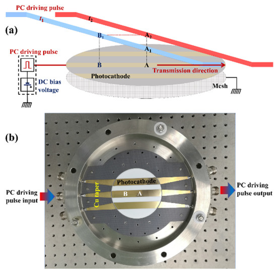
Figure 2.
(a) Schematic diagram of the driving pulse transmission along the PC. (b) Photograph of the transmission PCs.
The electrons are spatially dispersed in the 50 cm drift region. To achieve a high spatial resolution, an electron-beam imaging unit is employed. The electrons are imaged from the PC to the MCP with a 2:1 image ratio by the imaging unit, which consists of 2 annular magnetic lenses. Each magnetic lens consists of a 1320-turn copper coil and a soft iron frame. The axial length, inner diameter, and outer diameter of the lens are 100 mm, 160 mm, and 256 mm, respectively. In the inner circumference center, a circular slit with a 4 mm width is used for the magnetic field leaking from the soft iron to the drift region to image the electron pulse. The lenses are mounted in the drift region. The distance between the center of the first lens and the PC is 12.5 cm, while the distance between the center of the second lens and the MCP is 9 cm. The currents in the copper coils are 0.198 A and 0.31 A, resulting in an axially symmetric nonuniform magnetic field.
The magnified electron pulse is imaged in the MCP and sampled by the time-resolved gated MCP framing tube. The framing tube consists of an MCP, as well as a phosphor screen. The MCP has a diameter of 56 mm, a thickness of 0.5 mm, a channel diameter of 12 μm, and a bias angle of 6°. The MCP input surface formed by depositing a copper layer over a gold layer on three microstrip lines. The gold and copper films are also coated on the MCP output surface, which are successively deposited on the whole surface and connected to the ground. Each MCP microstrip line has an 8 mm width and a 3 mm gap with the adjacent line. The phosphor is applied with a +4 kV DC high voltage and placed 0.5 mm from the MCP. In general, the opening voltage at which the MCP produces the lowest amplification sufficient to generate the output charge is approximately 600 V, as below that voltage the incoming electrons are absorbed inside the pores. When a sufficient voltage greater than the opening voltage is applied to the MCP, the electrons entering the MCP channel are multiplied. At this time, the MCP is a channel electron multiplier. When the electric potential difference between the MCP input surface and MCP output surface is less than the opening voltage, the electrons entering the MCP channel are absorbed, and there is no signal output from the MCP. The MCP is usually only applied with a DC bias voltage that is less than the MCP opening voltage. Therefore, the MCP is turned off most of the time. While an ultrashort electric pulse drives MCP, the MCP total voltage is the sum of the time-dependent pulse voltage and the DC bias. The MCP turns on when the MCP total voltage is greater than the opening voltage. Because of the ultrashort duration of the electric pulse, the MCP turn-on time is ultrashort, which results in a high time resolution for the gated MCP framing tube. A schematic diagram of the ultrashort pulse transmission along the MCP is shown in Figure 3. An ultrashort pulse travels from one side of the MCP microstrip transmission line to the other, with each point on the MCP microstrip transmission line receiving a time varying voltage. For instance, point O on the MCP is applied with voltage O1 at time and voltage O2 at time . The electrons arriving at point O will be gained when the MCP total voltage exceeds the opening voltage. When the magnified electron signal is synchronized with the ultrashort pulse, the electron signal is sampled and multiplied by the MCP. The electric field from the phosphor to the MCP accelerates the multiplied electrons, which then impact the phosphor and convert to fluorescence. A CCD is used to collect the fluorescence.
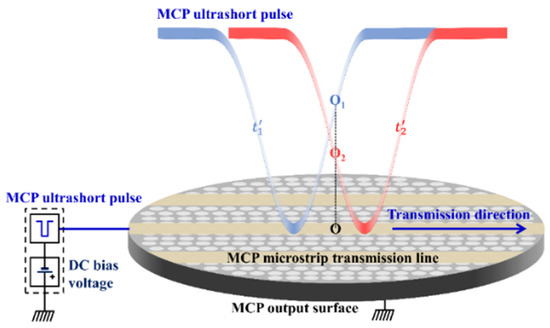
Figure 3.
Schematic diagram of the ultrashort pulse transmission along the MCP.
The pulser generates both the PC driving pulse and the MCP ultrashort pulse, and it is made up of an avalanche transistor circuit and a diode shaper. First, avalanche transistor stacks are connected to a Marx bank circuit to produce six fast step pulses. Three of these pulses are used to excite the PCs, while the other three are separately shaped by an avalanche diode to produce three MCP ultrashort pulses [15]. The PC driving pulses have a slope of approximately 2 V/ps. In addition, the MCP ultrashort pulses are achieved with widths of 225 ps and amplitudes of −1.8 kV.
In the limit of a small accelerating gap between the PC and the anode mesh, neglecting the birth energy dispersion, the electron that enters the drift region at time ti will arrive at the MCP at the following time [4,10]:
Here, L is the drift length of 50 cm; e and m are the electron charge and mass, respectively; and is the potential difference between the PC and the anode mesh when the photoelectron is produced at time t, where is the −3 kV PC bias voltage and is the 2 V/ps PC driving pulse slope. The temporal magnified factor M between two time steps is as follows:
Then, the UXI time resolution can be given by [10]:
where TMCP is the gate width of the MCP framing tube.
As the driving pulse travels in the PC, the photoelectron emitted points along the PC have varying voltages. For instance, in addition to the negative high DC bias voltage, point A in the PC receives voltage A1 and point B receives voltage B1 at time t1, as shown in Figure 2a. Voltage B1 is larger than voltage A1, which leads to a faster speed for photoelectrons emitted from A than from B. Therefore, the drift time from the mesh to the MCP for the photoelectrons from A is less than that of the photoelectrons from B. Because the MCP has a gate width of TMCP, the drift time difference of the photoelectrons should be less than TMCP to ensure that the photoelectrons are received at the same time. Otherwise, one of the photoelectrons emitted from A and B will be gained, while the other will be absorbed. It is assumed that the PC driving pulse takes time t to be transmitted from B to A, and the drift time difference between photoelectrons from A and B is:
Formula (6) shows that the maximum distance between points A and B is , which ensures that the photoelectrons emitted from A and B are imaged at the same time. Here, is the transmission speed of the driving pulse in the PC. That is, the frame size of the UXI image along the PC is:
3. Measurement Results
The UXI measurements were performed by a terawatt laser targeting device, and the measurement setup is shown in Figure 4. The terawatt laser was produced by Amplitude Systemes Company. The laser system outputs two laser pulses with wavelengths of 390 and 780 nm and pulse widths of 100 fs. The 780 nm laser with an energy of 650 mJ is first reflected by mirrors M2 and M3 and then hits an iron planar target to generate X-rays. The UXI was placed outside the target chamber, and the PC was 71 cm from the iron target. There is no component between the iron target and the PC. Therefore, the X-rays can irradiate the unobstructed PC to generate photoelectrons. The 390 nm laser is reflected from a total reflector M1 to a positive-intrinsic-negative (PIN) diode, producing an electric signal that serves as a trigger signal for the pulser to produce the driving pulse in the PC and the ultrashort pulse in the MCP. To ensure that the X-rays were synchronized with the PC driving pulse, a DG535 was used as the delay circuit and was utilized to precisely adjust the trigger time. Then, the photoelectrons were accelerated by the varied electric field, resulting in an electron velocity dispersion that increases the time duration of the electron signal. Finally, the ultrashort pulse was timed to sample the magnified electron pulse in the MCP, and a gating image with time dilation was obtained.
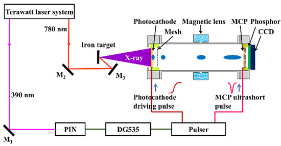
Figure 4.
UXI performance measurement experimental device.
A static image is obtained with a −3 kV static DC bias for the PC and a −700 V bias for the MCP, as shown in Figure 5a. The intensity distribution in Figure 5a is not uniform, which is because of the nonuniform spatial distribution of the X-rays due to the bad laser mode. A gating image with time dilation is shown in Figure 5b, when the PC is given a driving pulse in addition to the −3 kV DC bias and the MCP is given an ultrashort pulse in addition to the −500 V DC bias. To obtain X-ray information with different times, three coaxial cables with equal difference in length are used. The coaxial cable length is increased by a 10 mm step. Then, the three PC driving pulses reach the PCs at different times. The delay time between each pair of adjacent PC driving pulses is about 50 ps. In this experiment, the driving pulse on the middle transmission PC is synchronized with the X-ray pulse, while the other two PCs are unsynchronized. Therefore, a gating image is only obtained in the middle PC. The intensity versus the spatial distribution along the MCP from Figure 5b is shown in Figure 6a. The final results in Figure 6a are calibrated by the static results from Figure 5a. Because of the 2:1 image ratio, the PC area related to the gating image is doubled. The driving pulse travels left to right across the PC at a velocity of approximately 1.87 × 10⁸ m/s. The intensity versus temporal distribution along the PC for the gating image was obtained from the PC driving pulse velocity and the gating image spatial distribution, as shown in Figure 6b. As analyzed in Formula (7), the time resolution can be obtained from the PC streak image. The full width at half maximum (FWHM) of the temporal distribution curve represents the time resolution [5,7,8]. In Figure 6b, the black solid line and the red line represent the experimental results and the Gaussian fitting, respectively. Figure 6b shows that the time resolution of the UXI is 21 ps.
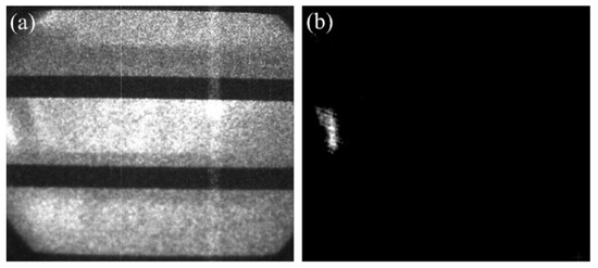
Figure 5.
(a) Static image, while the PC receives a static DC bias of −3 kV and the MCP receives a static DC bias of −700 V. (b) Gating image with time dilation, when a −3 kV DC bias and a driving pulse are applied to the PC, and an ultrashort pulse and a −500 V DC bias are applied to the MCP.
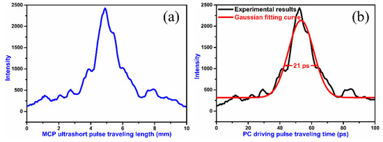
Figure 6.
(a) The intensity versus spatial distribution along the MCP, with signals from the image in Figure 5b. (b) The intensity versus time distribution along the PC.
From Figure 5b and Figure 6a, it can also be seen that the frame size of the UXI is 12 mm × 3.9 mm. The PC width determines the frame size perpendicular to the PC of 12 mm. The voltage spatial distribution of the driving pulse reduces the frame size along the PC to 3.9 mm. The voltage spatial distribution causes the electrons emitted from different positions along the PC to have varying drift times from the mesh to the MCP. Because of the time-resolved MCP, electrons with drift time differences less than the MCP gate width can be gained by the MCP to output the signal, while the remaining electrons are absorbed by the MCP. Therefore, the gating image with time dilation is a streak image, as shown in Figure 5b. In the ICF experiment, the object is first enlarged by the Kirkpatrick–Baez (KB) X-ray microscope or the pinhole array and then imaged in the PC [16]. The frame size is an important parameter that is closely related to the spatial resolution and the detectable object size [17]. A larger frame size allows for greater enlargement magnitudes, which improves the spatial resolution. While the enlargement magnitude is fixed, the detectable object size increases with the increasing frame size. Currently, each dimension of the frame size in frequently used X-ray imagers is 6–13 mm [17], and the 3.9 mm frame size along the PC is too small. The relationship between the theoretical UXI frame size along the PC and the time resolution is shown in Figure 7, with the frame size decreasing with improving time resolution.
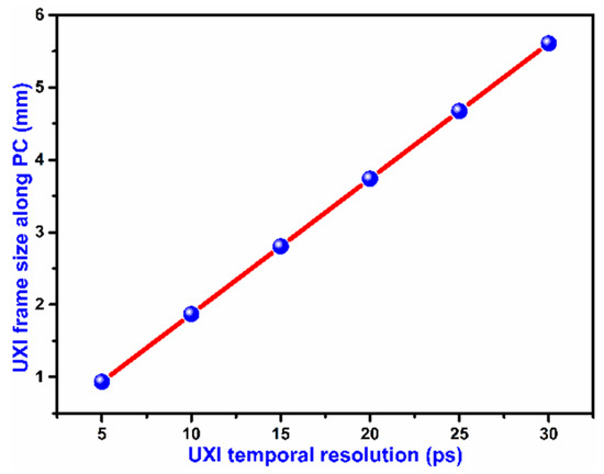
Figure 7.
The relationship between the theoretical UXI frame size along the PC and the time resolution.
To increase the UXI image size, two opposite-transmission driving pulses should be used to simultaneously excite the PC. Figure 8 shows the schematic diagram for this method. The first driving pulse travels from left to right across the PC, while the second pulse travels from right to left. At a certain time, the voltage at point C in the PC is equal to the voltage at point C1 in the first PC driving pulse plus the voltage at point C2 in the second PC driving pulse. It can be concluded from Figure 8 that the voltage at each point in the PC is consistent. Therefore, electrons emitted from different PC positions have the same drift times from the mesh to the MCP, and the UXI frame size is not limited by the time resolution, which allows for larger frame sizes. It should be noted that when the PC driving pulse was synchronized with the input optical signal, the PC driving pulse starting points S1 and S2 passed through the PC end points in their respective transmission directions.
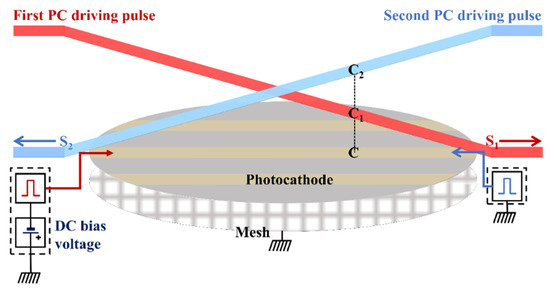
Figure 8.
Schematic diagram of two opposite-transmission driving pulses used to simultaneously excite the PC to increase the UXI image size.
In addition to the time resolution and frame size, the spatial resolution is also an important performance index for the UXI. The spatial resolution is mainly dependent on the MCP framing tube and the electron-beam imaging unit [9]. The spatial resolution of the MCP framing tube is influenced by the microchannel diameter, the distance between two neighboring microchannel pores, the length from the MCP to phosphor screen, and the applied voltage for the phosphor screen. The spatial resolution of the electron-beam imaging unit is provided by the magnetic field produced by the pair of annular magnetic lenses. The UXI spatial resolution is characterized using a resolution mask, which is deposited directly on a quartz substrate, and then 25 nm thick gold is coated on the resolution mask. There are different groups of slits in the mask to determine the best spatial resolution. The resolution mask including several 3 mm × 3 mm squares are formed by lots of regular slits, shown in Figure 9. The slits with 8 different spatial frequencies are achieved, which are 2, 5, 10, 15, 20, 25, 30 and 35 lp/mm. The slits are parallel or perpendicular to the PC transmission line, and the slits in two neighboring squares are perpendicular to each other. On the quartz substrate, the spatial resolution mask with 2 to 35 lp/mm is deposited repetitively along the PC transmission line. The UV light irradiates the whole PC plane to excite the photoelectron image. When the PC is applied with −3 kV, and the MCP is with −700 V, the middle PC image with resolution mask is shown in Figure 10a. The enlarged views of the mask with 2 lp/mm and 5 lp/mm in the middle PC image are shown in Figure 10b. It can be seen that the mask is gradually obscured with increasing off-axis distance. The relationship between the contrast ratio of 5 lp/mm mask and off-axis distance is shown in Figure 10c. The contrast ratio is reduced while the off-axis distance is increased. That is to say, the spatial resolution is worse with the increasing off-axis distance. Figure 10c shows that when the PC sensitive area has a diameter within 30 mm, the contrast ratio of the 5 lp/mm mask is better than 11%, which satisfies the Rayleigh resolution criterion of a valley to peak ratio of 0.81. Therefore, the limiting spatial resolution of UXI is 5 lp/mm, and the corresponding PC sensitive area is 30 mm in diameter.
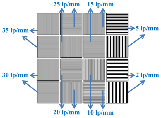
Figure 9.
Schematic diagram of the spatial resolution mask.
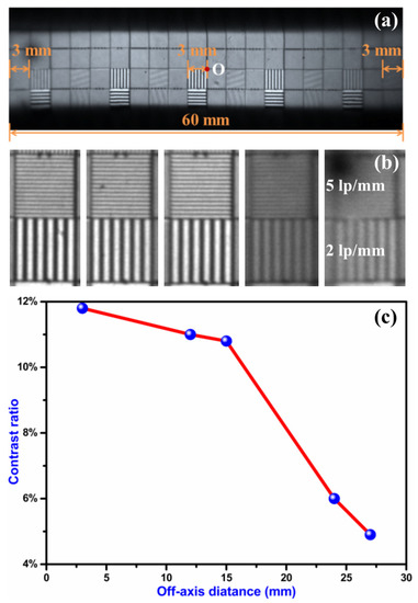
Figure 10.
(a) The middle PC image with resolution mask. (b) The enlarged views of the mask with 2 lp/mm and 5 lp/mm in the middle PC image. (c) The relationship between the contrast ratio of 5 lp/mm mask and off-axis distance.
4. Conclusions
A UXI with a 21-ps time resolution and 5-lp/mm spatial resolution was developed. The UXI improves the time resolution by sending a driving pulse through the PC to achieve a large time spread of the electron signal. However, the driving pulse leads to a voltage distribution along the PC, which results in electrons emitted from different PC positions having various drift times in the 50 cm drift region. Because of the time-resolved MCP, electrons with a drift time difference less than the MCP gate width can be gained by the MCP to output signal, while the remaining electrons are absorbed by the MCP and no signal is output. The UXI measurements were performed by a terawatt laser targeting device. When the PC receives both a driving pulse and a −3 kV DC bias and the MCP receives an ultrashort pulse and a −500 V DC bias, a PC streak image is achieved. Based on the PC streak temporal distribution curve, the time resolution and the frame size of the UXI are 21 ps and 12 mm × 3.9 mm, respectively. The voltage spatial distribution of the driving pulse along the PC causes the small frame size, and the frame size decreases with the improving time resolution. To increase the size of the UXI image, two opposite-transmission driving pulses should be used to excite the PC simultaneously.
Author Contributions
Investigation, H.C., K.L., Q.L., D.W., J.H., K.X., L.L. and J.L.; methodology, H.C.; writing—original draft, H.C.; writing—review and editing, H.C. All authors have read and agreed to the published version of the manuscript.
Funding
This research was funded by National Natural Science Foundation of China (NSFC), grant number 11775147; Guangdong Basic and Applied Basic Research Foundation, grant numbers 2019A1515011474 and 2019A1515110130; Shenzhen Science and Technology Program, grant numbers JCYJ20210324095007020, JCYJ20200109105201936, and JCYJ20190808115605501.
Conflicts of Interest
The authors declare no conflict of interest.
References
- Li, L.; Zhang, W.; Jing, L.; Du, H.; Zhang, L.; Zheng, J.; Li, H.; Lin, Z.; Zhan, X.; Yu, R.; et al. Optimization of tungsten-doped high density carbon target in inertial confinement fusion. Nucl. Fusion 2021, 61, 126023. [Google Scholar] [CrossRef]
- Baker, K.L.; Celliers, P.; Tabak, M.; Wallace, R.; Sorce, C.; Whiting, N.; Grim, G.; LeChien, K.; Avila, T.G.; Dolan, D.H.; et al. Converting existing optical detectors into fast X-ray detectors. Rev. Sci. Instrum. 2021, 92, 073507. [Google Scholar] [CrossRef] [PubMed]
- Li, S.; Wang, Q.; Yao, X.; Cao, Z.; Liu, J.; Zhao, Q. Two-dimensional time- and space-resolved diagnostic method for an integrated implosion process. Opt. Express 2021, 29, 33424–33433. [Google Scholar] [CrossRef] [PubMed]
- Hilsabeck, T.J.; Hares, J.D.; Kilkenny, J.D.; Bell, P.M.; Dymoke-Bradshaw, A.K.L.; Koch, J.A.; Celliers, P.M.; Bradley, D.K.; McCarville, T.; Pivovaroff, M.; et al. Pulse-dilation enhanced gated optical imager with 5 ps resolution. Rev. Sci. Instrum. 2010, 81, 10E317. [Google Scholar] [CrossRef] [PubMed]
- Nagel, S.R.; Hilsabeck, T.J.; Bell, P.M.; Bradley, D.K.; Ayers, M.J.; Barrios, M.A.; Felker, B.; Smith, R.F.; Collins, G.W.; Jones, O.S.; et al. Dilation x-ray imager a new/faster gated X-ray imager for the NIF. Rev. Sci. Instrum. 2012, 83, 10E116. [Google Scholar] [CrossRef] [PubMed]
- Theobald, W.; Sorce, C.; Bedzyk, M.; Ivancic, S.T.; Marshall, F.J.; Stoeck, C.; Shah, R.C.; Lawrie, M.; Regan, S.P.; Sangster, T.C.; et al. The single-line-of-sight, time-resolved X-ray imager diagnostic on OMEGA. Rev. Sci. Instrum. 2018, 89, 10G117. [Google Scholar] [CrossRef] [PubMed]
- Kilkenny, J.D. High speed proximity focused X-ray cameras. Laser Part. Beams 1991, 9, 49–69. [Google Scholar] [CrossRef]
- Bell, P.M.; Kilkenny, J.D.; Hanks, R.L.; Landen, O.L. Measurements with a 35 psec gate time microchannel plate camera. In Proceedings of the 34th Annual International Technical Symposium on Optical and Optoelectronic Applied Science and Engineering, San Diego, CA, USA, 8–13 July 1990; Volume 1346, pp. 456–464. [Google Scholar]
- Engelhorn, K.; Hilsabeck, T.J.; Kilkenny, J.; Morris, D.; Chung, T.M.; Dymoke-Bradshaw, A.; Hares, J.D.; Bell, P.; Bradley, D.; Carpenter, A.C.; et al. Sub-nanosecond single line-of-sight (SLOS) X-ray imagers. Rev. Sci. Instrum. 2018, 89, 10G123. [Google Scholar] [CrossRef] [PubMed]
- Nagel, S.R.; Hilsabeck, T.J.; Bell, P.M.; Bradley, D.K.; Ayers, M.J.; Piston, K.; Felker, B.; Kilkenny, J.D.; Chung, T.; Sammuli, B.; et al. Investigating high speed phenomena in laser plasma interactions using dilation X-ray imager. Rev. Sci. Instrum. 2014, 85, 11E504. [Google Scholar] [CrossRef] [PubMed]
- Cai, H.; Fu, W.; Bai, Y.; Lei, Y.; Liao, Y.; Liu, J. Simulation of a dilation X-ray framing camera. J. Electron. Imaging 2017, 26, 043003. [Google Scholar] [CrossRef]
- Feng, J.; Engelhorn, K.; Cho, B.I.; Lee, H.J.; Greaves, M.; Weber, C.P.; Falcone, R.W.; Padmore, H.A.; Heimann, P.A. A grazing incidence X-ray streak camera for ultrafast, single-shot measurements. Appl. Phys. Lett. 2010, 96, 134102. [Google Scholar] [CrossRef]
- Konvalina, I.; Müllerová, I. Properties of the cathode lens combined with a focusing magnetic/immersion-magnetic lens. Nucl. Instrum. Methods Phys. Res. Sect. A 2011, 645, 55–59. [Google Scholar] [CrossRef]
- Chang, Z.; Rundquist, A.; Zhou, J.; Murnane, M.M.; Kapteyn, H.C.; Liu, X.; Shan, B.; Liu, J.; Niu, L.; Gong, M.; et al. Demonstration of a sub-picosecond X-ray streak camera. Appl. Phys. Lett. 1996, 69, 133–135. [Google Scholar] [CrossRef]
- Bell, P.M.; Kilkenny, J.D.; Landen, O.L.; Hanks, R.L.; Bradley, D.K. Electrical characteristics of short pulse gated microchannel plate detectors. Rev. Sci. Instrum. 1992, 63, 5072–5074. [Google Scholar] [CrossRef]
- Li, Y.; Dong, J.; Xie, Q.; Xu, J.; Liu, H.; Li, W.; Wang, X.; Mu, B.; Wang, Z.; Chen, F.; et al. Development of a polar-view Kirkpatrick-Baez X-ray microscope for implosion asymmetry studies. Opt. Express 2019, 27, 8348. [Google Scholar] [CrossRef] [PubMed]
- Oertel, J.A.; Archuleta, T.; Bakeman, M.; Sanchez, P.; Sandoval, G.; Schrank, L.; Walsh, P. A large-format gated X-ray framing camera. In Proceedings of the Optical Science and Technology, SPIE’s 48th Annual Meeting, San Diego, CA, USA, 3–8 August 2003; Volume 5194, pp. 214–222. [Google Scholar]


Publisher’s Note: MDPI stays neutral with regard to jurisdictional claims in published maps and institutional affiliations. |
© 2022 by the authors. Licensee MDPI, Basel, Switzerland. This article is an open access article distributed under the terms and conditions of the Creative Commons Attribution (CC BY) license (https://creativecommons.org/licenses/by/4.0/).