Abstract
We propose a detailed method for the interconnection between optical fibers and waveguides of photonic integrated circuits. Appropriate modal transmission is accomplished by matching the mode field diameters from both waveguide structures. Links from one structure to another are created by an interconnecting waveguide, maintaining a fixed coupling efficiency as its size is modified to adjust to the target waveguide core. This tailored transition acts as a mode field adapter, equalizing the transmission among multiple modes and reducing the mode-dependent losses while coupling. We present an algorithm to design the mode field adapter based on matching the effective mode areas using the power overlap integral. A study case considering a polymer photonic integrated device immediately connected to a few-mode fiber is analyzed. Coupling efficiencies over 90% for every transmitted mode are achieved, showing an evident improvement compared to typical approaches only matching core sizes. Detailed comparison of the results for each transmission mode is presented. This same procedure can be used to interconnect optical waveguides with different refractive index profiles and core geometry.
1. Introduction
Photonic integrated systems have become a mature technology, showing huge potential for new alternatives in ultra-fast signal processing [1,2]. There is ongoing intensive research aiming to extend the number of devices working using this technology [3,4,5]. Specifically, in the field of optical telecommunications, a large amount of diverse applications already utilize systems and devices based on integrated photonics. The recent expansion of optical telecommunications has evolved in techniques such as mode division multiplexing (MDM) and space division multiplexing (SDM), aiming to increase the amount of data channels in a single link [6,7,8]. These techniques are based on using the multiple spatial modes available in optical waveguides as independent channels, rather than increasing the amount of physical waveguides. Thus, the use of photonic integrated systems has become a powerful tool to boost the capacity of telecommunication applications. Whereas there are multiple platforms and materials to fabricate integrated photonic systems, optical fibers are still the foremost option for signal transmission.
Interconnection between integrated devices and optical fibers is a crucial aspect to consider and address. Signal delivery in and out from photonic integrated circuits (PICs) is mainly achieved by approaching the fibers either at the edge or the top of the PIC [9,10]. The chosen approach depends on the material used for the fabrication of the PIC since each material must be processed with different techniques [11,12,13,14]. The development of single-mode signal coupling has been extensively investigated, resulting in diverse, highly efficient methods [15,16,17]. Nonetheless, the coupling of multimode signals between PICs and optical fibers still offers room for improvement. This is a fundamental aspect for the utilization of emerging MDM and SDM technologies. Recently, some works have reported alternatives to undertake the interconnection among multimode PICs and optical fibers [18,19]. With respect to optical fibers, different few-mode fibers (FMFs) able to transmit only a restricted number of spatial modes have been demonstrated and successfully tested for transmission applications [20]. The main requirement to consider for this type of interconnection is an optimized waveguide for the correct transmission of all the modes, preventing mode coupling among symmetrical and non-symmetrical modes.
For top coupling purposes, the most popular solution is to use gratings to scatter light and couple into the desired fiber core or integrated waveguide [19,21]. Although this type of coupling performs well with a minimum footprint, it requires high-resolution structures involving complex fabrication processes. In-plane or edge coupling is a more common technique since it can be done with less specialized fabrication processes, resulting in simpler structures [9,22,23]. This type of coupling includes the transition from dissimilar waveguide cores involving different spot sizes. Pairing of both waveguides is done either by using lens-based elements or tapered-waveguide connecting structures [18,24,25]. The latter includes the use of spot size converters or mode field adapters. Complications related to edge coupling using these structures arise from the long lengths, compromising the high integration of the systems and usually requiring side polishing of the PICs. Another approach relies on evanescent waves coupling light from one waveguide to another, requiring the use of tapered waveguides, which involves the same restraints in length [9].
One method to fabricate PICs and integrated devices consists of using the direct laser writing (DLW) technique. This technique consists of highly focusing a laser beam on a material and generating localized structural changes in the material. The most common approach to perform this technique consists of using a two-photon absorption effect using an infrared pulsed laser impinging on glasses, crystals or polymers [26,27,28]. As a result of this process, the material is locally modified, inducing a modification in the refractive index. Induced material modification follows a circular-like cross-section area, which usually results in a slight increase in refractive index. By this method, three-dimensional structures can be created on a surface or inside a volume, such as optical low-contrast waveguides or photonic devices. The DLW technique can also be used in photosensitive polymeric resins (photoresins), commonly used in photolithography processes [15]. Polymer-based photonic systems represent a cost-effective and uncomplicated option to create complex designs instead using semiconductors or different glasses [13,29]. The application of the DLW technique has been demonstrated to be able to create different structures from waveguides, mode field adapters and micro-lenses. A simpler and low-cost method alternative for using a pulsed laser with photoresins consists of using low-absorption wavelengths in the visible range and then creating 3D structures at micron or sub-micron scale [30]. Taking advantage of the adaptability of using the DLW fabrication technique, wire bonding processes have been developed for photonic device interconnection [31]. Following the same technique, complex and elaborated structures can be created, which potentially can be used to couple light from one device to another [22].
In this work, we present the guidelines and considerations for an alternative when creating interconnections of two different few-mode optical waveguides with low contrast index. We provide a set of guidelines to reduce the mode mismatch between both cores based on a waveguide interconnecting structure of non-conventional profile designed considering the optimal coupling for all the transmitted modes. Specifically, we focus on the interconnection between an optical few-mode fiber and a polymeric photonic integrated device with a circular cross-section core. In our results, we compare the coupling efficiency or mode-dependent losses (MDL) for the different transmitted modes compared with traditional structures. Our calculations are validated with results using beam propagation methods, demonstrating a more equal transmission in all the available modes within the system. This set of guidelines can be used for a more efficient interconnection among few-mode systems and applied in different structures and materials using a low contrast refractive index.
2. Methods
Interconnection from integrated optical waveguides to optical fibers is performed using a mode field adapter (MFA), aiming to equally transmit all the propagating modes in the system. This MFA involves a transition structure consisting of a tapered waveguide connecting the two cores of the waveguide elements, as illustrated in Figure 1. For a correct interconnection among the cores, the initial and final parameters of the structure must pair the light distribution of the cores from the connected waveguides. For such a purpose, the mode field diameters (MFDs) of the transmitted modes are analyzed and compared between the two waveguides. Calculation of the MFD depends on the physical characteristics of the waveguide structures, such as core diameter, refractive index contrast and refractive index profile.
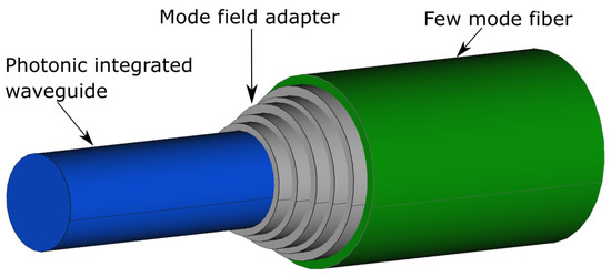
Figure 1.
Mode field adapter—spot size converter illustration.
We used an algorithm performing calculations in Python to design and obtain the interconnecting tapered structure among two dissimilar few-mode cores (Figure 2). Construction of the MFA consists of the design of specific structures for every desired mode to transmit. Afterwards, the resulting structures are compared in order to select the most suitable structure based on the resulting difference in MFDs for each mode and the best transmission efficiency. For simplicity, we based our analysis on waveguides of circular cross-section cores with a step index profile, although the same procedure can be followed for different core geometries, as discussed further in this text.
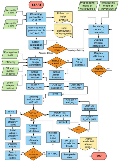
Figure 2.
Flowchart of the algorithm to obtain an MFA optimized for a specific mode between two different optical waveguides.
For circular-like cross-section waveguides, calculations to estimate the mode field adapters have been widely described by different reports [32]. Since, for different optical waveguides, the core can present different geometries, dimensions and various refractive index profiles or contrast, the typical way to define the MFD consists of analyzing the light distribution at the output of the waveguides [33]. However, for optical fibers, such as standard step index single-mode fibers, an approximation based on the linearly polarized (LP) modes can be defined by calculating the effective mode area (A) [34]:
where E represents the electric field amplitude distribution for the given LP mode under analysis, and the mode diameter is represented as 2w.
Thus, assuming circular core waveguides, we focus our analysis on the case where a waveguide from an integrated photonic device is interconnected to a few-mode fiber. The connecting structure is considered as an extension of the integrated waveguide, where both are made of a photosensitive polymer and fabricated with the DLW technique. Firstly, propagating modes are calculated in both waveguides under analysis, taking into account their materials, refractive index contrast, dimensions and signal wavelength. The propagation constants (), effective refractive index (), normalized frequency (V), MFDs and are determined as an outcome of these calculations. Then, for each specific LP mode, the MFDs from both waveguides are compared to establish the difference among them and set the parameters of the MFA. Depending on the difference between the two waveguides, the analysis span (), number of points to analyze (m) and the desired target efficiency are also defined. Using as a starting point the waveguide fabricated by the DLW technique, a new structure is defined, decreasing or increasing its diameter (depending on what is necessary), searching for the desired efficiency () and calculating the overlap integral (3), defined as:
where and are the electric field amplitude distributions of the waveguide and the fiber, respectively. Similarly, and are complex conjugates of the electric field amplitude distributions [24]. Then, the new diameter is set as the new DLW core waveguide and a new increment is calculated until the MFD of the DLW waveguide and the optical fiber are paired within the efficiency tolerance previously defined. This procedure is applied for each of the transmitted modes in both waveguides.
Based on these calculations, the interconnecting structure is computed, searching for the mode field area of the initial diameter and the entire profile. In this process, the waveguide from the PIC is taken as a starting point and the interconnecting structure is a continuation of this waveguide but with a diameter repeatedly modified. As a result, a set of values of different mode effective areas () is obtained, where the parameters of the optical fiber are kept as a target (). Every diameter variation is analyzed for a given span of different radii and calculating the corresponding coupling efficiency by means of the overlap integral. The adjusted radius that generates the desired efficiency is selected as a new point in the MFA profile. The process continues, adding points to the MFA profile until the MFD of the connecting waveguide and the optical fiber are paired ( = ) or the next increment is less than the efficiency difference set per step. In Figure 3, this is illustrated by showing the efficiencies resulting from the overlap integral while the core diameter varies in the m points within a defined span and how the selected diameters start to build the structure.
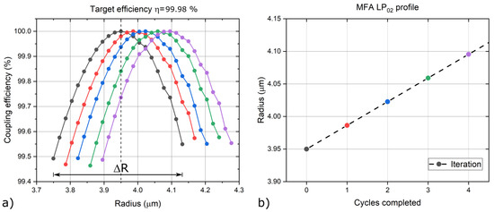
Figure 3.
Analysis of the diameter variation aiming to match the target waveguide. (a) Coupling efficiencies while varying the diameter within a defined span, taking as starting point different diameters (each color trace represents the possible coupling efficiencies for every iteration). (b) First points of mode field adapter profile designed for the mode.
The products of this algorithm are multiple MFA profiles based on the different propagating modes. Depending on the amount of modes to transmit from one side to another will be the number of possible structures to be defined with the proposed method. Nevertheless, this does not indicate the total length of the MFAs. To define the necessary length of the final MFA, an adiabaticity criterion must be included. A simple approach for an adiabatic structure is to consider that small variations in the core over a large distance, such as the light in the propagated mode, will not be transferred to a higher order mode; then, it is considered lossless. The main consideration to achieve this criterion is based on the beat length of the mode under analysis and the following higher mode [35]. Considering concentric cores and symmetrical modes, coupling occurs only among other symmetrical modes [36]. Normally, under this consideration, considerably large structures involve a core tapering angle small enough to avoid mode coupling [37,38]. Recent works have investigated other alternatives for deducing an optimized adiabatic length for a minimal footprint [39,40,41].
As an example case, we present a study of the interconnection between a PIC fabricated using the DLW technique and an FMF. We contemplate the interconnecting waveguide of the same material as the waveguides of the PIC and with the same fabrication method. We propose the fabrication of the structures using the low absorption DLW since this technique allows us to fabricate tridimensional structures. This technique can be applied in different photoresist using visible wavelength laser sources, although a wavelength of nm is the most commonly employed [30]. Additionally, structures generated by this technique can be further exposed to other light sources, discarding the developing procedure and embedding the structure in the rest of the polymeric material [42]. Alternatively, other polymeric materials can be used to cover the interconnecting structure. Thus, using polymeric materials with this technique serves as a packaging method as well.
Specifically, we base our calculations considering a negative photoresist (SU-8) for the PIC and MFA. For compatibility with the C-band telecommunication, the material has a refractive index of n = 1.5551 at nm [43]. We consider an MFA core generated by DLW and the rest of the photoresist cured under ordinary UV-LED exposure ( nm). Because of the double exposure, the refractive index contrast between the core and cladding is considered to be = 20 ×, which is in the range of the values generated in this process [44]. The example to discuss consists of the interconnection of an output waveguide of PIC of core radius m to a 4-LP FMF able to transmit the , , and modes with a refractive index of n = 1.444, × and m at the same wavelength [45].
Following the proposed methodology, four different interconnecting structures were designed and created considering the four modes. These MFAs designed for the , , and are called E1, E2, E3 and E4, respectively. As mentioned above, the length (L) of the structures was defined using the ordinary adiabaticity criterion. The resulting radial profiles of the four structures are plotted in Figure 4. Since the most common way to produce an interconnection between PICs and fibers consists of just using structures that match the dimensions of the two cores, this scenario is also included and used as a reference point. Therefore, linear and exponential structures only linking the starting and finishing diameters are also illustrated. The performance of the structure will be discussed in the following section.
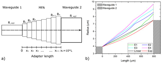
Figure 4.
(a) Scheme of iterative method of MFA design. (b) Mode field adapter profiles designed based on the different linearly polarized (LP) fiber modes: E1 for the , E2 for the , E3 for the and E4 for the . Additionally, linear and exponential profiles joining the two waveguide cores are included.
3. Results
The most favorable structure is selected from those obtained using the algorithm previously described to act as the MFA. Such a task requires the comparison of the MFDs achieved in all the structures. Further propagation simulations are required to determine the total efficiency and guiding conditions of the selected structure. The analysis of the MFAs designed for the example mentioned above and the validation of the results are discussed in the following sections.
3.1. Modal Distribution in MFAs
As an initial scenario, in Figure 5, we present the case where only the diameters of both cores are matched with a lineal tapered structure. In this scenario, even though the core diameters are equal at the interface, the effective refractive index will not be matched because of the different materials. Hence, the light distribution of every mode will be different in every section of the transmission link. As expected, the mode effective areas show a large mismatch between the two waveguide cores. This commonly used structure results in low efficiency and translates into high MDL.
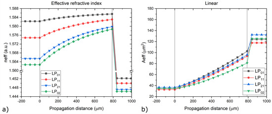
Figure 5.
Modal propagation conditions of an MFA with lineal profile matching only the diameters of the cores from the PIC to the FMF. (a) Effective refractive indices and (b) effective mode areas for the different LP fiber modes.
Based on the different MFAs previously designed, the examination of the modal propagation conditions is needed for determining the optimal MFA. A first approach is the calculation of the over the propagation length for all the propagated modes in each structure for further comparison. Figure 6 shows the obtained results for the designed structures considering the different propagated modes as well as the basic scenarios involving structures matching only core diameters (linear and exponential profiles). Since each mode involves a different , there is a noticeable difference in the final values for each mode in all the scenarios, thus presenting different spatial distributions.
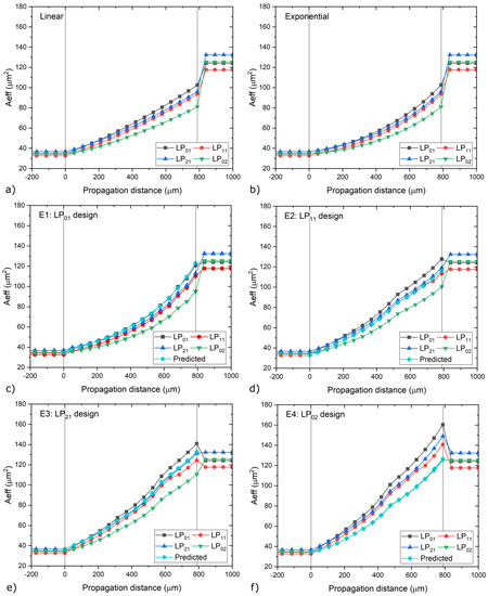
Figure 6.
Modal propagation conditions in the different MFA profiles: (a) linear, (b) exponential and optimized profiles for: (c) E1 for , (d) E2 for , (e) E3 for and (f) E4 for . Vertical lines indicate the boundaries of the PIC waveguide and FMF.
While designing a structure for the fundamental mode () results in a narrow structure, for the highest-order mode (), it yields a broader structure, as shown in Figure 4. The former case significantly crops the energy coupled into the FMF in higher-order modes, whereas the largest structure causes a considerable MFD increment for the lower-order modes compared to the ones of the FMF. Both cases represent a non-optimal structure for transmitting all the modes available in the photonic system to interconnect.
Analyzing the effective mode areas for the structures designed using the and modes, these present a more uniform distribution. For instance, the MFDs for the and modes of the interconnecting structure compared to the ones of the FMF are larger and smaller, respectively. Although there still exists a difference among all the values, the disparity is significantly reduced. Table 1 presents the absolute difference in effective mode areas between each MFA waveguide structure and few-mode fiber. Structure E2 presents the lowest difference among all the , where structure E3 has the lowest absolute values. Therefore, these two structures (E2 and E3) are better candidates for equalizing the transmission of all the modes and then further analysis is required to determine its efficiency.

Table 1.
Absolute difference in effective mode area at the interface between the interconnecting structure and the FMF.
3.2. Coupling Efficiency and Losses
To validate the performance of the selected structures, diverse simulations and calculations are performed. First, the mode mismatch is analyzed by means of the overlap integral using the resulting final diameter of the four calculated structures compared with the FMF and their respective mode effective areas. This calculation is performed for every LP mode and including as well the linear profile just pairing the diameters of the two cores (see Figure 7). As anticipated, the linear structure shows the worst performance, with the exception of the fundamental mode. It must be noticed that, for all the structures, the lower-order modes present a better pairing. The final diameter for the structure designed based on the mode reduces the differential mode matching among all the modes but the overall performance is the worst of all the designed structures. This can be attributed to the final diameter of the structure, which is the largest of all the structures. Structures E1, E2 and E3 present similar values while performing this calculation. Nonetheless, E1 also presents a larger differential mode matching. Hence, E2 and E3 are confirmed to be more suitable structures to be used as possible MFAs. Our calculations were performed using Equation (3) (solid line) with our algorithm using Python and corroborated with commercial software (Synopsys RSoft), presented as a dashed line.
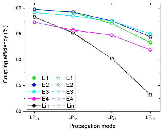
Figure 7.
Modal coupling efficiency for all possible interconnecting structures designed for specific LP modes, analyzing the MFDs at the boundary of the interconnecting structure and FMF by means of the overlap integral.
As structures E2 and E3 showed the best options for correct transmission for the given scenario, we performed additional simulations to evaluate their performance as MFAs. Light propagation was then evaluated using the beam propagation method (BPM) in the two structures using the BeamPROP package from RSoft, Synopsys. Since both structures present a non-conventional profile, a linear profile matching both core diameters was included for additional comparison (see linear, E2 and E3 profiles in Figure 4b). All structures are evaluated in terms of the adiabaticity length (L). The structure with the lineal profile (solid line) is first analyzed for three different lengths, as presented in Figure 8a, for further comparison with E2 (dotted line) and E3 (dashed line). It can be noticed that a length fulfilling the adiabaticity criterion slightly affects the modes, but making the structure longer reduce the losses and, thus, improves the efficiency. On the other hand, reducing, to some degree, the length of the MFA causes higher losses in a considerable manner. Additional losses are due to the refractive index difference between the PIC waveguide and FMF materials, resulting in 0.2 % intensity reflection.
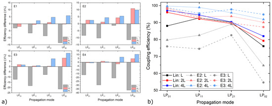
Figure 8.
(a) Coupling efficiencies for the structures E2 and E3 compared with a traditional linear profile for different transmission lengths. (b) Differential modal coupling efficiencies referenced a traditional linear profile for all the possible MFA structures.
Propagation of the studied four LP modes is then analyzed by means of BPM for the possible MFAs based on the profiles E1 to E4 with different lengths: and . Using as baseline the linear profile structure matching core diameters, the efficiency difference at the studied propagation lengths is presented in Figure 8a. For a short length, all structures present a performance reduction compared to the linear case, and the higher-order mode () is particularly penalized. When a longer propagation length is considered, major coupling efficiency is achieved. MFAs based on profiles E2 and E3 provide at least more efficiency for the mode (see Figure 8b). While E2 stands out for a considerable increase for all four modes, E3 records the maximum increment for the mode at a length of .
4. Discussion
The resulting structures following the proposed procedure present non-conventional profiles when compared to linear, exponential or sinusoidal structures. Upon comparing the performance for the fundamental mode, there is a slight benefit for using such structures. Nevertheless, when higher-order modes are transmitted, the benefit of using this method is more significant. This is of high relevance for recent systems employing slightly multimode signals in few-mode systems. By considering different possible structures, the transmission and efficiency features can be tuned and we can select the most convenient for the system. If a specific mode is intended to be transmitted, then this structure is designed taking into consideration this specific mode. Likewise, equalization of the transmitted modes when interconnecting PICs and FMFs can be achieved.
The most basic case consists of only matching the initial and final core sizes, and the transmission of light suffers higher penalties as the order of the mode increases (shown in Figure 7). In contrast, the creation of interconnects using our proposed algorithm allows one to obtain multiple possible structures for further analysis and comparison. Based on the results, one or more structures are selected for the optimum transmission of the different modes. By obtaining the absolute difference in mode effective areas, the structure yielding the least divergence grants a balanced power transmission along all the modes, thus minimizing the MDL.
In this work, we consider the use of the DLW technique, which yields integrated devices with directly compatible geometry and concentric with respect to the FMF. This scenario is a very attractive option while considering low contrast waveguides, allowing easy connection to optical fibers, such as those fabricated using dielectric materials. In addition, this approach allows us to easily fabricate the transition structures compared with other techniques since it is possible to use different materials, which can serve as intermediates for different platforms of PICs. Given the characteristics of the DLW technique, the non-conventional structures obtained by the algorithm can be achieved by either varying the power of the laser or the exposition time when scanning the material.
Although, in our simulations and calculations, we considered both the starting and ending waveguides of circular cross-sections, this is only a particular scenario. A more general scenario would be to consider an integrated photonic circuit fabricated using different types of waveguides, such as rectangular ones [24]. However, the proposed algorithm can be extended to other geometries and waveguide types (e.g., a waveguide with variable core geometry where the cross-section changes along the MFA).
Analysis adjustment of the waveguide will be required to calculate the mode effective area for the desired waveguide to study. This also applies for different refractive index profiles, requiring us only to modify the calculation of light distribution and propagation constants. Additionally, this method can be also applied for non-symmetrical cores such as elliptical or rectangular. In this case, two calculations, one for each axis, are required. For non-concentric waveguides, this algorithm could be modified to show coupling efficiency at the interface between two different materials and how this modifies the transmitted light for all modes. Considering this case, calculations can include misalignments in any direction in which the MFA can particularly couple light into specific modes. Nonetheless, the implications in the fabrication technique for a specific combination of parameters can be challenging.
Regarding the calculation of the optimal length for the structure, the calculation of optimized lengths is beyond the scope of this work. Nevertheless, the validation of the optimal transmission for the different modes is analyzed for different transition structures. A simple alternative is to use the standard guidelines for adiabatic tapered waveguides. The proposed algorithm can be complemented in combination with other methods focused on this specific subject [41,46]. We include basic analysis considering an ordinary adiabatic length for the MFA as well as in periodic increments, showing the advantages and disadvantages of the different interconnecting structures.
We only demonstrated a particular case where light transmission goes from the PIC to a FMF but it can be used to go either from the PIC to an optical fiber or the other way around. Alternatively, this algorithm can be applied not only to interconnect PICs to FMFs but to any optical waveguide and device. Nonetheless, ongoing research on this subject has been recently developed, trying to minimize the length of tapered spot size converters. Some reports utilize fast quasi-adiabatic dynamics, meta-materials or special topology structures, to mention a few examples [19,47,48]. It is worth mentioning that losses induced by reflections are minimal due to the low refractive index between the materials of the PIC and FMF. Considering other materials, such as silicon, the large refractive index difference among the materials will involve higher coupling losses given by reflections.
5. Conclusions
In this work, we propose an algorithm to assist the design of slightly multimode, or few-mode, interconnections between waveguides in integrated photonics and optical fibers. The proposed method allows the generation of a structure with better power transmission for all the available modes in the system. Our algorithm can design multiple structures to enhance the transmission of individual modes or a single structure to equalize the transmission of all the modes. The obtained structures demonstrate better performance than traditional structures with linear or exponential profiles. Therefore, this is a simple solution for the optimal coupling of higher-order modes in space and mode division multiplexing systems. The particular case of PIC and the mode field adapter made of a polymeric material is studied. Results from this analysis provided coupling efficiencies above 90 % for all the transmitted modes. Fabrication of tailored polymer-based interconnecting structures using the direct laser writing technique represents a cost-effective and uncomplicated option. The procedure presented in this work can be extended to different materials and configurations.
Author Contributions
Methodology, O.G.-C.; conceptualization, A.M.V.-B.; all authors contributed to the investigation, data analysis and manuscript writing. All authors have read and agreed to the published version of the manuscript.
Funding
This work was supported by UNAM-PAPIIT TA101220.
Institutional Review Board Statement
Not applicable.
Informed Consent Statement
Not applicable.
Data Availability Statement
The data that supports the findings of this study are available from the corresponding author upon reasonable request.
Acknowledgments
The authors wish to thank to Synopsys for the licensing of RSoft and CONACyT for the graduate program scholarship.
Conflicts of Interest
The authors declare no conflict of interest.
References
- Minzioni, P.; Lacava, C.; Tanabe, T.; Dong, J.; Hu, X.; Csaba, G.; Porod, W.; Singh, G.; Willner, A.E.; Almaiman, A.; et al. Roadmap on all-optical processing. J. Opt. 2019, 21, 063001. [Google Scholar] [CrossRef]
- Shi, W.; Tian, Y.; Gervais, A. Scaling capacity of fiber-optic transmission systems via silicon photonics. Nanophotonics 2020, 9, 4629–4663. [Google Scholar] [CrossRef]
- Ozawa, T.; Price, H.M.; Amo, A.; Goldman, N.; Hafezi, M.; Lu, L.; Rechtsman, M.C.; Schuster, D.; Simon, J.; Zilberberg, O.; et al. Topological photonics. Rev. Mod. Phys. 2019, 91, 015006. [Google Scholar] [CrossRef] [Green Version]
- Sinatkas, G.; Christopoulos, T.; Tsilipakos, O.; Kriezis, E.E. Electro-optic modulation in integrated photonics. J. Appl. Phys. 2021, 130, 010901. [Google Scholar] [CrossRef]
- Huang, L.; Xu, L.; Woolley, M.; Miroshnichenko, A.E. Trends in quantum nanophotonics. Adv. Quantum Technol. 2020, 3, 1900126. [Google Scholar] [CrossRef]
- Richardson, D.J.; Fini, J.M.; Nelson, L.E. Space-division multiplexing in optical fibres. Nat. Photonics 2013, 7, 354–362. [Google Scholar] [CrossRef] [Green Version]
- Leon-Saval, S.G.; Fontaine, N.K.; Salazar-Gil, J.R.; Ercan, B.; Ryf, R.; Bland-Hawthorn, J. Mode-selective photonic lanterns for space-division multiplexing. Opt. Express 2014, 22, 1036–1044. [Google Scholar] [CrossRef]
- Puttnam, B.J.; Rademacher, G.; Luís, R.S. Space-division multiplexing for optical fiber communications. Optica 2021, 8, 1186–1203. [Google Scholar] [CrossRef]
- Son, G.; Han, S.; Park, J.; Kwon, K.; Yu, K. High-efficiency broadband light coupling between optical fibers and photonic integrated circuits. Nanophotonics 2018, 7, 1845–1864. [Google Scholar] [CrossRef]
- Marchetti, R.; Lacava, C.; Carroll, L.; Gradkowski, K.; Minzioni, P. Coupling strategies for silicon photonics integrated chips. Photonics Res. 2019, 7, 201–239. [Google Scholar] [CrossRef]
- Hu, T.; Dong, B.; Luo, X.; Liow, T.Y.; Song, J.; Lee, C.; Lo, G.Q. Silicon photonic platforms for mid-infrared applications. Photonics Res. 2017, 5, 417–430. [Google Scholar] [CrossRef] [Green Version]
- Lin, H.; Luo, Z.; Gu, T.; Kimerling, L.C.; Wada, K.; Agarwal, A.; Hu, J. Mid-infrared integrated photonics on silicon: A perspective. Nanophotonics 2018, 7, 393–420. [Google Scholar] [CrossRef]
- Han, X.Y.; Wu, Z.L.; Yang, S.C.; Shen, F.F.; Liang, Y.X.; Wang, L.H.; Wang, J.Y.; Ren, J.; Jia, L.Y.; Zhang, H.; et al. Recent progress of imprinted polymer photonic waveguide devices and applications. Polymers 2018, 10, 603. [Google Scholar] [CrossRef] [Green Version]
- Maram, R.; Kaushal, S.; Azaña, J.; Chen, L.R. Recent trends and advances of silicon-based integrated microwave photonics. Photonics 2019, 6, 13. [Google Scholar] [CrossRef] [Green Version]
- Dietrich, P.I.; Blaicher, M.; Reuter, I.; Billah, M.; Hoose, T.; Hofmann, A.; Caer, C.; Dangel, R.; Offrein, B.; Troppenz, U.; et al. In situ 3D nanoprinting of free-form coupling elements for hybrid photonic integration. Nat. Photonics 2018, 12, 241–247. [Google Scholar] [CrossRef]
- Kohli, N.; Ménard, M.; Winnie, N.Y. Efficient TE/TM spot-size converter for broadband coupling to single mode fibers. OSA Contin. 2019, 2, 2428–2438. [Google Scholar] [CrossRef]
- Vanmol, K.; Baghdasaryan, T.; Vermeulen, N.; Saurav, K.; Watté, J.; Thienpont, H.; Van Erps, J. 3D direct laser writing of microstructured optical fiber tapers on single-mode fibers for mode-field conversion. Opt. Express 2020, 28, 36147–36158. [Google Scholar] [CrossRef]
- Gordillo, O.A.J.; Dave, U.D.; Lipson, M. One-to-one coupling higher order modes in a fiber to higher order modes in silicon waveguide. In Proceedings of the 2021 Conference on Lasers and Electro-Optics (CLEO), Virtual Event. 20–24 June 2021; pp. 1–2. [Google Scholar]
- Cheng, L.; Mao, S.; Chen, Z.; Wang, Y.; Zhao, C.; Fu, H. Ultra-compact dual-mode mode-size converter for silicon photonic few-mode fiber interfaces. Opt. Express 2021, 29, 33728–33740. [Google Scholar] [CrossRef]
- Sillard, P.; Bigot-Astruc, M.; Molin, D. Few-mode fibers for mode-division-multiplexed systems. J. Light. Technol. 2014, 32, 2824–2829. [Google Scholar] [CrossRef]
- Kumar, A.; Nambiar, S.; Kallega, R.; Ranganath, P.; Ea, P.; Selvaraja, S.K. High-efficiency vertical fibre-to-polymer waveguide coupling scheme for scalable polymer photonic circuits. Opt. Express 2021, 29, 9699–9710. [Google Scholar] [CrossRef]
- Park, S.R.; O, B.H. Novel design concept of waveguide mode adapter for low-loss mode conversion. IEEE Photonics Technol. Lett. 2001, 13, 675–677. [Google Scholar] [CrossRef]
- Mu, X.; Wu, S.; Cheng, L.; Fu, H. Edge couplers in silicon photonic integrated circuits: A review. Appl. Sci. 2020, 10, 1538. [Google Scholar] [CrossRef] [Green Version]
- Hardy, I.; Grosso, P.; Bosc, D. Design and fabrication of mode size adapter in a photosensitive polymer waveguide. IEEE Photonics Technol. Lett. 2005, 17, 1028–1030. [Google Scholar] [CrossRef]
- Qi, W.; Yu, Y.; Zhang, X. On-chip arbitrary-mode spot size conversion. Nanophotonics 2020, 9, 4365–4372. [Google Scholar] [CrossRef]
- Baldacchini, T. Three-Dimensional Microfabrication Using Two-Photon Polymerization: Fundamentals, Technology, and Applications; William Andrew: Norwich, NY, USA, 2015. [Google Scholar]
- Choudhury, D.; Macdonald, J.R.; Kar, A.K. Ultrafast laser inscription: Perspectives on future integrated applications. Laser Photonics Rev. 2014, 8, 827–846. [Google Scholar] [CrossRef] [Green Version]
- Chen, F.; de Aldana, J.V. Optical waveguides in crystalline dielectric materials produced by femtosecond-laser micromachining. Laser Photonics Rev. 2014, 8, 251–275. [Google Scholar] [CrossRef]
- Wu, Z.L.; Qi, Y.N.; Yin, X.J.; Yang, X.; Chen, C.M.; Yu, J.Y.; Yu, J.C.; Lin, Y.M.; Hui, F.; Liu, P.L.; et al. Polymer-based device fabrication and applications using direct laser writing technology. Polymers 2019, 11, 553. [Google Scholar] [CrossRef] [Green Version]
- Do, M.T.; Nguyen, T.T.N.; Li, Q.; Benisty, H.; Ledoux-Rak, I.; Lai, N.D. Submicrometer 3D structures fabrication enabled by one-photon absorption direct laser writing. Opt. Express 2013, 21, 20964–20973. [Google Scholar] [CrossRef]
- Lindenmann, N.; Balthasar, G.; Hillerkuss, D.; Schmogrow, R.; Jordan, M.; Leuthold, J.; Freude, W.; Koos, C. Photonic wire bonding: A novel concept for chip-scale interconnects. Opt. Express 2012, 20, 17667–17677. [Google Scholar] [CrossRef] [Green Version]
- Matsui, T.; Nakajima, K.; Sakamoto, T. Effective mode-field diameter for few-mode fibers for considering splice loss characteristics. Appl. Opt. 2017, 56, 7484–7490. [Google Scholar] [CrossRef]
- Nakamura, A.; Iida, D. Mode field diameter definitions for few-mode fibers based on spot size of higher-order Gaussian mode. IEEE Photonics J. 2020, 12, 1–9. [Google Scholar] [CrossRef]
- Nakamura, A.; Okamoto, K.; Koshikiya, Y.; Manabe, T. Effective mode field diameter for LP 11 mode and its measurement technique. IEEE Photonics Technol. Lett. 2016, 28, 2553–2556. [Google Scholar] [CrossRef]
- Love, J.; Henry, W.; Stewart, W.; Black, R.; Lacroix, S.; Gonthier, F. Tapered single-mode fibres and devices. Part 1: Adiabaticity criteria. IEE Proc. J. (Optoelectron.) 1991, 138, 343–354. [Google Scholar] [CrossRef]
- Black, R.; Lacroix, S.; Gonthier, F.; Love, J. Tapered single-mode fibres and devices. II. Experimental and theoretical quantification. IEE Proc. J. (Optoelectron.) 1991, 138, 355–364. [Google Scholar] [CrossRef]
- Sun, X.; Liu, H.C.; Yariv, A. Adiabaticity criterion and the shortest adiabatic mode transformer in a coupled-waveguide system. Opt. Lett. 2009, 34, 280–282. [Google Scholar] [CrossRef] [Green Version]
- Zou, J.; Yu, Y.; Ye, M.; Liu, L.; Deng, S.; Xu, X.; Zhang, X. Short and efficient mode-size converter designed by segmented-stepwise method. Opt. Lett. 2014, 39, 6273–6276. [Google Scholar] [CrossRef]
- Martínez-Garaot, S.; Ruschhaupt, A.; Gillet, J.; Busch, T.; Muga, J.G. Fast quasiadiabatic dynamics. Phys. Rev. A 2015, 92, 043406. [Google Scholar] [CrossRef] [Green Version]
- Martínez-Garaot, S.; Muga, J.G.; Tseng, S.Y. Shortcuts to adiabaticity in optical waveguides using fast quasiadiabatic dynamics. Opt. Express 2017, 25, 159–167. [Google Scholar] [CrossRef] [Green Version]
- Liang, T.L.; Tu, Y.; Chen, X.; Huang, Y.; Bai, Q.; Zhao, Y.; Zhang, J.; Yuan, Y.; Li, J.; Yi, F.; et al. A Fully Numerical Method for Designing Efficient Adiabatic Mode Evolution Structures (Adiabatic Taper, Coupler, Splitter, Mode Converter) Applicable to Complex Geometries. J. Light. Technol. 2021, 39, 5531–5547. [Google Scholar] [CrossRef]
- Sullivan, A.C.; Grabowski, M.W.; McLeod, R.R. Three-dimensional direct-write lithography into photopolymer. Appl. Opt. 2007, 46, 295–301. [Google Scholar] [CrossRef]
- Kayaku Advanced Materials. Permanent Negative Epoxy Photoresist Technical Data Sheet; Kayaku Advanced Materials: Westborough, MA, USA, 2020; Version 1. [Google Scholar]
- Glugla, D.J.; Chosy, M.B.; Alim, M.D.; Childress, K.K.; Sullivan, A.C.; McLeod, R.R. Multiple patterning of holographic photopolymers for increased refractive index contrast. Opt. Lett. 2018, 43, 1866–1869. [Google Scholar] [CrossRef] [PubMed]
- Sillard, P.; Bigot-Astruc, M.; Boivin, D.; Maerten, H.; Provost, L. Few-mode fiber for uncoupled mode-division multiplexing transmissions. In Proceedings of the 2011 37th European Conference and Exhibition on Optical Communication, Geneva, Switzerland, 18–22 September 2011; pp. 1–3. [Google Scholar]
- Siriani, D.F.; Tambasco, J.L. Adiabatic guided wave optics—A toolbox of generalized design and optimization methods. Opt. Express 2021, 29, 3243–3257. [Google Scholar] [CrossRef] [PubMed]
- Wu, Y.L.; Liang, F.C.; Chung, H.C.; Tseng, S.Y. Adiabaticity engineering in optical waveguides. Opt. Express 2020, 28, 30117–30129. [Google Scholar] [CrossRef] [PubMed]
- Sun, L.; Zhang, R. Metamaterial-based ultrashort multimode waveguide taper with low intermodal crosstalk. Opt. Express 2021, 29, 7124–7133. [Google Scholar] [CrossRef]
Publisher’s Note: MDPI stays neutral with regard to jurisdictional claims in published maps and institutional affiliations. |
© 2022 by the authors. Licensee MDPI, Basel, Switzerland. This article is an open access article distributed under the terms and conditions of the Creative Commons Attribution (CC BY) license (https://creativecommons.org/licenses/by/4.0/).