Communication

On the Selective Spectral Sensitivity of Oppositely Placed Double-Barrier Structures

1
Optoelectronic Devices Laboratory, National Polytechnic University of Armenia, Yerevan 0009, Armenia
2
International Clean Water Institute, P.O. Box 258, Manassas, VA 20108, USA
3
Institute of Electronic Engineering and Nanotechnologies “D. Ghitu”, Academy of Sciences of Moldova, MD-2004 Chisinau, Moldova
4
Faculty of Civil Engineering, Transylvania University of Brasov, 500152 Brasov, Romania
*
Author to whom correspondence should be addressed.
Photonics 2022, 9(8), 558; https://doi.org/10.3390/photonics9080558
Submission received: 3 July 2022 / Revised: 2 August 2022 / Accepted: 4 August 2022 / Published: 9 August 2022

Abstract

:
The characteristics of an oppositely placed double potential barrier photodetector structure were investigated under longitudinal illumination. The functional abilities of the silicon n+-p-n+ structure were studied under longitudinal illumination. The choice of impurity concentration in the n+- and p- regions provided the difference in heights of the potential barriers near-surface, rear, and oppositely directed regions and their conjoining in the high-resistance p-base. The widths of the depletion regions of these barriers varied with a step change in the bias voltage. The redistribution of the fraction of absorption of electromagnetic waves between the barriers and the change in their contribution to the total photocurrent was investigated. In connection with this, short-wavelength (490 nm) and long-wavelength (830 nm) spectral maxima were formed. In the voltage range commensurate with the difference in the heights of the potential barriers, the inversion of the sign of the spectral photocurrent and, using the developed algorithm, the spectral distribution of the absorbed radiation intensity, were obtained. A physical explanation of these results is provided. The structure under investigation enables the selective registration of individual waves and their intensities. The results reported here enable an optimistic spectrophotometric outlook for oppositely placed double-barrier photonic structures.

1. Introduction

The operation of an optical monitoring system is grounded in its quantitative and qualitative assessment of the composition of optically transparent materials, based on the output optical response [1,2]. A wide range of applications is anticipated in agriculture, veterinary investigations, food and beverage industries, fermentation industry, wastewater management, environment defense against pollutants and radiations, clinical diagnosis, drugs monitoring, mining, polymer production, and many other similar fields. Due to their widespread use, further improvements in such optical systems should be aimed at their miniaturization, low-cost production, high accuracy, and high sensitivity, especially for real-time remote monitoring of harmful substances [3,4,5]. Modern monitoring systems are expensive and do not, as yet, have miniaturized dimensions for portability. Such systems consist of optical diffraction grids, light filters, prisms, and high-accuracy mechanical rotation nodes [1,2]. As a result, the use of these systems in non-laboratory conditions, especially in field applications, becomes problematic. The best solution for such issues is by the usage of spectrum sensitive and miniature semiconductor photodetectors in monitoring systems, instead of complex and expensive mechanical–optical nodes.
Currently, research is actively conducted by the international scientific community in progressing the development of semiconductor photodetectors for monitoring systems based on traditional (silicon, germanium, A3B5), as well as thin-film and 2D (graphene, perovskite, silicon carbide) semiconductors [6,7,8,9,10,11,12]. Special schematic and design-technological solutions are used to ensure the spectral selectivity of these photodetectors [13,14,15,16,17,18,19,20]. They have multilayer structures or a number of active cascade layers with different substrate thicknesses. According to the depth of penetration of individual waves, different degrees of photoconductivity are obtained. The spectral intensity distribution is obtained by mathematical processing of the measurement results. However, high-precision registration by these structures requires identical absorption conditions and the creation of nano-precise multilayer structures. Complex fabrication technology and a lack of ability to control the spectral sensitivity by an external voltage render it difficult to fabricate and use in such structures.
In this study, we investigated a new approach and, on its basis, a photodetector structure in which, by using the structure of an oppositely placed double potential barrier (DPB), we could record the spectral composition of the integral radiation emerging from the optically transparent medium under study, in the wavelength range of 350–1000 nm. Using the algorithm developed for this investigation, the proposed structure allowed for spatial separation of information embedded in waves with greater accuracy than in [21,22,23], under conditions of longitudinal absorption of electromagnetic radiation; the algorithm was also used to obtain the spectral distribution of the intensity of these waves. Thus, the spectral composition of the photo signal coming from the test substance was selectively recorded. This paper presents the results of our comprehensive study of the characteristics of DPB photodetectors.

2. Structure and Experiment

Figure 1 shows a cross-section of the DPB photodetector silicon structure. The high-resistivity base region of the investigated structure with p-type conductivity was located between the low-resistivity 𝑛+ regions and had a thickness of 5.5 μm. It was covered by the space charges region on both sides, which could be regarded as thin n–p junctions since they were much narrower than the diffusion length of electrons and holes. In this regard, the charge carriers passed through the space-charge layer without recombination, i.e., we could assume that there was no recombination in the regions of the n–p junctions. Thus, in the samples under investigation, the recombination currents did not have a significant influence on the total photocurrent. This was also true for the radiation absorption of the impurities (they were all ionized at room temperature), on the free carriers, excitons, and tunneled carriers through the barriers. All the above-mentioned mechanisms contributed to the contributions in the long-wave region of the spectrum only at low temperatures [24].
The samples were fabricated using the technological capabilities of the RD Alfa Microelectronics Laboratory (Riga, Latvia). On an n-type silicon substrate having (100) orientation, with a resistivity of 0.01 Ω cm, and a thickness of 460 nm, a base with a thickness of ~5.5 μm was epitaxially grown, with a cathode depth at 0.3 μm. The effective film thickness was ~5.8 µm. The impurity concentration in the base was 1.2 × 1014 cm−3, the impurity concentration in the cathode was 5 × 1018 cm−3, and in the substrate was 1 × 1018 cm−3. Thus, it was possible to cover the base with depleted areas of oppositely directed potential barriers (DPB).
The DPB photodetector samples were irradiated with several sources of light with different spectral peaks. The total radiation and the individual light sources with wavelength λ = 300–1000 nm measured through the monochromator, were used for this research investigation. To obtain the I–V characteristics and spectral characteristics, a Keithley 6340 Sub-Femtoamp RemoteSource Meter Instrument (Cleveland, OH, USA) was used to apply stepwise voltage to the photodetector, with a step of 1 mV. The 6½-digit Model 6430 Sub-Femtoamp RemoteSource Meter Instrument could measure current with 1 nA sensitivity.

3. Results and Discussion

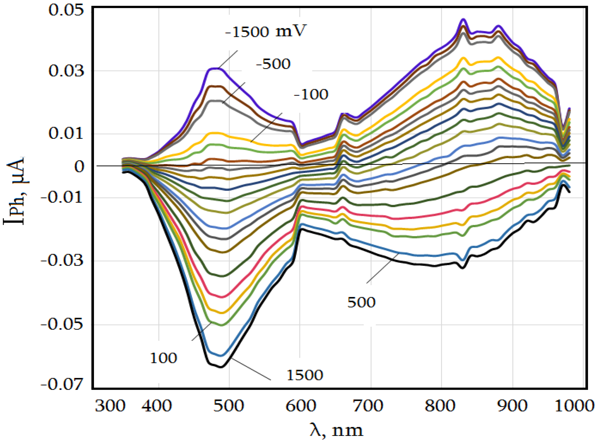
Spectral dependence of the photocurrent (IPh) of DPB photodetector samples at different bias voltages (in mV) is shown in Figure 2.
The spectral response had the following features:
  • When the voltages were positive, the near-surface barrier was reverse-biased and the rear barrier was forward-biased. When the polarity changed, the opposite effect was observed. Since the near-surface barrier was 0.04 eV higher than the rear barrier (see Figure 1), the photocurrent was determined by the near-surface barrier and remained negative within the wavelength range of 350–600 nm when the bias voltage changed from positive to negative up to −0.04 V;
  • With the increase in the wavelength, the influence of the reverse photocurrent of the rear barrier gradually increased, and the total photocurrent passing through the short-wave maximum (in the wavelength region of 490 nm) dropped, since, due to the exponential absorption law, the quanta fell deeper and the generated photocurrent of the rear junction began to counteract the photocurrent of the near-surface barrier;
  • At a wavelength of 600 nm, the rear photocurrent became commensurable with the surface photocurrent. The maximum compensation of the opposed photocurrents occurred, which was determined by the minimum value of the absolute photocurrent. Within the wavelength range of 600–1000 nm, with an increase in the wavelength, the photocurrent that was mainly determined by the rear barrier increased in the absolute value and, in the region of the intrinsic absorption of silicon, formed a long-wave maximum, which, at high negative voltages, was in the wavelength region of 830 nm. With the decrease in the voltage in the absolute value, the maximum shifted towards the long waves and reached the wavelength region of 880 nm. Here, a certain role was assumed by the rear out-of-the-base region, which was wide enough to ensure the diffusion current of the rear junction and the effective absorption of the deeply penetrated long waves;
  • At the positive biases, the near-surface barrier was reverse-biased, and with the decrease in the voltage, the long-wave maximum (830 nm) shifted towards the short waves (730 nm) since the height of the near-surface barrier decreased, and the influence of its photocurrent preserved the advantage only when the waves were shorter (i.e., with the decrease in the absorption depth).
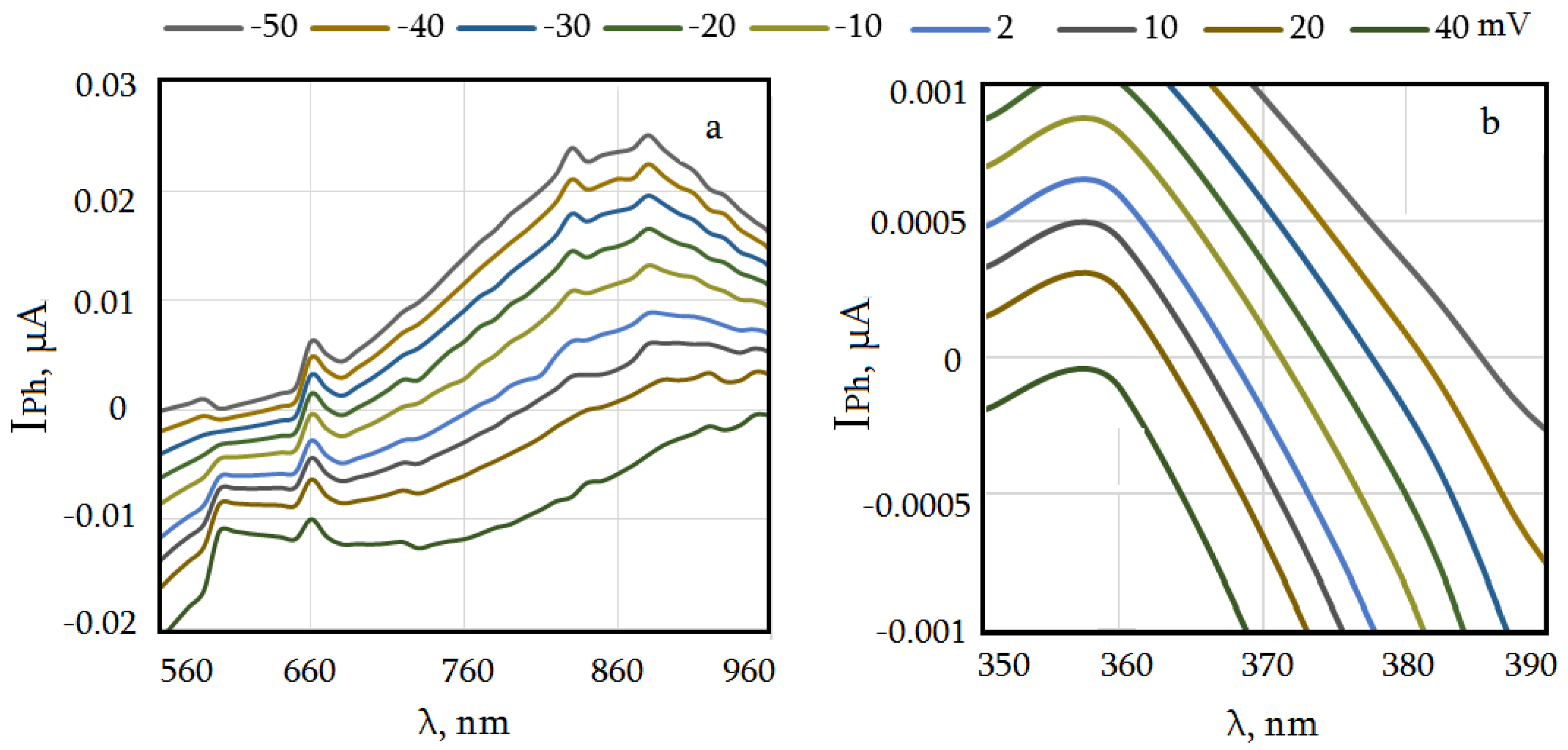
Another feature of Figure 2 is the presence of the change of the spectral photocurrent sign within the bias voltage range of −0.050–+0.040 V. Outside this range, the sign change did not occur because of the domination of the photocurrent of the reverse-biased near-surface or rear barriers. Within the mentioned voltage range, the short-wave photocurrent of the near-surface barrier and the long-wave photocurrent of the rear barrier had the advantage. Figure 3 presents a detailed description of the change in the spectral photocurrent sign in the long-wave (Figure 3a) and short-wave (Figure 3b) regions of the spectrum.
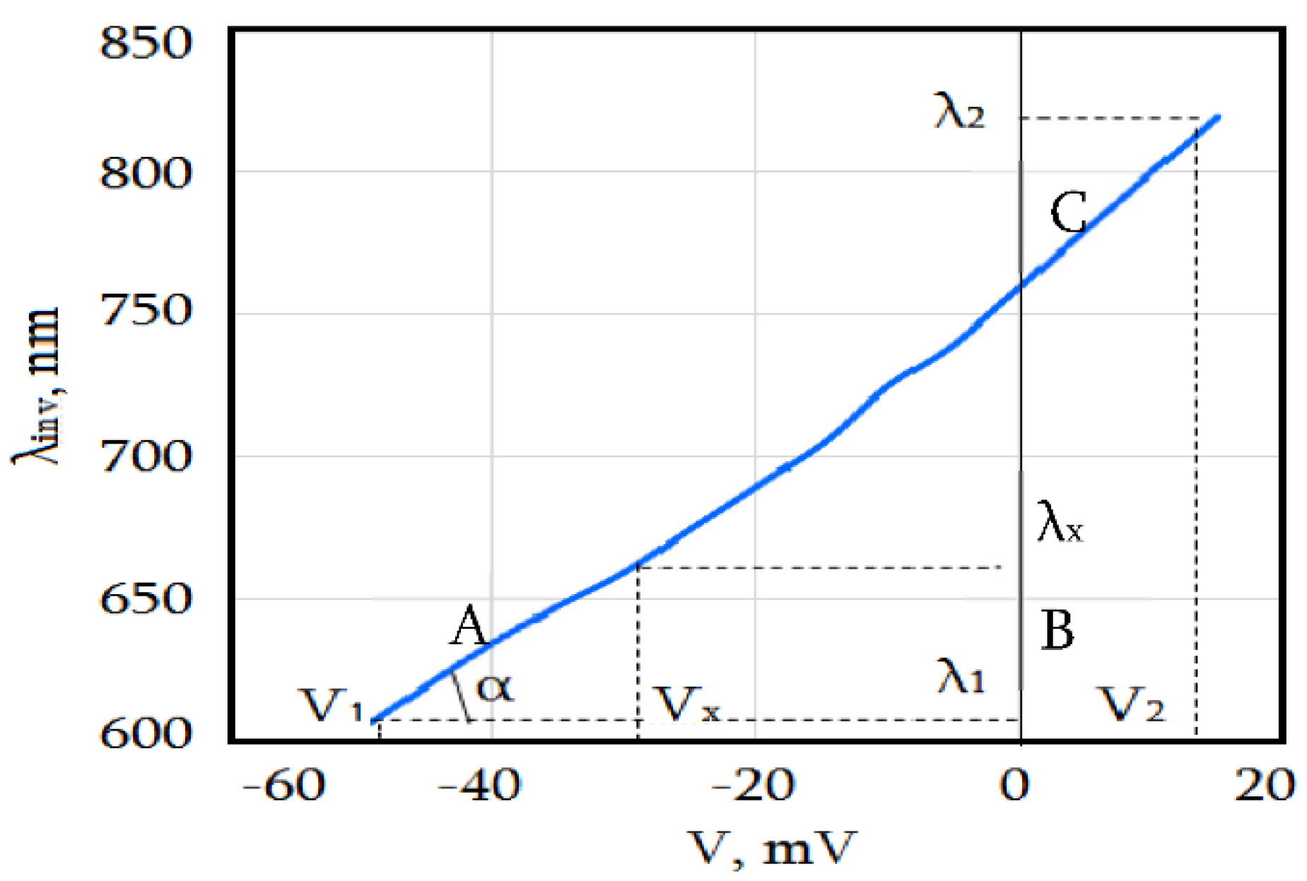
Within the stated voltage range, when moving from the positive voltage to the negative voltage, the height of the near-surface barrier decreased, and at −0.04 V became commensurable with the height of the rear barrier. The studies show that within the wavelength range of approximately 550–850 nm, the dependence of the inversion point of the spectral photocurrent on the bias voltage λinv = f(V) has a linear character (Figure 4. The unknown wavelength is determined by the slope of such inversion point dependence, by the equation,
λ x = V x ( λ 2 λ 1 ) + λ 1 V 2 λ 2 V 1 V 2 V 1
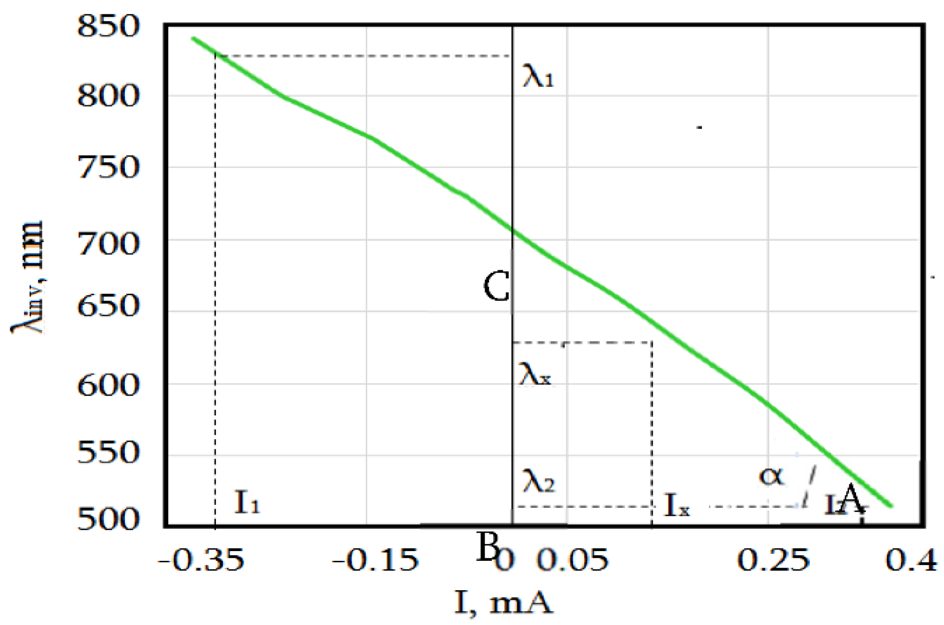
Within the stated voltage range, the dependence of the inversion point of the spectral photocurrent on the photocurrent (λinv = f(I)), which is obtained by the integral flux of the radiation containing wavelengths of 550–850 nm, also has a linear character (Figure 5). The same feature is preserved in the short-wave region of the spectrum within the wavelength range of 350–380 nm (Figure 6).
It is obvious that, within the voltage range at which the change in the spectral photocurrent sign occurs, the unknown wavelength in the absorbed integral radiation can also be determined by the value of t g α from the linear dependence (λinv = f(I)) of the inversion point of the spectral photocurrent on the total photocurrent, from the triangle ABC in Figure 4, by the following equation,
λ x = I x ( λ 2 λ 1 ) + λ 1 I 2   λ 2 I 1 I 2 I 1
Thus, in the presence of the difference in the heights of the oppositely directed joined potential barriers, the photocurrent flowing through the structure changes its sign at the voltages corresponding to that difference. The logic of the algorithm for the selective sensitivity is the following: when the bias voltage is changed, the widths of the depleted regions of the barriers change—one at the expense of the other— and the relation of the absorption fraction of the quanta of the penetrated wave changes in both barriers. It leads to the change in the total photocurrent, which is mainly conditioned by the wave that has the predominant intensity in the integral flux of the absorbed radiation at that depth. Under these conditions, the difference in the photocurrents corresponding to the nearest values of the voltage applied to the photodetector may mostly be determined by one wave. Thus, it is possible to calculate the wavelength and its intensity by a step-by-step change in the bias voltage with the help of the previously obtained mathematical model.
The mathematical modeling of the photoelectronic processes, which is used in the algorithm of the spectral distribution of the radiation intensity, contains an expression for the determination of the position of the junction point of the depleted regions of the structure, which is obtained by solving the Poisson equation [23]:
x m = d x 0 2 ε ε 0 ( Δ φ qV ) N d q 2 ( d x 0 ) ,
where N d is the p-type impurity density in the base, ε is the relative permittivity of the substance, ε 0 is the permittivity of the free space, q is the electron charge, V is the bias voltage, x 0 is the thickness of the near-surface layer, d is the base width, Δ φ = φ b 1 φ b 2 is the difference in the heights of the potential barriers.
In Equation (1), x m changes linearly from x 0 up to d with the change in the bias voltage. It means that the absorbed quanta are uniformly redistributed between the depleted regions within the range of the bias voltage change according to the exponential law.
Under the conditions of the irradiation with the integral flux, the expression for the photocurrent can be presented as shown in [23],
i , j I Ph   ij = qS i F i 0 ( 1 2 e α i x mj + e α i d 1 + α i w ) ,
where i = 1 ,   2 ,   3 changes with the change in the radiation wavelength in the integral flux, j = 1 ,   2 ,   3 changes with the change in the bias voltage, F ( λ i ) is the total flux of the incident photons with the wavelength of λ i , α i is the absorption coefficient of the electromagnetic radiation, S is the photosensitive area, w is width of the rear n-region, F 0 = P opt ( 1 R ) / Sh ν is the total flux of the incident photons per unit area, P opt is the radiation power, R is the reflection coefficient, h is Planck’s constant, ν is the frequency of the electromagnetic radiation, and q is the electron charge.
In Equation (2), the width of the rear n-region, w, is less than the diffusion length of the holes L p , and the value of L p is replaced by w (see Figure 1). From Equation (2), we receive the photocurrent of an individual wave and its intensity.
I = qSF 0 ( 1 2 e α i x mj + e α i d ) ,   F 0 = I / qS ( 1 2 e α i x mj + e α i d 1 + α i w ) .
With the sufficient value of x m , the fraction of the penetrated short waves decreases and, with the step-by-step change (small steps) in the external voltage, the redistribution of the absorbed quanta of each wave takes place. The major contribution to the photocurrent change is made by the wave that has the highest intensity at depth x m , and that wave will be registered. Thus, the step-by-step registration of individual waves and their intensities is carried out.
The experimentally obtained photocurrents are so small that they can be transformed by means of the Maclaurin series around the point x m . As a result, an expression for the absorption coefficient is obtained as,
α = 2 A ( x m 2 x m 3 ) x m 1 + x m 2 A ( x m 2 2 x m 3 2 ) x m 1 2 + x m 2 2 ,
where A = ( I 1 I 2 ) / ( I 2 I 3 ) is determined from the Volt–ampere characteristics (CVC) of the neighboring values of the photocurrents that correspond to the values of x m 1 ,   x m 2 ,   x m 3 .
Next, the numerical values of the absorption coefficient and the corresponding wavelengths of the electromagnetic radiation in silicon [23], obtained by the transition from α to λ with the help of the special program, are used. This makes it possible to obtain the spectral distribution of the absorbed radiation intensity in the Excel environment in automatic mode.
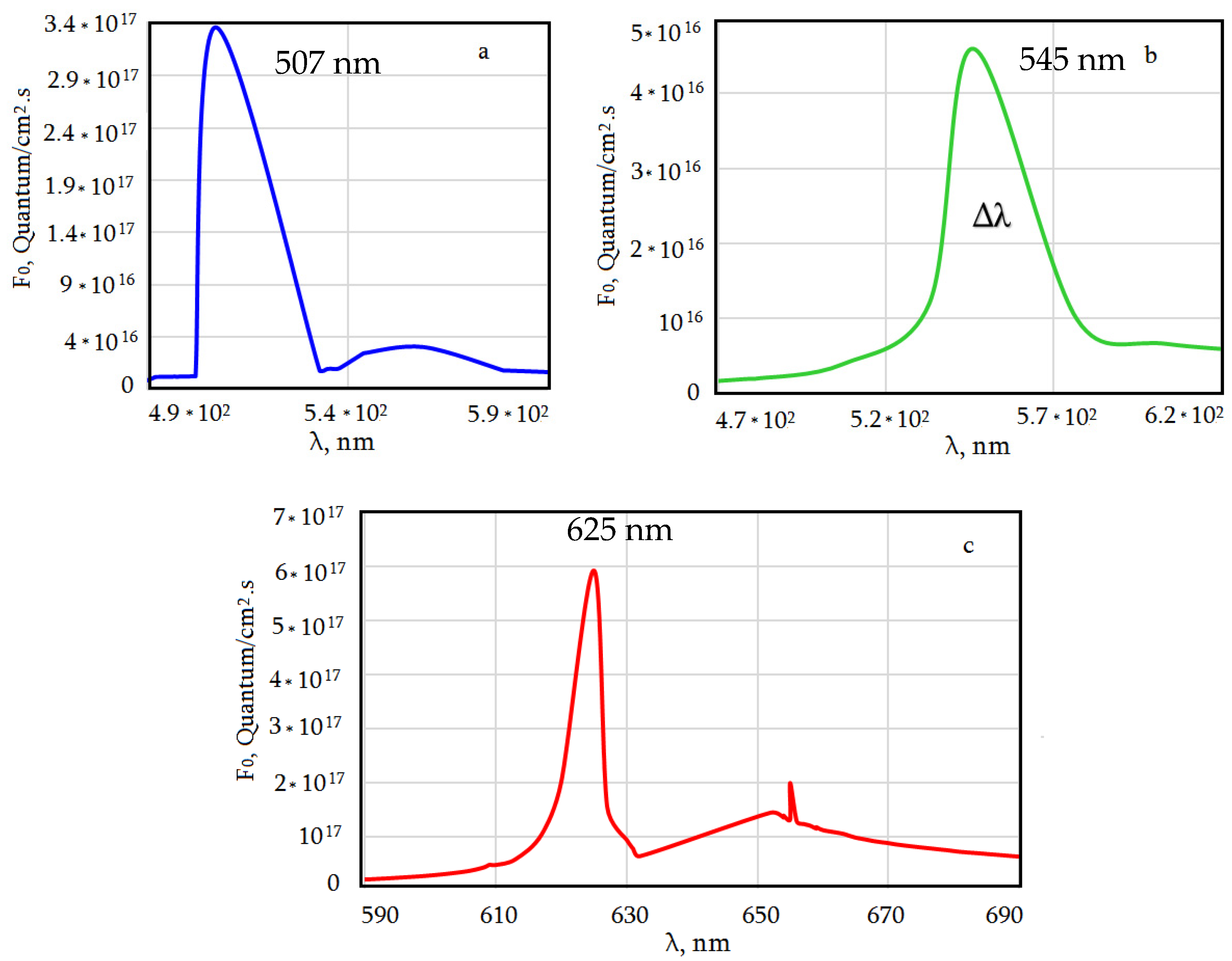
The powers of individual waves used in the experiment, upon the recalculation of the intensity, are presented in Figure 7a. The integral photocurrent when absorbing these waves was directed towards the input of the corresponding algorithm by the step-by-step change in the bias voltage with the step of 1 mV, and the experimental spectral distribution of the intensity was obtained at its output (Figure 7b). Using this algorithm, the emission distribution spectra of blue LL-304BC4B-B4-1GD (AlGaInP), green L53GC (GaP), and red KBT KP-2012EC (GaAsP/GaP) LEDs were obtained. The spectral peaks of the LEDs were at 470 nm, 565 nm and 625 nm, respectively. The spectral peaks we obtained were 507 nm, 547 nm, and 625 nm, respectively. Thus, there was a discrepancy for blue 37 nm and green 18 nm. For red, there was no discrepancy. Previously, we obtained very narrow spectral peaks [22,23]. In the present work, spectral distributions with a half-width ∆λ (shown in Figure 8 for green radiation) were obtained, which were closer to the reference distributions of the spectral intensity of LEDs (Figure 8). Thus, when using this algorithm, a more accurate distribution of the spectra of LEDs was obtained. In further work, by changing the design and technological parameters and nuances in the algorithm, we will strive to achieve even higher spectral accuracy.

4. Conclusions

As a result of the work carried out, under longitudinal illumination, a silicon structure with two oppositely directed potential barriers was studied. Their depleted areas had a docking point, which allowed, with a change in the bias voltage, to change the widths of one of the depleted regions at the expense of the other. As a result, the proportion of absorption of electromagnetic waves was redistributed between the barriers, and mutual compensation of oppositely directed photocurrents occurred. In the region of short wavelengths, the photocurrent of the near-surface barrier had an advantage, and in the region of relatively long wavelengths, while the photocurrent of the rear barrier had an advantage. As a result, short-wavelength (in the region of λ = 490 nm) and long-wavelength (in the region of λ = 830 nm) spectral maxima of the photocurrent were formed.
In the voltage range (commensurate with the difference in the heights of potential barriers equal to ~0.04 eV) that increased the height of the lower (reversely biased) barrier until it compared with the height of the high barrier, an inversion of the sign of the spectral photocurrent was obtained, in the wavelength range of 355 nm to 385 nm in the short-wavelength part of the spectrum, and from 600 nm to 830 nm in the long-wavelength part of the spectrum. Outside this range, the sign did not change and was determined by the sign of the applied voltage. The sign change point of the spectral photocurrent depended linearly on the bias voltage. This resulted in a linear change in the location of the depleted regions’ docking point, with the bias voltage. As a result, there was a uniform redistribution of the absorbed quanta between the depleted regions, when the bias voltage changed. With a step change in the voltage (with a small step of 1 mV), in this voltage range, it became possible to isolate individual waves and their intensities and obtain a spectral distribution of intensities. In this case, the spectral accuracy increased, and the mismatch of the peaks decreased, moving from blue (37 nm) to red (0 nm). In further work, by changing the design and technological parameters and nuances in the algorithm, we will strive to achieve even higher spectral accuracy.

Author Contributions

Conceptualization, S.K. and G.A.; methodology, L.M. and A.K.; software, A.K. and M.K.; validation, S.K., G.A., A.V. and L.M.; formal analysis, S.K.; investigation, S.K. and G.A.; resources, S.K.; G.A.; data curation, A.K.; writing—original draft preparation, S.K.; writing—review and editing, S.K. and A.V.; visualization, M.K. and E.M.; supervision, S.K. and G.A.; project administration, S.K.; funding acquisition, S.K. All authors have read and agreed to the published version of the manuscript.

Funding

The work was supported by the Science Committee of the Republic of Armenia in the frames of the research projects No. 21AG-2B011 and No. 21T-2B028.

Institutional Review Board Statement

The authors declare that no human and/or animal subjects were involved, and no cell lines were used for this investigation.

Informed Consent Statement

Not applicable.

Data Availability Statement

The datasets generated and/or analyzed during the current investigation are available from the corresponding author upon reasonable request.

Conflicts of Interest

The authors declare no conflict of interest, financial or otherwise.

References

  1. Worsfold, P.; Zagatto, E. Spectrophotometry-Overview. In Encyclopedia of Analytical Science, 3rd ed.; Worsfold, P., Poole, C., Townshend, A., Miró, M., Eds.; Academic Press: Oxford, UK, 2019; pp. 244–248. [Google Scholar]
  2. Thomas, O.; Burgees, C. UV-Visible Spectrophotometry of Water and Wastewater, 2nd ed.; Elsevier Science: London, UK, 2017; p. 2. [Google Scholar]
  3. Global Spectrophotometer Market 2020–2024. Available online: https://www.researchandmarkets.com/reports/5157122/global-spectrophotometer-market-2020-2024 (accessed on 24 June 2022).
  4. Albert, D.R.; Todt, M.A.; Davis, H.F. A Low-Cost Quantitative Absorption Spectrophotometer. J. Chem. Educ. 2012, 89, 1432–1435. [Google Scholar] [CrossRef]
  5. Bui, D.A.; Hauser, P.C. Analytical Devices based on Light-emitting Diodes-a Review of the State-of-the-Art. Anal. Chim. Acta 2015, 853, 46–58. [Google Scholar] [CrossRef] [PubMed]
  6. Fang, Y.; Armin, A.; Meredith, P.; Huang, J. Accurate Characterization of Next-Generation Thin-Film Photodetectors. Nat. Photonics 2019, 13, 1–4. [Google Scholar] [CrossRef]
  7. Zhang, T.; Wang, F.; Zhang, P.; Wang, Y.; Chen, H.; Li, J.; Wu, J.; Chen, L.; Chen, Z.D.; Li, S. Low-temperature Processed Inorganic Perovskites for Flexible Detectors with a Broadband Photoresponse. Nanoscale 2019, 11, 2871–2877. [Google Scholar] [CrossRef] [PubMed]
  8. Xu, Y.; Lin, Q. Photodetectors Based on Solution-processable Semiconductors: Recent Advances and Perspectives. Appl. Phys. Rev. 2020, 7, 011315. [Google Scholar] [CrossRef]
  9. Huo, N.; Konstantatos, G. Recent Progress and Future Prospects of 2D-Based Photodetectors. Adv. Mater. 2018, 30, 1801164. [Google Scholar] [CrossRef] [PubMed]
  10. Wu, Y.; Li, X.; Wei, Y.; Gu, Y.; Zeng, H. Perovskite Photodetectors with Both Visible-Infrared Dual-Mode Response and Super-Narrowband Characteristics towards Photo-Communication Encryption Application. Nanoscale 2018, 10, 359–365. [Google Scholar] [CrossRef] [PubMed]
  11. Liu, D.; Zhou, W.; Ma, Z. Semiconductor Nanomembrane-Based Light-Emitting and Photodetecting Devices. Photonics 2016, 3, 40. [Google Scholar] [CrossRef] [Green Version]
  12. Sun, Z.; Chang, H. Graphene and Graphene-like Two-Dimensional Materials in Photodetection: Mechanisms and Methodology. ACS Nano 2014, 8, 4133–4156. [Google Scholar] [CrossRef] [PubMed]
  13. Elif, Ç.S.; David, S.F.; Mutlu, G.; Ekmel, Ö.; Mesut, S.; Selim, M.; Ünlü, M.S. Improved selectivity from a wavelength addressable device for wireless stimulation of neural tissue. Front. Neuroeng. 2014, 7, 5. [Google Scholar] [CrossRef] [Green Version]
  14. Yin, J.; Tan, Z.; Hong, H.; Wu, J.; Yuan, H.; Liu, Y.; Chen, C.; Tan, C.; Yao, F.; Li, T.; et al. Ultrafast and Highly Sensitive Infrared Photodetectors based on Two-dimensional Oxyselenide Crystals. Nat. Commun. 2018, 9, 3311–3320. [Google Scholar] [CrossRef] [PubMed]
  15. Hu, X.; Liu, H.; Wang, X.; Zhang, X.; Shan, Z.; Zheng, W.; Li, H.; Wang, X.; Zhu, X.; Jiang, Y.; et al. Wavelength Selective Photodetectors Integrated on a Single Composition-Graded Semiconductor Nanowire. Adv. Opt. Mater. 2018, 6, 1800293. [Google Scholar] [CrossRef]
  16. Zhang, Z.; von Wenckstern, H.; Schmidt, M.; Grundmann, M. Wavelength Selective Metal-Semiconductor-Metal Photodetectors based on (Mg, Zn) O-heterostructures. Appl. Phys. Lett. 2011, 99, 083502. [Google Scholar] [CrossRef]
  17. Wang, Z.; Yi, S.; Chen, A.; Zhou, M.; Luk, T.S.; James, A.; Nogan, J.; Ross, W.; Joe, G.; Shahsafi, A.; et al. Single-shot on-chip Spectral Sensors based on Photonic Crystal Slabs. Nat. Commun. 2019, 10, 1020. [Google Scholar] [CrossRef] [PubMed]
  18. Chen, B.; Chen, Y.; Deng, Z. Recent Advances in High Speed Photodetectors for eSWIR/MWIR/LWIR Applications. Photonics 2021, 8, 14. [Google Scholar] [CrossRef]
  19. Gergel, V.A.; Lependin, A.V.; Tishin, Y.I.; Vanyushin, I.V.; Zimoglyad, V.A. Boron Distribution Profiling in Asymmetrical n+ -p Silicon Photodiodes and New Creation Concept of Selectively Sensitive Photoelements for Megapixel Color Photoreceivers. In Micro-and Nanoelectronics 2005; SPIE: Bellingham, WA, USA, 2006; Volume 6260. [Google Scholar]
  20. Khudaverdyan, S.; Tsaturyan, S.; Vaseashta, A. Selective Sensitivity Sensor for Explosive Detection and Identification. In Meeting Security Challenges through Data Analytics and Decision Support; IOS Press: Amsterdam, The Netherlands, 2016; pp. 99–107. [Google Scholar] [CrossRef]
  21. Khudaverdyan, S.; Vaseashta, A.; Khachatryan, M.; Lapkis, M.; Rudenko, S. New Method of Optical Spectroscopy for Environmental Protection and Safety. In Functional Nanostructures and Sensors for CBRN Defence and Environmental Safety and Security; Springer: Berlin/Heidelberg, Germany, 2020; pp. 271–281. [Google Scholar] [CrossRef]
  22. Khudaverdyan, S.; Vaseashta, A.; Ayvazyan, G.; Khachatryan, M.; Atvars, A.; Lapkis, M.; Rudenko, S. On the Semiconductor Spectroscopy for Identification of Emergent Contaminants in Transparent Mediums. In Advanced Sciences and Technologies for Security Applications; Springer Nature: Cham, Switzerland, 2021; pp. 663–689. [Google Scholar] [CrossRef]
  23. Green, M.A. Self-consistent Optical Parameters of Intrinsic Silicon at 300K Including Temperature Coefficients. Sol. Energy Mat. Sol. Cells 2008, 92, 1305–1310. [Google Scholar] [CrossRef]
  24. Sze, S.M. Physics of Semiconductor Devices, 2nd ed.; John Wiley and Sons: New York, NY, USA, 1981. [Google Scholar]
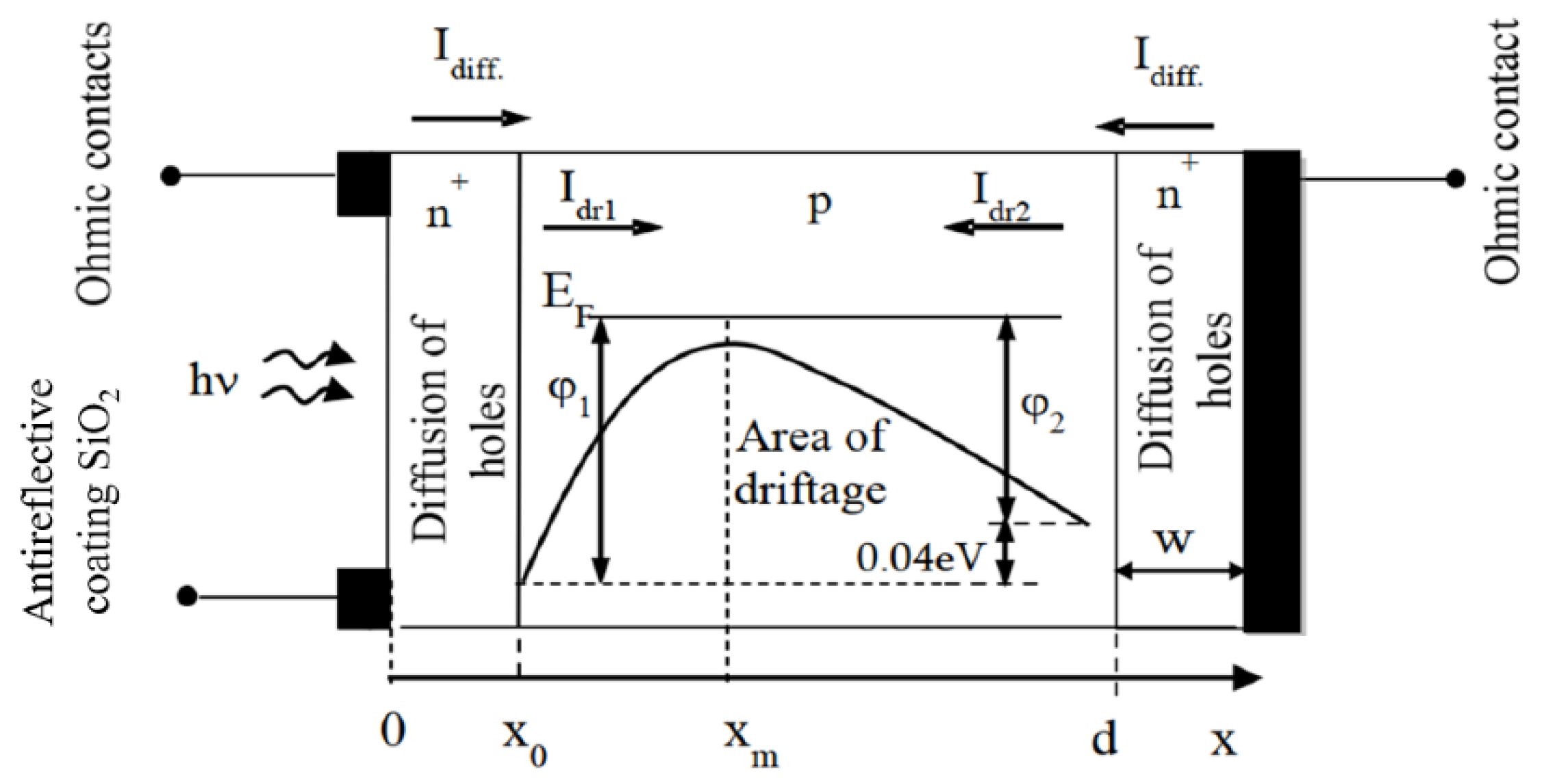
Figure 1. The distribution of the potential energy of holes in the valence band and the direction of the photocurrents.
Photonics 09 00558 g001
Figure 2. The spectral dependence of the photocurrent of DPB photodetector samples at different bias voltages (in mV).
Photonics 09 00558 g002
Figure 3. The change in the spectral photocurrent of DPB photodetector samples sign in the long-wave (a), and short-wave (b), regions at different bias voltages (in mV).
Photonics 09 00558 g003
Figure 4. The dependence of the position of the inversion point of the spectral photocurrent on the photocurrent of the absorbed integral radiation.
Photonics 09 00558 g004
Figure 5. The dependence of the inversion point of the spectral photocurrent on the bias voltage.
Photonics 09 00558 g005
Figure 6. The dependence of the inversion point of the spectral photocurrent on the bias voltage in the short-wave region of the spectrum.
Photonics 09 00558 g006
Figure 7. The measured (a), and experimental (b), spectral distribution of the intensity.
Photonics 09 00558 g007
Figure 8. The spectral dependence of the intensity of the blue (a), green (b), and red (c), LEDs.
Photonics 09 00558 g008
Publisher’s Note: MDPI stays neutral with regard to jurisdictional claims in published maps and institutional affiliations.