Article

Raman Spectroscopy of Graphene/CNT Layers Deposited on Interdigit Sensors for Application in Gas Detection

by
Stefan-Marian Iordache
1,
Ana-Maria Iordache
1,
Ana-Maria Florea (Raduta)
1,
Stefan Caramizoiu
1,
Catalin Parvulescu
2,
Flaviu Baiasu
3,4,
Irina Negut
4,* and
Bogdan Bita
1,3,*
1
Optospintronics Department, National Institute of Research and Development for Optoelectronics-INOE 2000, 409 Atomistilor, 077125 Magurele, Romania
2
National Institute of Microtechnologies, Erou Iancu Nicolae, No. 126A, P.O. Box MG 07, 077190 Voluntari, Romania
3
Department of Electricity, Solid-State Physics and Biophysics, Faculty of Physics, University of Bucharest, 405 Atomistilor, 077125 Magurele, Romania
4
National Institute for Laser, Plasma and Radiation Physics, 409 Atomistilor Street, P.O. Box MG 36, 077125 Magurele, Romania
*
Authors to whom correspondence should be addressed.
Submission received: 6 December 2024 / Revised: 10 January 2025 / Accepted: 17 January 2025 / Published: 20 January 2025
(This article belongs to the Special Issue New Advances in Graphene Synthesis and Applications)

Abstract

:
Graphene/CNT layers were deposited onto platinum electrodes of an interdigitated sensor using radio-frequency magnetron sputtering. The graphene/CNTs were synthesized in an Argon atmosphere at a pressure of (2 × 10⁻²–5 × 10⁻³) mbar, with the substrate maintained at 300 °C either through continuous heating with an electronically controlled heater or by applying a −200 V bias using a direct current power supply throughout the deposition process. The study compares the surface morphology, carbon atom arrangement within the layer volumes, and electrical properties of the films as influenced by the different methods of substrate heating. X-ray diffraction and Raman spectroscopy confirmed the formation of CNTs within the graphene matrix. Additionally, scanning electron microscopy revealed that the carbon nanotubes are aligned and organized into cluster-like structure. The graphene/CNT layers produced at higher pressures present exponential I–V characteristics that ascertain the semiconducting character of the layers and their suitability for applications in gas sensing.

Graphical Abstract

1. Introduction

During the last 20 years, legislation has fostered a huge demand for the use of sensors in medical and environmental technologies for monitoring toxic gases and vapors found in air or contaminants present in waters and rivers (due to industrial effluents and runoff from agriculture fields). As sensing layers, nanostructured carbon sheets, graphene sheets, carbon nanoflakes, carbon nanotubes (CNT), and single-wall carbon nanotubes (SWNT) are of high interest for gas energy storage [1], electronics [2], and sensing applications [3,4,5,6,7,8] due to their resistance to oxidation and high electrical conductivity [9].
Moreover, the major interest in carbon-based structures, graphene, and graphene/CNT composites is attributed to their tunable bandgap and chemical stability [10]. Basically, when these materials cover sensor electrodes, they increase the detection limit of sensor devices [3]. The high thermal and electrical conductivity as well as their superior electron mobility or lightweight characteristics make graphene a very attractive material. Usually, a high thermal conductivity involved in heat transfer implies the low energy of phonons. Graphene exhibits an ambipolar electric field effect such that charge carriers can be tuned continuously between electrons and holes [11,12].
Graphene and CNT films are produced or grown on different substrates by various techniques such as arc discharge, chemical vapor deposition, laser ablation, microwave-plasma-enhanced chemical vapor deposition [13], or magnetron sputtering (MS), in the presence [14] or absence of a catalyst as a function of the desired properties of carbon-based layers [12]. To the best of our knowledge, up until now, only carbon nanoflakes [15], and graphene layers [16] have been synthesized by MS techniques.
MS is a deposition method based on the physical interaction between the substrate and species sputtered from a target. It is known that the energy of sputtered ions/atoms increases the temperature of the substrate similar to a heating source [17,18]. This way, the substrate reaches a temperature of up to 100 °C during the plasma deposition process, and these temperatures could favor the formation of ordered and crystalline structures. It has been reported that the substrate bombardment with ions and energetic atoms produced in plasma during the deposition process can heat the substrate to ~200 °C [19].
In this study, we report the coating of platinum (Pt) interdigitates with graphene/CNT films in radio frequency (RF) MS discharges starting from a graphite target in pure Ar atmosphere. The experiments were performed at different experimental conditions in low and high pressure, either heating the substrate holder by using an electronically controlled heater or by negative electrical biasing of the substrate holder at hundreds of volts. We also identified the influence of temperature and bias potential of the substrate on the morphological and structural properties of graphene/CNT layers.

2. Materials and Methods

2.1. Materials

A graphite sputtering target (99.99% purity, K.J. Lesker Company, Dresden, Germany) with a diameter of 2 inches and a thickness of 2 mm was used for the deposition of graphene/CNT layers in the magnetron sputtering discharge. The interdigitated architecture of the sensors was created through multiple depositions of SiO2, Ti, and Pt layers using plasma-enhanced chemical vapor deposition and MS. The Ti and Pt targets, both with a diameter of 1 inch and 99.999% purity, were obtained from FHR Company (Ottendorf-Okrilla, Germany). The Si substrates used had dimensions of (2 × 2) cm2, are <100>-oriented, and exhibit p-type electrical conductivity.

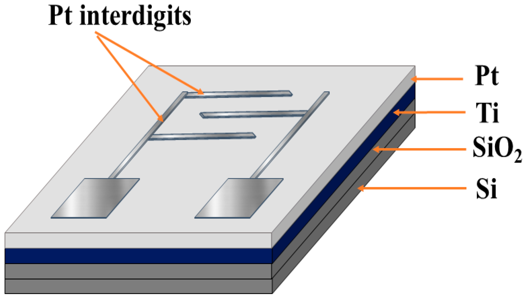
2.2. Formation of the Interdigital Si/SiO2/Ti/Pt Sensor

The initial step involved the deposition of a thin SiO2 layer onto a silicon (Si) substrate. This layer acts as a crucial insulating buffer that prevents electrical interference between the substrate and subsequent layers. Plasma-enhanced chemical vapor deposition (PECVD) was used for this process, chosen for its ability to produce high-quality, uniform SiO2 films at relatively low temperatures, which is essential for preserving the underlying silicon structure.
Following the SiO2 layer, a 5 nm titanium (Ti) buffer layer was deposited onto the Si/SiO2 surface. The purpose of this Ti layer is to enhance the adhesion of the subsequent platinum (Pt) layer to the substrate. This deposition was carried out using MS, a technique well suited for creating thin, uniform metallic layers with strong adhesion properties [20].
After depositing the Ti buffer layer, a solid platinum (Pt) film with a thickness of 283 nm was deposited on top. This Pt layer serves as the primary conductive material for the sensor’s electrodes. A mask was used during the Pt deposition to create interdigitated electrodes, a design that increases the electrode surface area and enhances the sensor’s sensitivity and performance. The Ti and Pt layers were deposited using a Cressington 108 auto/SE system, a specialized piece of equipment that provides precise control over the deposition conditions. The deposition parameters were carefully set to ensure optimal film quality: a working pressure of 0.6 Pa, a current of 40 mA, a voltage of 220 V, and a deposition time of 24 min. These settings were selected to achieve the desired thickness and uniformity of the Ti and Pt layers.
Before the Pt layer was deposited, the SiO2/Ti substrates underwent a thorough cleaning process to remove any contaminants that could affect the quality and adhesion of the Pt layer. The cleaning involved ultrasonic treatment in acetone, methanol, and deionized water for 10 min each, followed by drying with a nitrogen (N2) stream to prevent any moisture or residue remaining on the substrate. Maintaining a clean substrate surface is critical for ensuring strong adhesion of the Pt layer and the overall performance of the sensor.
The entire deposition process was conducted in a vacuum chamber with a pressure maintained at 6 × 10⁻³ Pa. This low-pressure environment is essential for preventing contamination and ensuring that the deposition process is not influenced by air or moisture, leading to high-quality film formation.
The result of these deposition steps is the formation of the interdigital Si/SiO2/Ti/Pt sensor architecture, as shown in Figure 1. This architecture is designed to optimize the sensor’s electrical performance and durability.

2.3. Deposition of Graphene/CNT Layers

In the following, we present the detailed steps and experimental conditions used in the synthesis of graphene/CNT layers. These steps outline the key parameters and methodologies employed to achieve the desired structural and morphological characteristics of the deposited thin films on Si/SiO2/Ti/Pt sensor electrodes and Si substrates.
Graphene/CNT layers have been synthesized using radio-frequency magnetron sputtering (RF MS) in an Argon (Ar) gas atmosphere. The depositions were performed on the surfaces of Si/SiO2/Ti/Pt sensor electrodes and Si substrates, creating conductive and structurally integrated layers suitable for advanced sensor applications.
The RF power was set to 140 W, providing the energy necessary to ionize the Ar gas and sustain the sputtering process. This power level is critical for the efficient ejection of carbon atoms from the graphite target. Two different Ar gas pressures were used during the experiments: 5 × 10⁻³ mbar and 2 × 10⁻² mbar. These pressures were carefully selected to control the mean free path of the sputtered atoms and the overall deposition rate. The base pressure before introducing the Ar gas was maintained at approximately 10−5 mbar to ensure a clean environment, minimizing contamination during the deposition process. The Ar gas flow was maintained at 2 mln/min to create a stable plasma environment, ensuring consistent deposition conditions throughout the 2 h process. The distance between the magnetron source head and the substrate holder was set at 8.5 cm, which was optimized to achieve uniform film deposition across the substrate surface.
Substrates were either placed on a substrate holder heated to 300 °C or on a substrate holder biased at −200 V. These two conditions were employed to study the effects of thermal energy versus electrical bias on the growth and morphology of the graphene/CNT layers. The heated substrate holder was controlled by a homemade oven, which was electronically regulated from outside the vacuum chamber. This setup allowed precise temperature control, ensuring the substrate temperature was consistently maintained at 300 °C. The substrate temperature was confirmed by a thermocouple, which measured 300 °C at the surface of the oven under vacuum conditions before deposition began.
When the substrate holder was at a floating potential during RF MS discharge, a temperature of approximately 230 °C was measured on the substrate surface. This temperature was influenced by the RF power and the Ar gas pressure, providing sufficient thermal energy to facilitate the formation of graphene domains.
For samples on the biased substrate holder, a −200 V bias was applied by connecting the substrate holder to an external electrical power supply. This biasing creates an electric field that influences the trajectory and energy of the sputtered carbon atoms, impacting the growth dynamics of the graphene/CNT layers.
The combination of RF discharge and substrate biasing was utilized to explore the effects on the structural arrangement of the carbon species, particularly in the formation of CNTs and graphene sheets.
Details of the experimental setup, including the specifics of the RF MS discharge system and substrate configurations, have been previously documented in the literature [21]. This prior work provides a foundation for understanding the setup and the rationale behind the chosen deposition parameters.
In Table 1, we present the sample codes for the experimental parameters used.

2.4. Characterization Methods

The RAMAN spectra were acquired by using a LABRAM HR 800 SPECTROMETER (Horiba Jobin Yvon, Lille, France) with a confocal microscope. The excitation radiation of the Ar ion laser was 514.5 nm operating at 1.4 ± 0.05 mW. Through a 100X objective lens, the laser beam was directed to the sample. Spectra were collected for 150 s with a step size of 10 s in the spectra range of 100–4000 cm−1. All measurements were carried out at room temperature. Appropriate fits to the experimental data were achieved utilizing a Gaussian curve-fitting methodology within the OriginLab v.2017 software. The quality of the fittings was demonstrated by a χ2 value of less than 1. The fitting was conducted without constraining or restricting the range of any spectral parameter during the iterative process.
The crystallographic structure of the graphene layers was performed by X-ray diffraction (XRD) on a benchtop Bruker D2 Phaser in a Bragg–Brentano (ϴ-ϴ) geometry, equipped with an ultra-fast LYNXEYE-1D detector. Mono-chromatic CuKα1 radiation (λ = 1.5406 Å) was used for data collection from the intensity of scanned angles in the 14–60° 2ϴ range, with a step size of 0.1°.
The morphological features of graphene/CNT layers were investigated by using an Apreo S ThermoFisher (Waltham, MA USA) scanning electron microscope (SEM), having a maximum resolution of 0.7 nm. SEM micrographs were acquired in top-view and cross-section modes, at a working voltage of 15 kV and pressure of 3 × 10⁻³ Pa.
Electrical and gas testing measurements were performed at room temperature by using a Keithley 2400 multimeter and a computer-controlled Keithley 6517a electrometer using the LabView software ver. 7.1 (Virtual Instrumentation Program). The recording of the direct voltages (I–V) characteristics on the graphene/CNT layers deposited on Pt interdigitates was performed in the range of −0.5–0.5 V, directly on the platinum pad.
For gas sensing measurements both direct and reverse voltage (I–V) characteristics were obtained in the range −1 V–1 V, where contacts were placed on the platinum pads (Pt).

3. Results

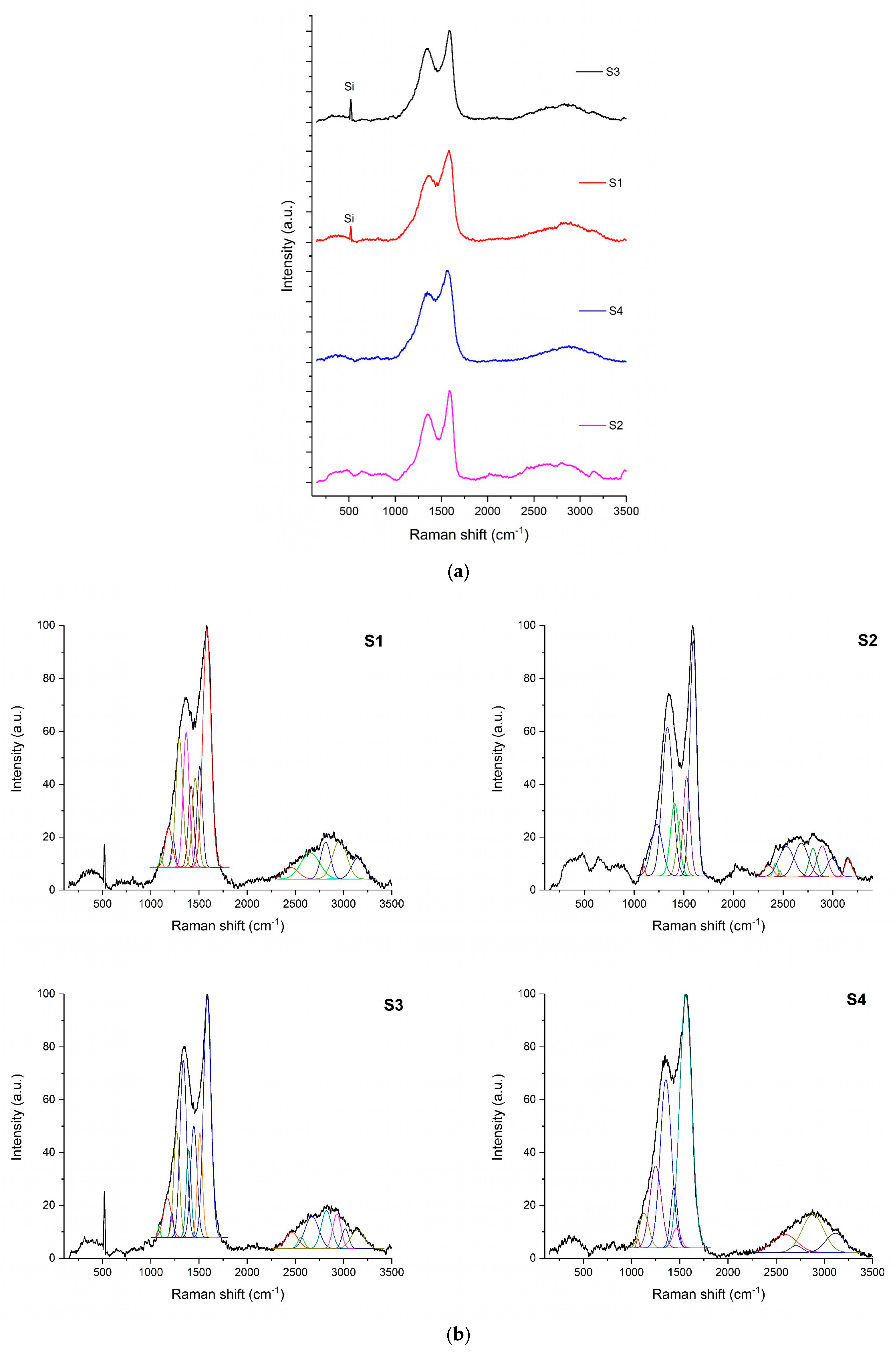
3.1. Raman Spectroscopy Analysis

The Raman spectra of MS-synthesized graphene/CNT layers are presented in Figure 2. The D (1330–1380 cm−1) and G (1560–1600 cm−1) bands characteristic to graphene/CNT structures appear at 1356–1367 cm−1 (S1 and S4) and 1582 cm−1 (S1), respectively, and 1561 cm−1 (S4) (see Figure 2b) [13,22,23,24,25]. The peak found at 1582 cm−1 corresponds to the optical phonon modes of E2g symmetry in crystalline graphite with sp2 C-C bonding structure indicating graphene structures [13,22]. The defects in the graphene plains (due to disorders of graphite crystal size, vacancies, or graphene sheet distortions) are signaled by the D band centered at 1356–1367 cm−1. For all the analyzed samples (see Figure 2), the D and G bands appear in the same wavenumbers range.
The 2D band centered at ~2682 cm−1 (S2) (see Figure 2b) indicates the double resonance of the pie bond being an overtone of the D band [13,22,24,25]. The band from ~2881 cm−1 (S4) (see Figure 2b) represents an overtone combination of D and G bands [13]. Similar peak positions of D, G, 2D, and overtones of D and G bands in Raman spectra were previously reported for the graphene/CNT structures [25,26].
The ratio between the intensity of D and G bands, namely ID/IG gives an estimation of the defects formed in the graphene layers (Table 2). Moreover, the I2D/IG ratio depends on the number of graphene layers. An ID/IG ratio of less than 1 across all samples indicates the presence of multilayer graphene with relatively low defect density [13,22,27]. From the Raman spectra presented in Figure 2, the values of ID/IG were calculated and are under the unit, suggesting the formation of multilayered graphene which is not completely full of defects [13,27].
When analyzing graphene-based structures by Raman spectroscopy, resonance effects enable the identification of carbon nanotube formation and structural differentiation. The high resolution of Raman spectroscopy analysis makes possible the differentiation between graphene-based structures. Also, including the characteristic D, G, and 2D bands and their intensity ratios, we conclude that the layers generated at high pressure in the RF MS discharge predominantly contain multi-walled carbon nanotubes (MWNTs), with structural features indicative of well-aligned and semiconducting behavior.

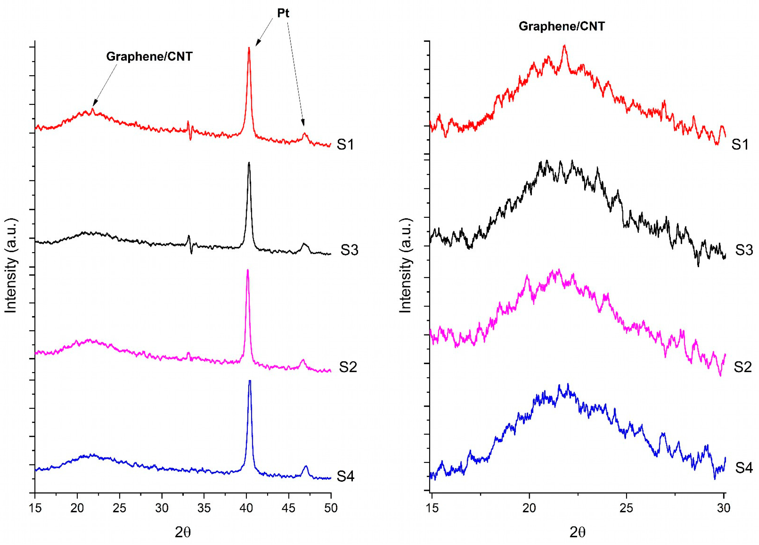
3.2. X-Ray Diffraction Analysis
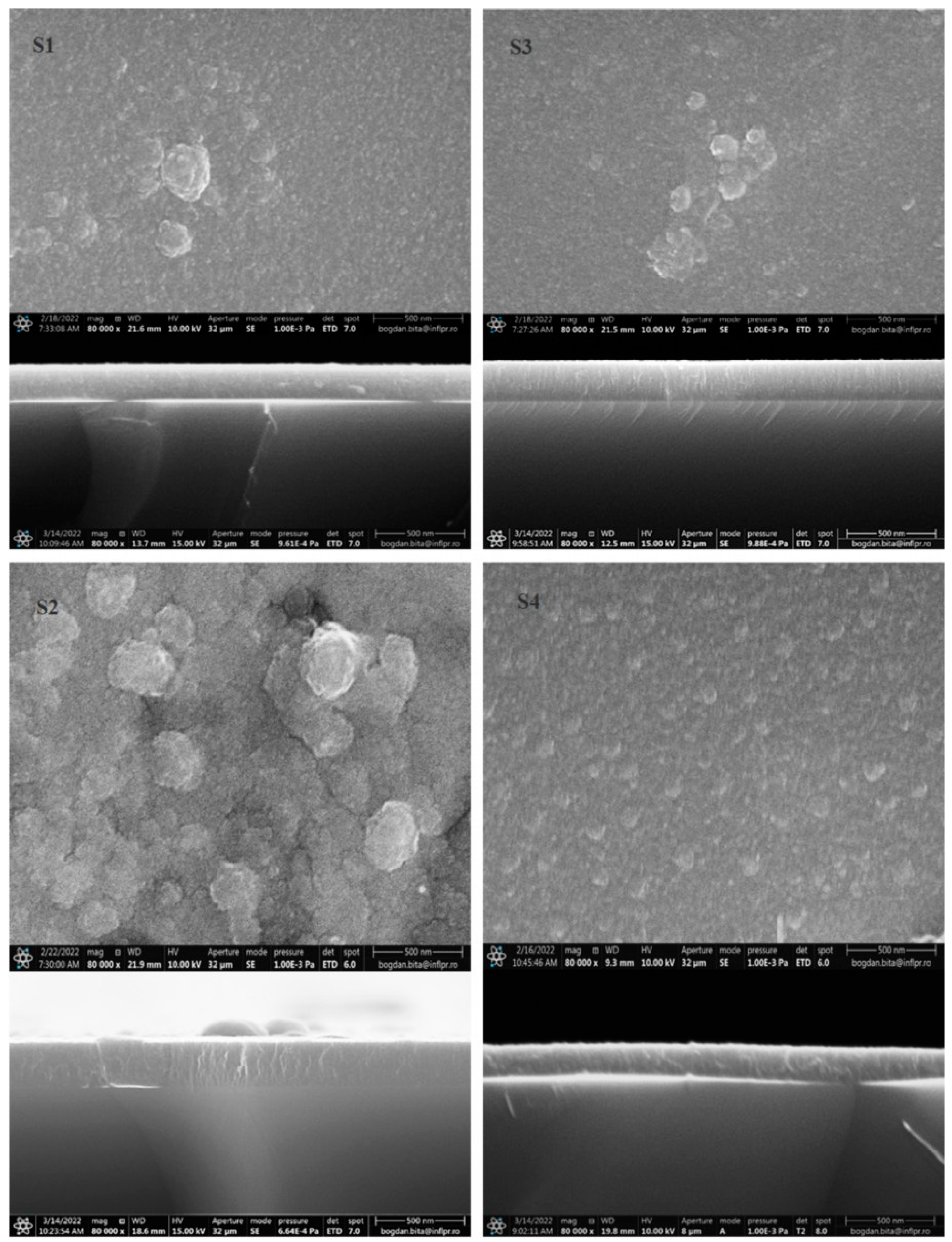
Taking into account that X-ray diffraction analysis discloses the local and global features of microstructure lattice, crystalline phases, and impurities, it is worthwhile to highlight the use of this technique to reveal carbon nanotube formation.
We have analyzed graphene/CNT layers deposited both on sensor electrodes and Si substrates by XRD. The typical peak of the graphene/CNT layers generated in the RF magnetron discharges is identified at ≈26.0°. This peak represents the characteristic graphitic peak [28] arising due to the tubular structure of the carbon atoms in the (002) planes (see Figure 3). The XRD pattern of all the analyzed samples presents the peak from ~26.0° that ascertained the CNT formation.

3.3. SEM-Analysis

The morphology of graphene/CNT layers grown on the surfaces of sensor electrodes and Si substrates was systematically investigated, focusing on key deposition parameters: substrate holder temperature, substrate bias voltage, and Ar working gas pressure.
Figure 4 (S2 and S4) illustrate the impact of substrate heating (using the two methods described in Section 2.3) on the growth patterns of graphene/CNT layers deposited on Si substrates. At a gas pressure of 2 × 10⁻² mbar, the films grown at a substrate temperature of 300 °C (Figure 4, S2) form a more compact, cluster-like structure compared to those grown on a substrate biased at −200 V (Figure 4, S1). This compact morphology can be attributed to the thermal energy provided by substrate heating, which facilitates the alignment and bonding of carbon atoms into organized graphene/CNT domains [11]. When the gas pressure is lower and the substrate is consistently heated to 300 °C throughout the deposition process, the clusters exhibit a more uniform and homogeneous growth across the substrate surface (Figure 4, S4).
Interestingly, no significant differences were observed in the surface morphology of the films deposited at a substrate bias voltage of −200 V at either working gas pressure (Figure 4, S1 and S3). However, the SEM images (Figure 4, S3) reveal disorganized and sparse structures. The lower pressure combined with biasing does not provide the necessary conditions for carbon atoms to assemble into dense, compact formations. SEM images at lower pressures of 5 × 10⁻³ mbar (Figure 4, S4) show uniform, though slightly less dense, clusters compared to high-pressure heating conditions. This can be due to the higher energy of sputtered particles at low pressures, which increases mobility but reduces the deposition rate, resulting in thinner layers.
Previous studies, including our own, have reported that particle energy in RF magnetron discharges is higher at lower pressures [21,29]. Dreghici et al. [17] measured the electron temperature in Ar RF magnetron plasma for a dielectric sputtering target and identified a temperature difference of about 1 eV between samples obtained at pressures of 5 × 10⁻³ mbar and 2 × 10⁻² mbar. Based on these observations, we believe that heating the substrate with an electronically controlled heater promotes the formation of a denser and more compact graphene/CNT cluster-like structure compared to the case where the substrate is biased at −200 V (Figure 4, S1 and S3). Additionally, it is worth noting that in the absence of external heating or biasing of the substrate, we did not observe the formation of graphene or graphene/CNT layers; instead, only diamond-like carbon structures were identified.
Porous and three-dimensional graphene architectures have been reported to exhibit superior gas adsorption properties due to their ability to trap gas molecules within the inter-connected voids and enhance the interaction with the sensing material. For instance, a study discusses the advantages of similar porous architectures in improving gas detection performance, particularly for low-concentration analytes [30].
The SEM cross-sectional images of the films (see Figure 4, positioned below the corresponding top-view SEM images) show that films deposited with heating exhibit a more cohesive structure with well-integrated carbon layers. Heating provides sufficient energy for carbon atoms to form compact, ordered clusters. The thermal energy aids in reducing defects and enhancing the growth of graphene and CNT domains, especially at higher pressures.
Biasing alone is less effective in promoting compact and aligned growth. The resulting films have a more porous and irregular morphology, limiting their performance in applications requiring high-density carbon structures.
The most ordered and aligned graphene/CNT films were observed at a pressure of 2 × 10⁻² mbar when the substrate holder was heated to 300 °C (sample S2, Figure 4). This condition appears to be optimal for promoting the orderly growth of the graphene/CNT structures.
In the absence of reactive gases or catalysts, the growth mechanism can be described as follows: carbon species reaching the substrate initially condense to form nanoislands, which further develop into disordered graphene/CNT films. On heated substrates, these carbon structures tend to arrange themselves into graphene domains or sheets. The size and density of the graphene structures, as well as the formation of CNTs, are highly dependent on the deposition parameters, such as temperature, pressure, and substrate biasing.
The described growth mechanism is consistent with established models where carbon atoms, under the influence of heat and plasma conditions, self-assemble into ordered structures, leading to the formation of graphene and CNTs [31].

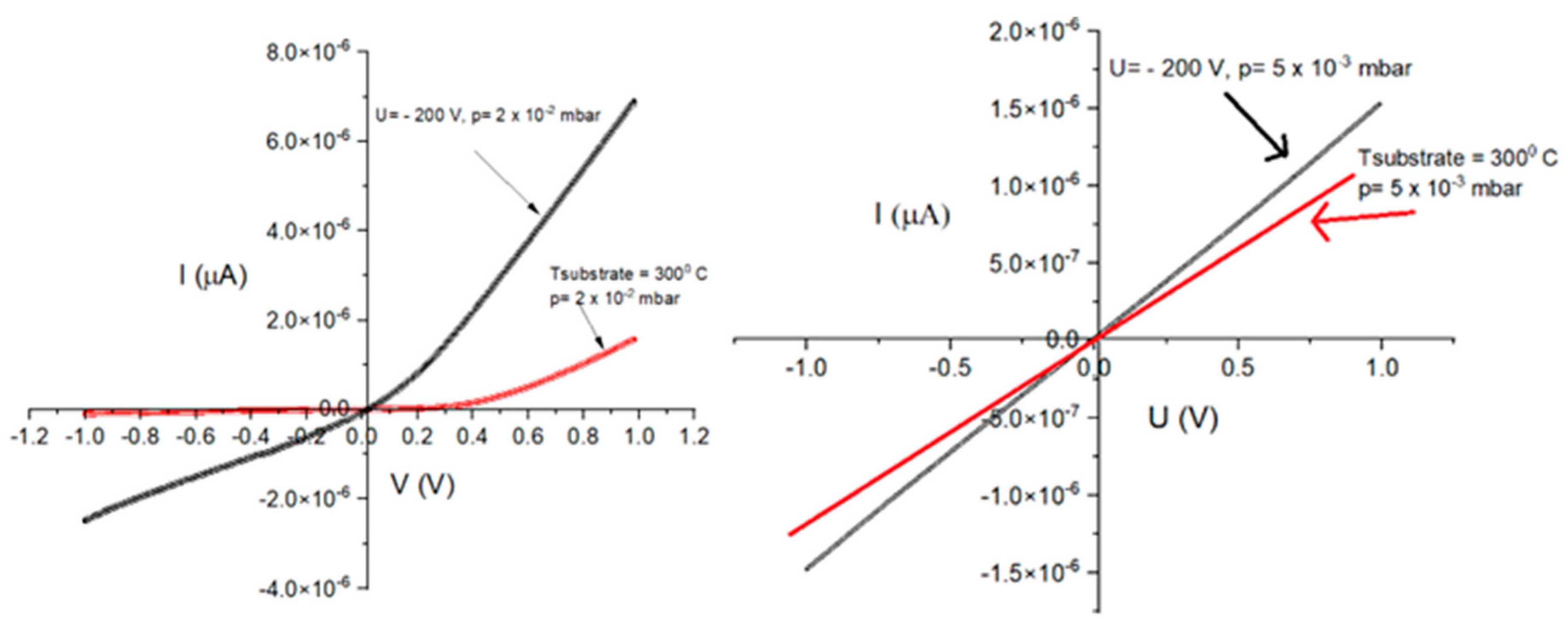
3.4. Electrical and Gas Testing Measurements

Electrical measurements validate whether the graphene/CNT films possess the necessary conductive properties for sensing. These films need to have precise electrical responses to environmental stimuli, such as gases or chemicals. The study’s use of I–V characteristics is crucial for confirming the material’s responsiveness to changes in voltage, which directly correlates with its ability to function as a sensor. This is particularly important because sensor functionality relies on the material’s ability to convert physical or chemical changes into measurable electrical signals [32].
The electrical behavior of the graphene/CNT layers deposited on Pt sensor electrodes was evaluated by measuring the current-voltage (I–V) characteristics at room temperature. A linear I–V characteristic behavior usually indicates semi-conductor behavior across the graphene/CNT film. The formation of a semiconducting CNT in contact with graphene results in an exponential behavior of the I–V characteristic. Such semiconducting behavior of the thin films reveals an ordered carbon structure with a relatively low density of defects [33]. The interdigit had no electrical response because it represents the collector electrode. Without the graphene/CNT thin film, the Pt interdigit electrodes are essentially isolated from each other, meaning there is no continuous path for electrical current to flow between them. In other words, the electrodes alone do not conduct electricity because there is no conductive material connecting them.
The differentiation between semiconducting and metallic behavior in CNTs, as identified through I–V curves, is fundamental. Semiconducting CNTs allow for controlled electrical conductivity changes under different conditions, which is a key requirement in sensors that need to detect minute changes in the environment [34]. This is consistent with findings from previous studies, where semiconducting CNTs were shown to enhance the sensitivity of sensors to gases like nitrogen dioxide [35].
In Figure 5, one can observe that the behavior of the I–V measured on graphene/CNT layers deposited on Pt electrodes in RF MS discharge. Our study showed that films deposited at higher pressures (2 × 10⁻² mbar) exhibited semi-conducting behavior, which could be crucial in applications requiring high sensitivity. Tuning the deposition conditions to achieve specific electrical properties enables the fine-tuning of sensors for different sensing applications. For the case of graphene/CNT layers deposited on Pt electrodes at low pressure (5 × 10⁻³ mbar), the I–V characteristics are found to be linear, indicating a metallic behavior of the CNT.
The electrical properties are often linked with the material’s morphology. For example, in the study, we observed that more compact and aligned CNT structures (as seen in SEM images) contributed to better semiconducting behavior. This highlights the importance of achieving the right morphology for optimal electrical performance in sensors. This is supported by other research that shows a strong correlation between the alignment of CNTs and the enhancement of sensor performance due to improved electron mobility [33,36].
Electrical measurements also bridge the gap between material development and real-world sensor applications. By demonstrating reliable electrical behavior, the graphene/CNT films can be confidently proposed for use in practical sensing devices, such as those monitoring air quality or detecting harmful substances in industrial settings [37].
Electrical measurements are also essential to assess the stability and repeatability of the sensor’s performance over time. A material that shows consistent I–V characteristics under repeated measurements is more likely to perform reliably in real-world applications [38].
Understanding the electrical behavior also helps in designing energy-efficient sensors. For example, semiconducting CNTs typically operate at lower power levels, which is advantageous for sensors that need to run continuously over long periods [39,40].
Extreme voltages, whether excessively high or low, can significantly influence the sensing performance and durability of graphene-based sensors. High voltages may cause irreversible damage to the graphene/CNT interfaces, leading to structural or electrical degradation. Conversely, low voltages may result in insufficient signal-to-noise ratios, compromising the detection capabilities.
Incorporating optimization strategies, such as those involving the use of response surface methodology or computational models, can help identify optimal voltage ranges that ensure both stability and sensitivity. For example, a study demonstrated that applying controlled gate voltages to graphene field-effect transistors improved their sensitivity to ammonia gas, with specific voltage levels significantly enhancing the response and recovery times [41].
Furthermore, studies on graphene-based electronic sensors highlight the importance of voltage optimization for ensuring consistent device behavior under varying environ-mental conditions [42]. Similarly, current-voltage characteristics have been used as a basis for developing models to predict the performance of graphene-based biosensors and gas sensors [43].
Below, one can observe the graph resistance behavior of a graphene/CNT gas sensor over time, with NO2 gas exposure (Figure 6). The plot shows the resistance fluctuating due to a com-bination of sinusoidal variations and random noise, mimicking the dynamic interaction of the sensor with its environment and gas exposure.
The graphene/CNT composite films exhibit remarkable electrical and semiconducting properties, aligning with their potential applications in sensing technologies. The calculated conductivity of 4.2 × 10⁷ S/m highlights the exceptional ability of these films to con-duct electric current, a critical feature for sensors requiring efficient signal transduction.
This high conductivity stems from the unique structure of graphene and CNTs, which provides minimal electron scattering pathways.
The carrier mobility of 2500 cm2/V further emphasis the efficiency of charge carrier movement within the material. Such a high mobility is indicative of superior electron transport dynamics, which is essential for maintaining sensor response speed and accuracy. These values are characteristic of high-performance materials used in advanced electronic and sensing devices.
Additionally, the estimated band gap of 0.12 eV aligns with the semiconducting behavior observed in carbon nanotubes and graphene-based materials. This small band gap allows the material to exhibit both high conductivity and sensitivity to external stimuli, such as the presence of target gases in sensing applications.
Together, these properties confirm that the graphene/CNT composite films are highly suitable for integration into gas sensing devices, combining high sensitivity, rapid response, and low power consumption. Their performance makes them promising candidates for environmental monitoring, industrial safety, and healthcare applications.
The most ordered and aligned graphene/CNT films were obtained at a pressure of 2 × 10⁻² mbar with the substrate holder heated to 300 °C.

4. Discussions and Future Directions

The significance of graphene/CNT-based gas sensors extends beyond industrial applications. These materials can be engineered to improve selectivity and reduce interference from other gases, addressing a common challenge in gas sensing. This capability is crucial for environmental monitoring, where accurate detection of pollutants like sulfur dioxide (SO2) and nitrogen dioxide (NO2) are essential. Moreover, the flexibility and low power consumption of graphene/CNT sensors make them suitable for portable and wearable devices, potentially revolutionizing personal safety equipment. In healthcare applications, these sensors could provide early detection of harmful gases, improving patient care and workplace safety. The integration of graphene/CNT layers with advanced technologies like optical gas imaging (OGI) cameras could further enhance gas detection capabilities, offering real-time monitoring and visualization of gas leaks. This combination of nanomaterials and imaging technology represents a significant leap forward in hazardous gas detection, promising improved safety measures and environmental protection across various sectors.
It is well documented that graphene/CNT composites are excellent sensing matrices due to their high surface area, conductivity, and active sites for adsorption. However, their inherent lack of selectivity for specific gases arises because their electronic properties are influenced by a wide range of adsorbed molecules, making it challenging to distinguish between different gases.
The lack of specific functional groups or binding sites tailored to particular gases limits their ability to differentiate between analytes. To improve gas selectivity, several strategies can be employed. One approach is functionalization, where specific chemical groups or dopants are incorporated onto the graphene/CNT surface to create selective binding sites for target gases [44]. For instance, metal oxides or polymers with an affinity for certain gases can be used to enhance selectivity. Another method involves the use of hybrid structures, where graphene/CNTs are combined with metal oxide nanoparticles, conducting polymers, or other nanomaterials to introduce selectivity while leveraging the high conductivity and sensitivity of the composite matrix [44].
Additionally, selectivity can be enhanced by employing pattern recognition algorithms. By using an array of sensors with varying degrees of response to different gases, coupled with machine learning or pattern recognition algorithms, selective detection can be achieved through signal analysis [45]. Optimization of deposition parameters, such as adjusting defect density, layer thickness, or alignment, can also indirectly influence selectivity by modifying adsorption dynamics [46,47].
These strategies collectively provide a pathway to address the selectivity limitation and greatly enhance the practical utility of graphene/CNT-based sensors in real-world applications. Future studies will focus on implementing and evaluating some of these approaches to improve gas-specific detection capabilities.
Moreover, RF-MS is a widely used technique in industrial applications, including the fabrication of thin films and sensor structures. While RF-MS is inherently scalable, potential challenges for industrial-scale production include ensuring uniformity across large-area substrates, maintaining process stability over extended runs, and optimizing deposition rates to balance throughput and quality. Additionally, addressing material-specific requirements, such as precise control over graphene/CNT alignment and minimizing defects, may require further refinement of process parameters. These considerations highlight the need for continued optimization and monitoring to ensure consistent performance at an industrial scale.

5. Conclusions

In this study, we have shown that graphene/CNT layers can be synthesized in RF MS discharge when the substrate was externally heated up to 300 °C by using an electronically controlled heater. The SEM analysis shows that CNT are grouped in compact cluster-like structures.
The bias of the substrate at −200 V during the entire plasma deposition process proved to be an alternative method for the production of graphene/CNT layers, even if the CNT structures are not as compact and dense as in the case of those obtained when heating the substrate.
The formation of CNT into the deposited layers has been revealed by the X-ray diffraction and Raman spectroscopy analysis. Moreover, the formation of semi-conducting CNT in the RF MS discharge at 2 × 10⁻² mbar working pressure was also indicated by the Raman spectroscopy analysis.
The graphene/CNT layers produced at higher pressures present exponential I–V characteristics that ascertain the semi-conducting character of the layers and their suitability for applications in sensing applications.
The identification and testing of new applications for graphene/CNT layers, with properties modulated during synthesis and post-plasma treatment, represent cutting-edge approaches in utilizing graphene/CNT layers materials for gas detection, particularly for gases posing significant risks. The ability to control the structural and electronic properties of graphene/CNT layers enhances their potential as highly sensitive and selective gas sensors, which could be critical in applications requiring the detection of hazardous gases with high accuracy.

Author Contributions

Conceptualization, S.-M.I. and B.B.; methodology, I.N.; software, B.B.; validation, S.C., A.-M.F. and B.B.; formal analysis, S.-M.I.; investigation, S.-M.I., B.B. and F.B.; resources, C.P.; data curation, A.-M.I. and I.N.; writing—original draft preparation, S.-M.I.; writing—review and editing, S.-M.I., B.B. and I.N.; visualization, I.N.; supervision, S.-M.I.; project administration, B.B.; funding acquisition, S.-M.I. All authors have read and agreed to the published version of the manuscript.

Funding

This research received no external funding.

Data Availability Statement

Data are available upon request to the corresponding authors in reasonable time frame.

Acknowledgments

S.-M.I. B.B. A.-M.I., S.C., A.-M.F. acknowledges the Core Program with the National Research Development and Innovation Plan 2022–2027, carried out with the support of MCID, project no. PN 23 05 and by the Ministry of Research and Innovation. I.N. acknowledges the support from a grant of the Ministry of Research, Innovation and Digitalization, CNCS -UEFISCDI, project number PN-IV-P8-8.3-ROMD-2023-0060, within PNCDI IV and by the Romanian Ministry of Research, Innovation and Digitalization under the Romanian National Nucleu Program LAPLAS VII—contract no. 30N/2023. All authors thank Andreea Groza for providing the infrastructure and support for the RF-MS depositions.

Conflicts of Interest

The authors declare no conflicts of interest.

References

  1. Cott, D.J.; Verheijen, M.; Richard, O.; Radu, I.; Gendt, S.D.; van Elshocht, S.; Vereecken, P.M. Synthesis of large area carbon nanosheets for energy storage applications. Carbon 2013, 58, 59–65. [Google Scholar] [CrossRef]
  2. Novoselov, K.S.; Geim, A.K.; Morozov, S.V.; Jiang, D.; Zhang, Y.; Dubonos, S.V.; Grigorieva, I.V.; Firsov, A.A. Electric Field Effect in Atomically Thin Carbon Films. Science 2004, 306, 666–669. [Google Scholar] [CrossRef] [PubMed]
  3. Vansweevelt, R.; Malesevic, A.; Van Gompel, M.; Vanhulsel, A.; Wenmackers, S.; D’Haen, J.; Vermeeren, V.; Ameloot, M.; Michiels, L.; Van Haesendonck, C.; et al. Biological modification of carbon nanowalls with DNA strands and hybridization experiments with complementary and mismatched DNA. Chem. Phys. Lett. 2010, 485, 196–201. [Google Scholar] [CrossRef]
  4. Rabchinskii, M.K.; Sysoev, V.V.; Glukhova, O.E.; Brzhezinskaya, M.; Stolyarova, D.Y.; Varezhnikov, A.S.; Solomatin, M.A.; Barkov, P.V.; Kirilenko, D.A.; Pavlov, S.I.; et al. Guiding graphene derivatization for the on-chip multisensory arrays: From the synthesis to the theoretical background. Adv. Mater. Technol. 2022, 7, 2101250. [Google Scholar] [CrossRef]
  5. Iordache, S.-M.; Ionete, E.I.; Iordache, A.-M.; Stamatin, I.; Zoita, N.C.; Sobetkii, A.; Grigorescu, C.E.A. Functionalized Carbon Nanotubes for Chemical Sensing: Electrochemical Detection of Hydrogen Isotopes. Coatings 2021, 11, 968. [Google Scholar] [CrossRef]
  6. Iordache, S.M.; Ionete, E.I.; Iordache, A.M.; Tanasa, E.; Stamatin, I.; Grigorescu, C.E.A. Pd-decorated CNT as sensitive material for applications in hydrogen isotopes sensing—Application as gas sensor. Int. J. Hydrogen Energy 2021, 46, 11015–11024. [Google Scholar] [CrossRef]
  7. Zubarev, A.; Cuzminschi, M.; Iordache, A.-M.; Iordache, S.-M.; Rizea, C.; Grigorescu, C.E.A.; Giuglea, C. Graphene-Based Sensor for the Detection of Cortisol for Stress Level Monitoring and Diagnostics. Diagnostics 2022, 12, 2593. [Google Scholar] [CrossRef]
  8. Iordache, S.-M.; Iordache, A.-M.; Zubarev, A.; Caramizoiu, S.; Grigorescu, C.E.A.; Marinescu, S.; Giuglea, C. Spectro-Electrochemical Properties of a New Non-Enzymatic Modified Working Electrode Used for Histamine Assessment in the Diagnosis of Food Poisoning. Foods 2023, 12, 2908. [Google Scholar] [CrossRef]
  9. Wu, Y.H.; Yu, T.; Shen, Z.X. Two-dimensional carbon nanostructures: Fundamental properties, synthesis, characterization, and potential applications. J. Appl. Phys. 2010, 108, 071301. [Google Scholar] [CrossRef]
  10. Kobayashi, K.; Tanimura, M.; Nakai, H.; Yoshimura, A.; Yoshimura, H.; Kojima, K.; Tachibana, M. Nanographite domains in carbon nanowalls. J. Appl. Phys. 2007, 101, 094306. [Google Scholar] [CrossRef]
  11. Bita, B.; Vizireanu, S.; Stoica, D.; Ion, V.; Yehia, S.; Radu, A.; Iftimie, S.; Dinescu, G. On the Structural, Morphological, and Electrical Properties of Carbon Nanowalls Obtained by Plasma-Enhanced Chemical Vapor Deposition. J. Nanomater. 2020, 2020, e8814459. [Google Scholar] [CrossRef]
  12. Lee, K.-Y.; Ikuno, T.; Tsuji, K.; Ohkura, S.; Honda, S.; Katayama, M.; Oura, K.; Hirao, T. Synthesis of aligned bamboo-like carbon nanotubes using radio frequency magnetron sputtering. J. Vac. Sci. Technol. B Microelectron. Nanometer Struct. Process. Meas. Phenom. 2003, 21, 1437–1441. [Google Scholar] [CrossRef]
  13. Choi, H.; Kwon, S.; Kang, H.; Kim, J.H.; Choi, W. Adhesion-Increased Carbon Nanowalls for the Electrodes of Energy Storage Systems. Energies 2019, 12, 4759. [Google Scholar] [CrossRef]
  14. Sahu, P.K.; Pandey, R.K.; Dwivedi, R.; Mishra, V.N.; Prakash, R. Polymer/Graphene oxide nanocomposite thin film for NO2 sensor: An in situ investigation of electronic, morphological, structural, and spectroscopic properties. Sci. Rep. 2020, 10, 2981. [Google Scholar] [CrossRef]
  15. Guzmán-Olivos, F.; Espinoza-González, R.; Fuenzalida, V. Nanocrystalline carbon flakes deposited by RF magnetron sputtering. Mater. Lett. 2016, 167, 242–245. [Google Scholar] [CrossRef]
  16. Scalese, S.; Scuderi, V.; Privitera, V.; Pennisi, A.; Simone, F. Simultaneous catalyst deposition and growth of aligned carbon nanotubes on SiO2/Si substrates by radio frequency magnetron sputtering. J. Appl. Phys. 2007, 102, 114905. [Google Scholar] [CrossRef]
  17. Dreghici, D.B.; Butoi, B.; Predoi, D.; Iconaru, S.L.; Stoican, O.; Groza, A. Chitosan–Hydroxyapatite Composite Layers Generated in Radio Frequency Magnetron Sputtering Discharge: From Plasma to Structural and Morphological Analysis of Layers. Polymers 2020, 12, 3065. [Google Scholar] [CrossRef]
  18. Ren, X.; Zhu, H.; Liu, N.; Wei, Q.; Pu, J.; Ma, L.; Wang, Y.; Xie, Y.; Wei, B.; Yu, Z.; et al. Hydrogenated diamond-like carbon film prepared by RF bias assisting magnetron sputtering. Mater. Res. Express 2019, 6, 076403. [Google Scholar] [CrossRef]
  19. Shapovalov, V.I.; Komlev, A.E.; Bondarenko, A.S.; Baykov, P.B.; Karzin, V.V. Substrate heating and cooling during magnetron sputtering of copper target. Phys. Lett. A 2016, 380, 882–885. [Google Scholar] [CrossRef]
  20. Manguele, J.J.; Baudouin, F.; Cibert, C.; Domenges, B.; Demange, V.; Guilloux-Viry, M.; Fouchet, A.; Poullain, G. Orientation control of Platinum electrode grown on silicon using [Ca2Nb3O10]–nanosheets as seed layer. Thin Solid Films 2023, 765, 139640. [Google Scholar] [CrossRef]
  21. Groza, A.; Dreghici, D.B.; Ganciu, M. Calcium Phosphate Layers Deposited on Thermal Sensitive Polymer Substrates in Radio Frequency Magnetron Plasma Discharge. Coatings 2019, 9, 709. [Google Scholar] [CrossRef]
  22. Kononenko, O.; Brzhezinskaya, M.; Zotov, A.; Korepanov, V.; Levashov, V.; Matveev, V.; Roshchupkin, D. Influence of numerous Moire superlattices on transport properties of twisted multilayer graphene. Carbon 2022, 194, 52–61. [Google Scholar] [CrossRef]
  23. Tüzemen, E.Ş.; Kilic, M.; Zeyrek, B.K.; Kasapoglu, A.E.; Gür, E.; Alaydin, B.O.; Esen, M.; Esen, R. Formation of carbon nanowalls by pulsed filtered cathodic vacuum arc deposition. Diam. Relat. Mater. 2019, 93, 200–207. [Google Scholar] [CrossRef]
  24. Adhikari, B.; Majumdar, S. Polymers in sensor applications. Prog. Polym. Sci. 2004, 29, 699–766. [Google Scholar] [CrossRef]
  25. Jorio, A.; Saito, R. Raman spectroscopy for carbon nanotube applications. J. Appl. Phys. 2021, 129, 021102. [Google Scholar] [CrossRef]
  26. Lin, C.-C.; Shen, Y.-L.; Wu, A.-N. The Effects of Power Levels/Time Periods for Sputtering Cobalt onto Carbon Nanotubes/Graphene Composites and Cobalt Annealed on the Characteristics of Anode Materials for Lithium-Ion Batteries. J. Nanomater. 2018, 2018, e9489042. [Google Scholar] [CrossRef]
  27. Ionescu, M.I.; Sun, X.; Luan, B. Multilayer graphene synthesized using magnetron sputtering for planar supercapacitor application. Can. J. Chem. 2015, 93, 160–164. [Google Scholar] [CrossRef]
  28. Maniwa, Y.; Fujiwara, R.; Kira, H.; Tou, H.; Kataura, H.; Suzuki, S.; Achiba, Y.; Nishibori, E.; Takata, M.; Sakata, M.; et al. Thermal expansion of single-walled carbon nanotube (SWNT) bundles: X-ray diffraction studies. Phys. Rev. B 2001, 64, 241402. [Google Scholar] [CrossRef]
  29. Surmenev, R.A.; Surmeneva, M.A.; Evdokimov, K.E.; Pichugin, V.F.; Peitsch, T.; Epple, M. The influence of the deposition parameters on the properties of an rf-magnetron-deposited nanostructured calcium phosphate coating and a possible growth mechanism. Surf. Coat. Technol. 2011, 205, 3600–3606. [Google Scholar] [CrossRef]
  30. Chen, Z.; Wang, J.; Cao, N.; Wang, Y.; Li, H.; Rooij, N.F.D.; Umar, A.; Feng, Y.; French, P.J.; Zhou, G. Three-Dimensional Graphene-Based Foams with “Greater Electron Transferring Areas” Deriving High Gas Sensitivity. ACS Appl. Nano Mater. 2021, 4, 13234–13245. [Google Scholar] [CrossRef]
  31. Mao, Y.; Liu, S.; Liu, S.; Wu, G.; Liu, Q.; Du, X. Synergistic effect of CNT and N-Doped graphene foam on improving the corrosion resistance of ZN reinforced epoxy composite coatings. Polymers 2024, 16, 3513. [Google Scholar] [CrossRef]
  32. Mbayachi, V.B.; Ndayiragije, E.; Sammani, T.; Taj, S.; Mbuta, E.R.; Khan, A.U. Graphene synthesis, characterization and its applications: A review. Results Chem. 2021, 3, 100163. [Google Scholar] [CrossRef]
  33. Peng, Z.; Ng, A.L.; Kwon, H.; Wang, P.; Chen, C.F.; Lee, C.S.; Wang, Y. Graphene as a functional layer for semiconducting carbon nanotube transistor sensors. Carbon 2017, 125, 49–55. [Google Scholar] [CrossRef] [PubMed]
  34. Schroeder, V.; Savagatrup, S.; He, M.; Lin, S.; Swager, T.M. Carbon Nanotube Chemical Sensors. Chem. Rev. 2019, 119, 599–663. [Google Scholar] [CrossRef] [PubMed]
  35. Snyder, G.; Toberer, E. Complex thermoelectric materials. Nat. Mater. 2008, 7, 105–114. [Google Scholar] [CrossRef]
  36. Liang, Q.; Yao, X.; Wang, W.; Liu, Y.; Wong, C.P. A Three-Dimensional Vertically Aligned Functionalized Multilayer Graphene Architecture: An Approach for Graphene-Based Thermal Interfacial Materials. ACS Nano 2011, 5, 2392–2401. [Google Scholar] [CrossRef]
  37. Shen, X.; Opulente, D.A.; Kominek, J.; Zhou, X.; Steenwyk, J.L.; Buh, K.V.; Haase, M.A.; Wisecaver, J.H.; Wang, M.; Doering, D.T.; et al. Tempo and Mode of Genome Evolution in the Budding Yeast Subphylum. Cell 2018, 175, 1533–1545.e20. [Google Scholar] [CrossRef]
  38. Kumar, S.; Kolassa, J.; Reichle, R.; Crow, W.; de Lannoy, G.; de Rosnay, P.; MacBean, N.; Girotto, M.; Fox, A.; Quaife, T.; et al. An agenda for land data assimilation priorities: Realizing the promise of terrestrial water, energy, and vegetation observations from space. J. Adv. Model. Earth Syst. 2022, 14, e2022MS003259. [Google Scholar] [CrossRef]
  39. Kong, J.; Franklin, N.R.; Zhou, C.; Chapline, M.G.; Peng, S.; Cho, K.; Dai, H. Nanotube Molecular Wires as Chemical Sensors. Science 2000, 287, 622–625. [Google Scholar] [CrossRef]
  40. Park, S.; Vosguerichian, M.; Bao, Z. A review of fabrication and applications of carbon nanotube film-based flexible electronics. Nanoscale 2013, 5, 1727–1752. [Google Scholar] [CrossRef]
  41. Zhao, M.; Tian, Y.; Yan, L.; Liu, R.; Chen, P.; Wang, H.; Chu, W. Unique modulation effects on the performance of graphene-based ammonia sensors via ultrathin bimetallic Au/Pt layers and gate voltages. Phys. Chem. Chem. Phys. 2023, 25, 19764–19772. [Google Scholar] [CrossRef] [PubMed]
  42. He, Q.; Wu, S.; Yin, Z.; Zhang, H. Graphene-based electronic sensors. Chem. Sci. 2012, 3, 1764–1772. [Google Scholar] [CrossRef]
  43. Karimi, H.; Rahmani, R.; Akbari, E.; Rahmani, M.; Ahamdi, M.T. Optimization of Current-Voltage Characteristics of Graphene-Based Biosensors. In Handbook of Research on Nanoelectronic Sensor Modeling and Applications; Ahmadi, M.T., Ismail, R., Anwar, S., Eds.; IGI Global: Hershey PA, USA, 2017; pp. 244–264. [Google Scholar] [CrossRef]
  44. Xu, J.; Wang, Y.; Hu, S. Nanocomposites of graphene and graphene oxides: Synthesis, molecular functionalization and application in electrochemical sensors and biosensors. A review. Microchim. Acta 2017, 184, 1–44. [Google Scholar] [CrossRef]
  45. Hayasaka, T.; Lin, A.; Copa, V.C.; Lopez, L.P., Jr.; Loberternos, R.A.; Ballesteros, L.I.M.; Kubota, Y.; Liu, Y.; Salvador, A.A.; Lin, L. An electronic nose using a single graphene FET and machine learning for water, methanol, and ethanol. Microsyst. Nanoeng. 2020, 6, 50. [Google Scholar] [CrossRef]
  46. Islam, M.H.; Afroj, S.; Uddin, M.A.; Andreeva, D.V.; Novoselov, K.S.; Karim, N. Graphene and CNT-Based Smart Fiber-Reinforced Composites: A Review. Adv. Funct. Mater. 2022, 32, 2205723. [Google Scholar] [CrossRef]
  47. Jomol, P.J.; Mary Nancy, T.E.; Bindu Sharmila, T.K. A comprehensive review on the environmental applications of graphene–carbon nanotube hybrids: Recent progress, challenges and prospects. Mater. Adv. 2021, 2, 6816–6838. [Google Scholar] [CrossRef]
Figure 1. Architecture of interdigital Si/SiO2/Ti/Pt sensor.
Carbon 11 00009 g001
Figure 2. Raman spectroscopy analysis of graphene/CNT layers (a) and appropriate fits to the experimental data (b).
Carbon 11 00009 g002
Figure 3. X-ray diffraction pattern of graphene/CNT layers deposited on Pt sensor.
Carbon 11 00009 g003
Figure 4. SEM images in top-view and cross-section modes of graphene/CNT films of: S1; S2; S3; S4 samples.
Carbon 11 00009 g004
Figure 5. I–V characteristics for graphene/CNT layers deposited on Pt interdigits.
Carbon 11 00009 g005
Figure 6. Resistance of graphene/CNT gas sensor over the time for NO2 exposure.
Carbon 11 00009 g006
Table 1. Sample codes and the experimental parameters used.
Sample CodeExperimental Parameters
Voltage Bias [U (V)]Temperature [Tsubstrate (°C)]Pressure [P (mbar)]
S1−200RT2 × 10−2
S20300
S3−200RT5 × 10−3
S40300
Table 2. Ratio between the intensity of D and G bands, respectively, 2D and G bands.
SampleID/IGI2D/IG
S10.600.15
S20.610.17
S30.750.16
S40.680.18
Disclaimer/Publisher’s Note: The statements, opinions and data contained in all publications are solely those of the individual author(s) and contributor(s) and not of MDPI and/or the editor(s). MDPI and/or the editor(s) disclaim responsibility for any injury to people or property resulting from any ideas, methods, instructions or products referred to in the content.

