1. Introduction
The rapid advances in technology for the fabrication of miniature electronic devices call for the development of sufficiently small sources and accumulators of energy (on-chip power sources). Micro-fuel cells and supercapacitors are the most viable options for this purpose [
1,
2,
3].
The use of an external oxidizing agent (air) allows for a significant decrease in the size/weight of electrochemical cells; therefore, metal-air batteries (e.g., Zn-air, Li-air, Al-air) [
4,
5,
6] offer a prospective solution in terms of creating autonomous energy sources. In these batteries, charge separation occurs via oxidation of the metal in contact with an electrolyte and reduction of oxygen entering the battery through a porous electrode.
Among other representatives of the class, it is worth mentioning silicon-air (Si-air) batteries based on crystalline silicon (c-Si) wafers [
7,
8,
9,
10]. Due to a four-electron oxidation reaction, their specific energy is 3822 mAh·g
−1, which is on par with that of a Li-air battery (3860 mAh·g
−1) [
10], while their material (silicon) is abundant, non-toxic, and eco-friendly. An essential component of a Si-air or a metal-air battery is an alkaline electrolyte or an ionic liquid containing fluorides (e.g., 1-ethyl-3-methylimidazolium hydrofluoride), which enables charge transfer between electrodes. These electrochemical cells have a considerable thickness (over 1 cm) and, therefore, cannot be considered flexible energy sources.
Great progress has been achieved recently in the field of electrochemical power sources. A lot of developments and investigations have occurred in incorporating different materials, including carbon nanotubes as conductors and electrodes [
11], silicon nanowires as anodes [
12], and cellulose—which is the most abundant renewable polymer source available—as a substrate for electrode materials [
13,
14,
15]. Thus, prominent trends in the research of power sources include miniaturization (introduction of low-scale materials such as nanoparticles or graphene) and the achievement of high flexibility in combination with the abundance, non-toxicity, and eco-friendliness mentioned earlier [
11,
12,
13,
14,
15,
16,
17,
18].
This work deals with the fabrication of an ultra-thin battery composed of a film of silicon nanoparticles encased between two aluminium planar electrodes. The net thickness of such a structure (disregarding the thickness of the substrate) is less than 2 microns, which makes it a perfect candidate for a flexible energy source, assuming that a flexible substrate is used.
Previous investigations of silicon nanoparticles between interdigitated aluminium electrodes [
19] showed a positive effect of water on electrical conductivity, and it was established that oxidation of the surface of Si nanocrystals (nc-Si) diminishes the electrical conductivity of the films irreversibly. However, the advantages of the application of such structure in a humid environment in itself deserves further study. At the same time, the authors of [
19] didn’t observe emf generation, due to the symmetry of electrodes. Asymmetry of the structure is crucial for emf generation. The battery produced in this work is truly an autonomous current source, and is essentially a nc-Si/water element. In the element reported here, the film of silicon nanoparticles works simultaneously as fuel, as a charge transport membrane, and as an electrode separator.
2. Experimental Section
Silicon nanoparticles produced via laser-induced silane pyrolysis [
20] were used to obtain silicon films. The mean diameter of the nc-Si was determined to be 15 nm by means of transmission electron microscopy (TEM). TEM was performed on a JEM2100 microscope (JEOL, Tokyo, Japan) with 200 kV accelerating voltage. The mean size was calculated by averaging of diameters of 100 particles. After storage in air, the surface of nc-Si becomes partially oxidized, and its composition may be described as SiO
x (0 < x < 2).
Fabrication of sandwich structures started with vacuum deposition of a bottom aluminium electrode (denoted later as the bottom contact, see
Figure 1) on a glass substrate. Films of nc-Si were then deposited on the bottom contact by means of either electrophoresis or spin-coating from sols of nc-Si in polar solvents (water or acetone). The procedure was finalized with a vacuum deposition of top aluminium electrodes. A few structures were annealed in vacuum (10
−5 Torr) for 1 h at a temperature of 700 K before the deposition of top aluminium electrodes.
As a result, the cell work area was 1.4 cm2 for each contact. The height of the cell was determined by the glass substrate (1.2 mm). The thickness of the Al contacts (bottom and top) and that of nc-Si film were 0.3 µm and 0.2–0.5 µm, respectively.
To discern the electronic and protonic conductivity, Nafion-containing samples were produced. Nafion is a sulfonated tetrafluoroethylene-based fluoropolymer-copolymer. It is commonly used as a protonic conductor for proton exchange membrane in fuel cells. This structure was manufactured through vacuum deposition of an aluminium electrode on Nafion film, followed by deposition of a film of nc-Si on the other side, and covering it with the top aluminium electrode. This resulted in a flexible structure (without substrate), where the Nafion membrane was between the bottom contact (3) and the film of silicon nanocrystals (2) (see
Figure 1).
The quality of the silicon nanoparticle films was controlled with a scanning electron microscope (SEM) NVision 40 (Carl Zeiss, Oberkochen, Germany) with an acceleration voltage 5 kV and 2 nm resolution. The thickness of the films was determined with use of a TalyStep profilometer (Taylor-Hobbson, Leicester, England).
Emf measurements were carried out in the temperature range of 300 to 400 K. The temperature was registered with an error of 0.1 °C. For signal registration, high-ohmic 24-bit 4-channel digital recorders Expert-001 (Ekoniks, Moscow, Russia) were used. The studies of effects of atmosphere composition on electronic characteristics of the samples were performed in a gas flow chamber allowing pressure, gas composition and humidity control. Relative partial pressures of water vapor and oxygen were determined with HIH 4000 (Honeywell, Lincolnshire, IL, USA) and Oxic 12 sensors (Oxonium, Saint-Petersburg, Russia) to an accuracy of 3.5 and 1%, respectively.
3. Results and Discussion
Initially, the investigation of M/nc-Si/M structures was concerned with the use of nc-Si film as a solid separator and as an electrolyte. Thus, different bottom and top contact materials were considered. With the results obtained, it was found that the change of the material of electrodes didn’t significantly affect emf generation. Moreover, it was established that a more important role in this process is played by water; therefore, we focused our attention on equal-metal structures, and aluminium proved to be the most convenient material.
3.1. SEM Investigation
In
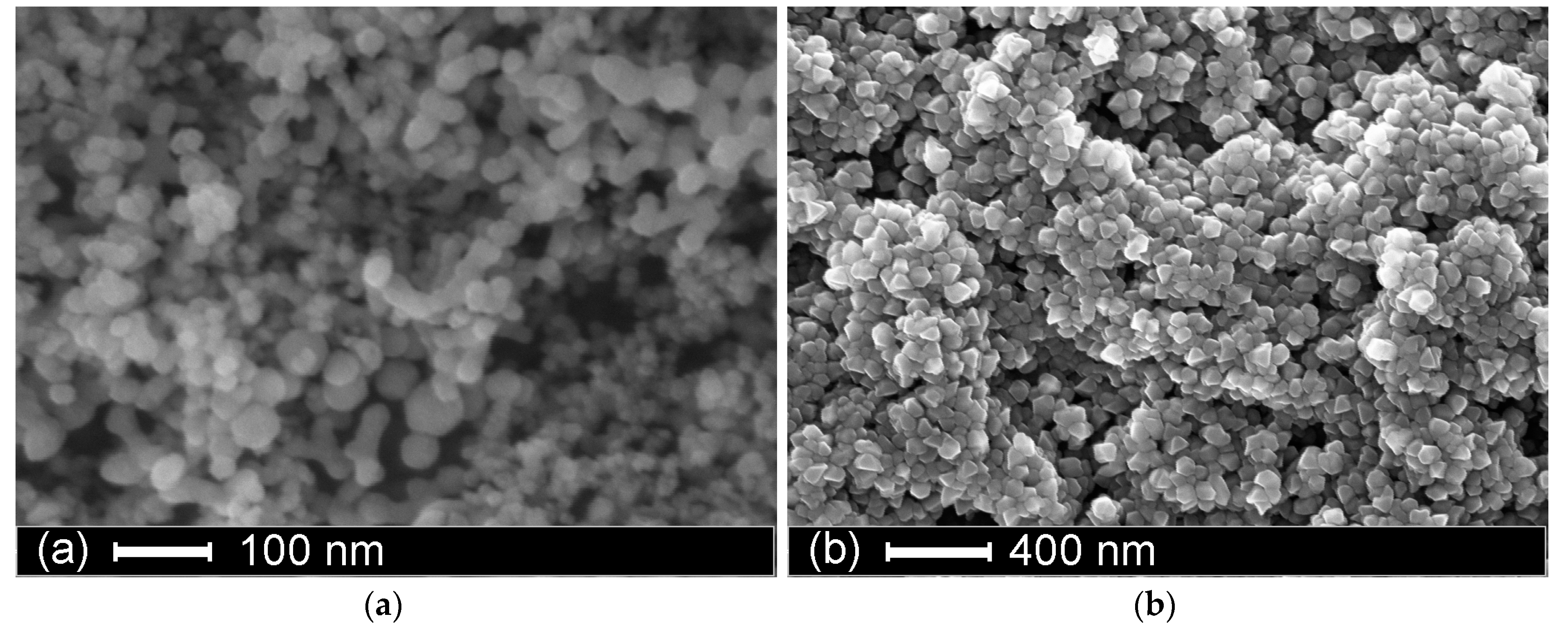
Figure 2, SEM images of the structures without the top electrode (
Figure 2a), and with the aluminium top contact (
Figure 2b) are presented. The top aluminium contact mostly consists of faceted metal nanoparticles with an average size of 75 ± 10 nm.
Evidently, the fabricated material is very porous. Porosity of the top aluminium electrode enables water permeation. Moreover, it was established that this electrode configuration is formed spontaneously during the deposition process.
On the contrary, porosity of nc-Si film may lead to poor charge transfer. In order to mitigate this, some samples were annealed in vacuum before the top aluminium electrode deposition (the conditions are mentioned in the Experimental section). As a result, emf values increased more than two times (see below).
The use of annealing to increase the conductivity of nc-Si films was already known [
21,
22]. Possible mechanisms include sintering, particle transfer, and even sublimation of nanoparticles from a hot substrate to a cold one [
23]. This process makes it possible to increase density and conductivity. Our investigations showed that the thickness of nc-Si films decreased twofold upon annealing at 300 °C for 30 min. After that, the thickness remained constant. No sublimation was observed during this process, and we propose that an increase of nc-Si film density occurs.
3.2. The Influence of Temperature and Humidity on Emf Generation
Methods of nc-Si film deposition (electrophoresis or spin-coating) do not yield significantly different results in terms of the final emf value. The other two parameters are temperature and humidity. Both temperature and humidity have a positive impact on the emf. While they affect charge transfer processes, moisture can also serve as an oxidizer component, which ensures the maintenance of chemical processes.
An investigation of a series of structures in dry Ar/O2 mixtures has shown that the emf increases with the oxygen amount. The growth is not significant—no more than 10 percent after the increase of oxygen from 0 to 100 percent. As the influence of oxygen was even lower when using wet Ar/O2 mixtures, the variation of this parameter wasn’t studied in greater detail.
Every sample studied exhibited a certain potential difference between the top and bottom contacts, with the exact value ranging between 30 mV and 1 V, depending on temperature and humidity. For all samples, the potential difference between the bottom and top contacts was positive. Current that flows from the bottom electrode to the top electrode in external circuit is positive.
3.2.1. Temperature Dependence
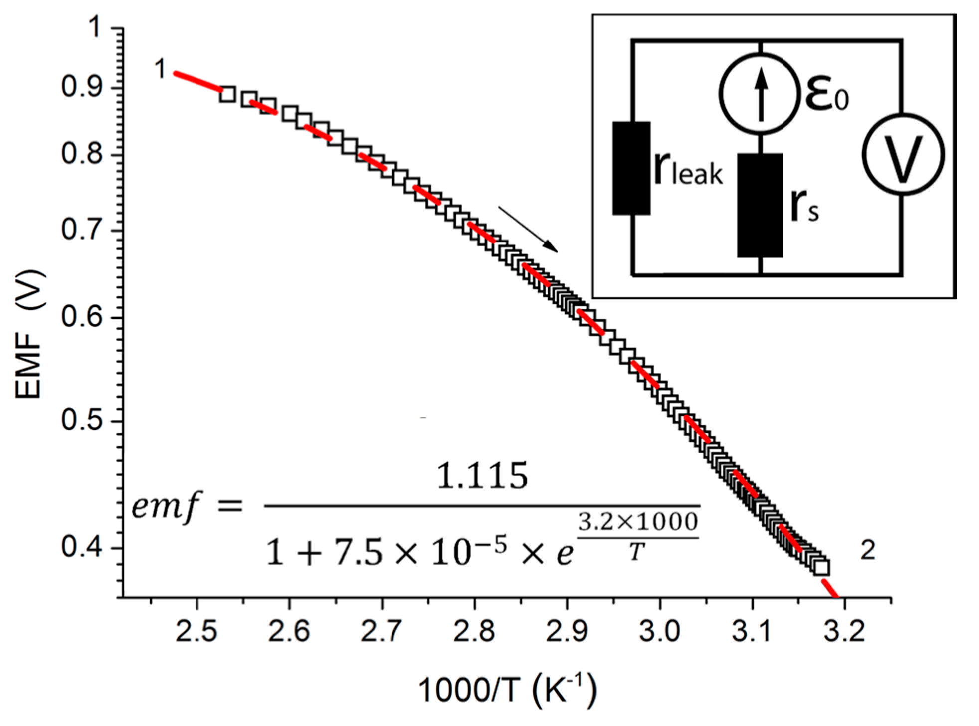
The plotting of temperature-emf curves allows one to formulate a model of emf generation in the structures investigated. In
Figure 3, we present the semi-log plot of the emf generated by the sample in air at constant humidity as a function of reciprocal temperature. The dependence given is characteristic of all structures studied, and isn’t fit well by a single exponent emf ~
e−E/kT, where
E is the activation energy. Therefore, the following model (
Figure 3, insert) is proposed.
The model suggests that there are two charge transfer processes associated with emf generation: one series to the source (possesses an
rs resistance), which is associated with internal charge transfer; and one leak process (
rleak, shunting), which probably appears in contacts of different layers. Activation energies behind these processes (
Es and
Eleak, respectively) differ greatly, because the energy of short circuit tends toward zero. Therefore, the following relation is true:
Es >>
Eleak. This implies that parallel resistance (
rleak) is less dependent on temperature in the studied temperature interval. However, the series process is of activational character, and one can get the emf from the following formula:
taking into account that
r =
r0 ×
eE/kT and neglecting
Eleak:
The values of
Es, r0s/r0leak and ε
0 are fit parameters. The proposed model leads to an accurate approximation of emf dynamics data for the structure, as is shown in
Figure 3. The fit values for this sample are: ε
0 ≈ 1.1 V,
Es ≈ 0.28 eV. According to [
24], there are surface states for Si that are situated inside the band gap 0.5 eV below the bottom of the conduction band. This value is close to
Es, and we suppose that injection of electrons happens through these states with consequent thermal activation in the conduction band.
From the analysis of the temperature dependences of the emf, it follows that dissipative processes occur in these structures, in parallel with the process of emf generation. Obviously, such processes shunt the emf, and lead to a decrease in its effective value. To find
r0 and
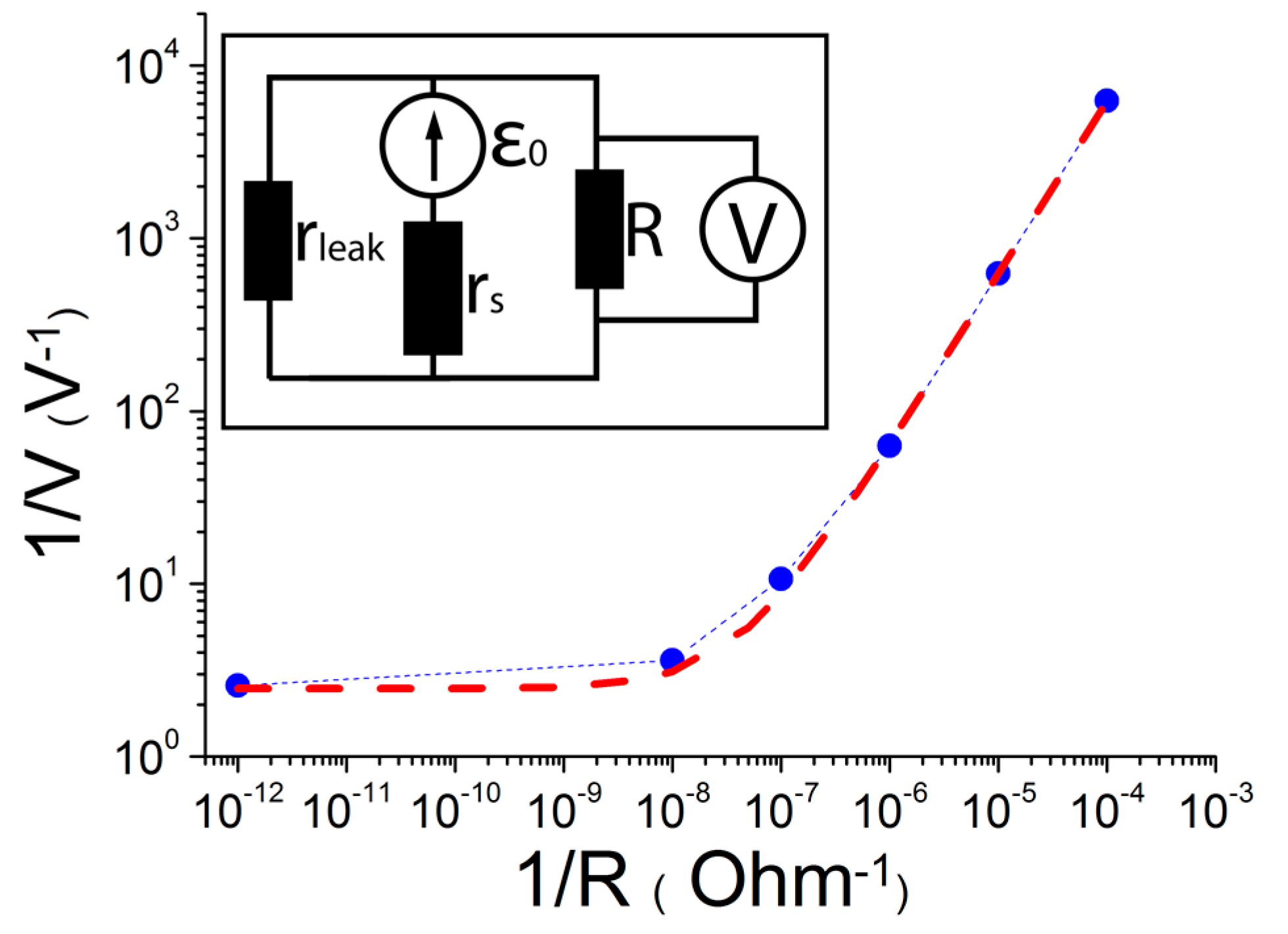
rleak values, a series of measurements of load characteristics was performed, in which the structure (measured in the previous investigation) was connected to an external resistance R, the value of which could be changed (the scheme of the circuit and the results can be found in
Figure 4).
By measuring voltage V at the external resistance, we obtained the dependence V
−1(R
−1) (see
Figure 4). To find the unknown parameters (
rs and
rleak), a linear fit was performed for the following coordinates:
From the analysis of the V−1(R−1) dependence and taking into account our previous investigation (ε0 = 1.1 V) the values of rs and rleak were derived to be 6.9 × 10⁷ and 3.9 × 10⁷ Ohm, respectively.
3.2.2. Influence of Humidity
As was described above, one of the prominent peculiarities of the structures is their reaction to water vapor. It was established that there is no spontaneous emf generation in vacuum. When water vapor is introduced into the measurement chamber and the humidity of the atmosphere surrounding the structures increases accordingly, emf is spontaneously produced, leading to a potential difference between the electrodes encasing the nc-Si film.
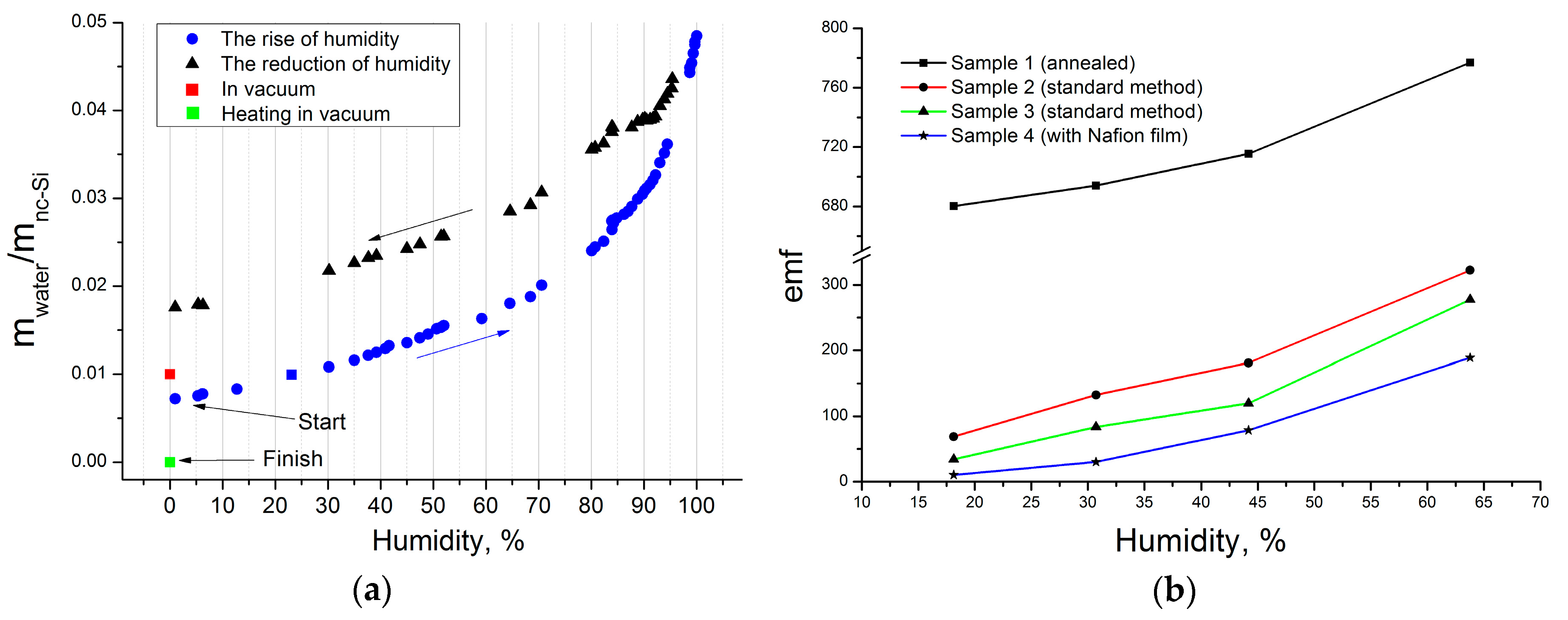
To quantify the minute amount of water absorbed by nc-Si film, a quartz microbalance based on oscillation frequency measurement (12 MHz) was used. Each value was obtained by comparing the frequency of the test sample with an empty reference sample. Humidity was increased stepwise from an argon atmosphere (see
Figure 5a). After reaching the maximum, the humidity was lowered to zero, but a considerable amount of water was caught by the structure. The final stage of our experiment was vacuum degassing (400 K, 2 h, 10
−5 Torr). The mass value reached in this process was treated as the baseline mass of the pure nc-Si film (
Figure 5a, green square), and water mass was identified as the excess. The structure was found to absorb between 1 and 5 mass % of water, depending on humidity (see
Figure 5a).
The influence of relative humidity on the emf of different samples is shown in
Figure 5b. We annealed Sample 1 before the investigation using the technique described earlier. Samples 2 and 3 were made on the same substrate, and the measurements indicate reproducibility of our method. Sample 4 contained a Nafion film. All results are subject to the same law, close to linear. The significantly higher emf value of Sample 1 is evidence of the positive effect of annealing.
As was mentioned, there is no spontaneous emf generation in vacuum. Sample 1 is not an exception to this rule, and the high value of emf at humidity close to 16% is due to the higher density of the sample after annealing, and its greater ability to hold water molecules. After keeping Sample 1 in a desiccator for several weeks, the emf value dropped to zero.
The nature of the emf dependence on humidity for Nafion structure (Sample 4) allows us to state that the process of emergence of electrical potentials at the electrodes of the studied structure is connected with ion transport.
3.3. Comparative Analysis of Current-Voltage (I-V) Characteristics
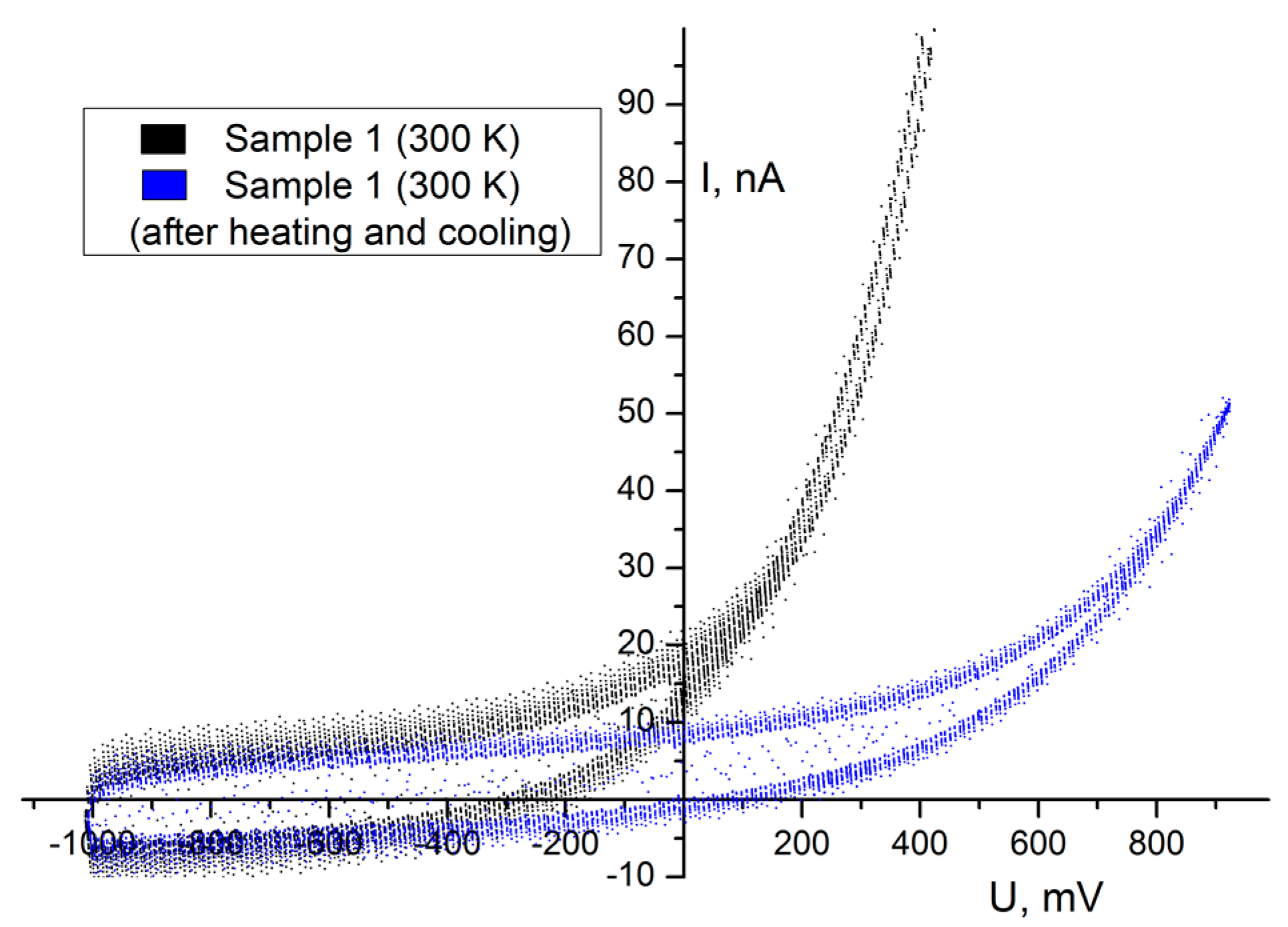
Investigation of volt-ampere characteristics (VACs) allowed us to find an influence of humidity and temperature on emf and discharge current value. VACs of all samples were asymmetrical (
Figure 6), which allows one to ascertain the existence of electrochemical processes in the structure. Oxidation processes on the top and reduction processes on the bottom electrodes lead to positive current values. In fact, this corresponds to the fast discharge of a galvanic structure. Negative current values correspond to reverse processes.
It can be clearly seen in
Figure 6 (black curve) that initial VACs at ambient conditions possessed significantly higher discharge current values (at the same voltage) and emf than after heating the sample to 340 K and recooling to 300 K (see
Figure 6, blue curve). Recooling the sample didn’t allow us to get initial emf and discharge current values. This feature shows that the influence of humidity is very large.
The possibility of porous silicon oxidation in pure water (pH ~ 7) coupled with molecular hydrogen formation has been demonstrated before [
25], the effectiveness of the process is associated with the very high specific surface area of nanocrystalline silicon. We would also like to note Ref. [
26], which is related to hydrogen generation with the use of particles obtained via laser-induced silane pyrolysis. The particles studied had a mean size similar to that of those considered in this paper. It was shown that the etching of nc-Si in water is isotropic and occurs at a rate of 3 × 10
−4 μm/s at pH = 7. Accordingly, we consider the following reactions of nc-Si oxidation (the potential values [
27] are given for the same reactions in aqueous solutions, and are present as a reference):
A supply of water molecules is needed in each process, and we suggest that sample drying leads to a decrease of current values because of a decline in reaction rate. It is also important that the second reaction shows a tendency to saturation [
25,
28]. That is the result of formation of a SiO
2 layer on the silicon surface that inhibits contact between silicon lattice and water molecules. This effect is not prominent for nc-Si because of the high specific surface area of the material.
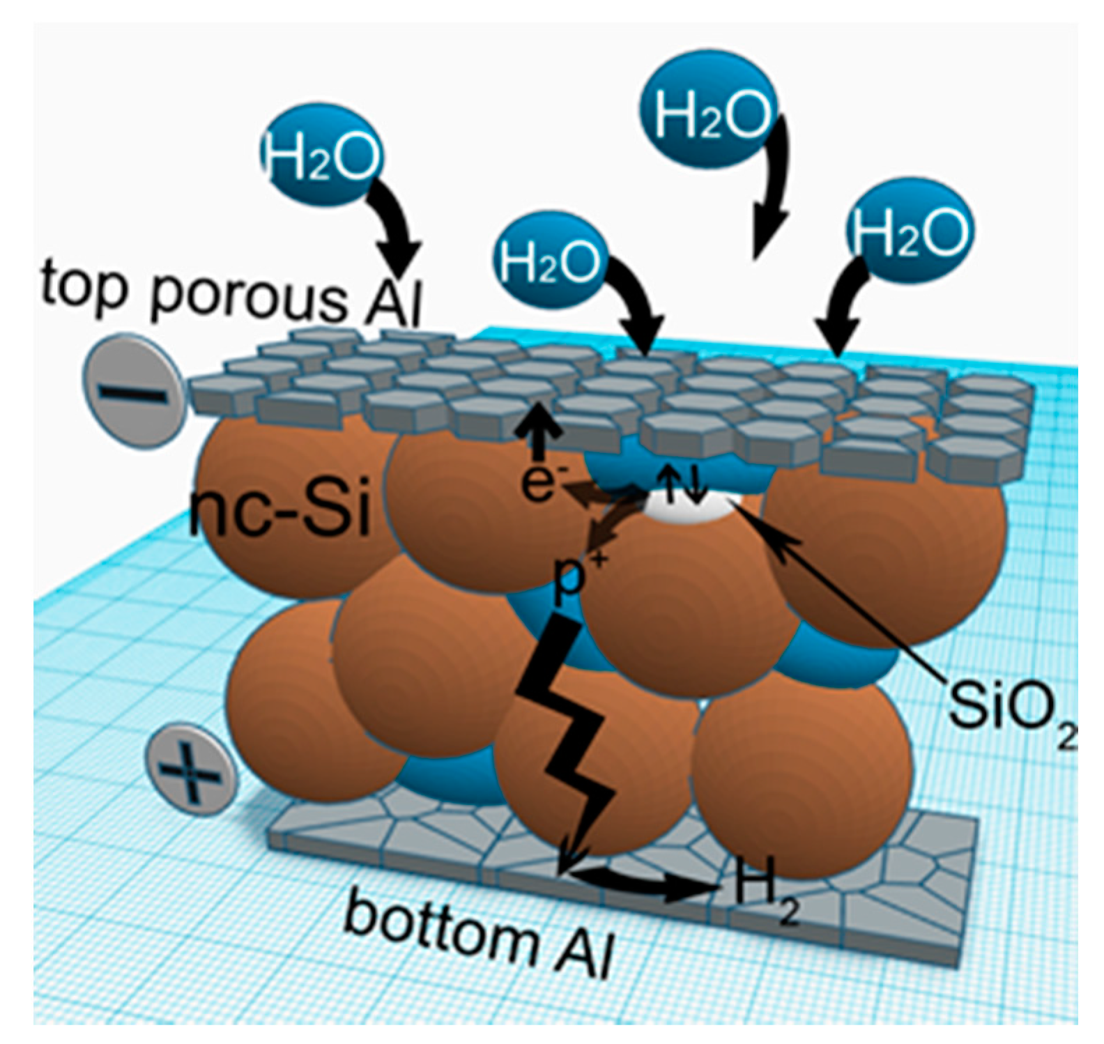
The emf generation in Al/nc-Si/Al structures is initiated by the diffusion of water vapor through the porous contact, leading to oxidation of nc-Si. The electrons injected in the conduction band of nc-Si as a result of oxidation, reach the top contact by hopping, and create a negative charge on it, whereas protons diffuse to the bottom contact, where they are reduced to hydrogen (see
Figure 7):
Should the electrodes be almost symmetric (e.g., interdigitated structures, where electrodes are deposited at the same time), electrode potentials would be identical and emf observation would be impossible. We suggest that there is a natural aluminium oxide layer on the bottom Al electrode, which was formed before nc-Si film deposition. This layer would create a barrier between nc-Si and the bottom electrode. At the same time, the boundary between the top electrode and nc-Si doesn’t contain an aluminium oxide layer.
The aluminium-Al2O3-electrolyte contact possesses rectifying properties. Electrons move from the Al electrode to electrolyte, lead to electrochemical reactions on the Al2O3 surface, and can’t return to Al. This effect is widely used in electrolytic capacitors. Due to this feature, processes of hydrogen reduction can take place on this electrode, and significant asymmetry of the investigated structure is realized.
A significant portion of charge transport in the film happens through diffusion of H
+ ions [
19]. This is supported by studies of impedance spectra in our previous work [
29] and the possibility of emf generation in Nafion structures. Proton motion can occur by transferring along hydrogen bond grids, or molecules of water adsorbed between nc-Si.
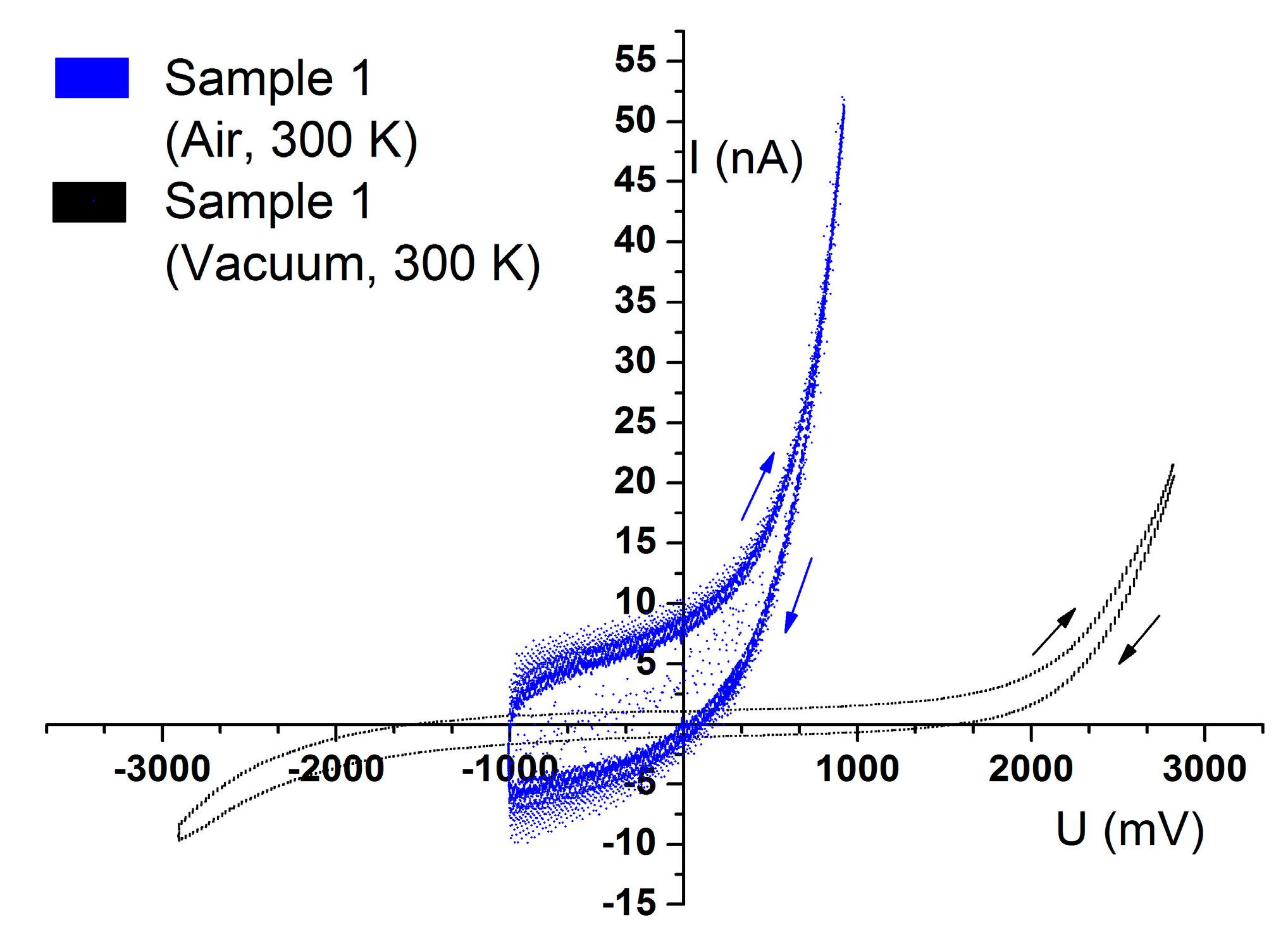
Our final investigation of humidity influence was vacuum measurement (~10
−2 Torr). It was established that the emf value tends to zero (
Figure 8).
4. Conclusions
It was shown for the first time that a thin film Al/nc-Si/Al structure with a porous top contact may spontaneously generate emf upon interaction with water vapor in the surrounding atmosphere. The most important fact is that such structures are spontaneously formed by a self-assembly process during layer coating. The high porosity of nc-Si film isn’t suitable for efficient charge transfer. Therefore, annealing is needed prior to top electrode deposition.
The value of emf increases with the temperature of the structure. Upon analysis of the activational dependences of the emf, it was established that electrical charge leak processes significantly affect the value of emf. We suggest that water reacts with the nc-Si surface, resulting in the formation of an oxygen silicon compound. It is this process that is the origin of energy generation in the structures. Water is thus necessary for the chemical reactions and proton conductivity that lead to emf generation. The role of proton conductivity was confirmed by separation of the structure by a Nafion membrane.
It is important to mention that the possibility of emf observation is related to the asymmetry of the two aluminium electrodes. There is an oxide layer between the bottom aluminium electrode and the nc-Si film; on the other hand, there is no such layer between the top electrode and the nc-Si. This feature leads to the impossibility of electron transfer to the bottom electrode, but does not prevent hydrogen reduction on it.
Due to the simplicity of the thin structures obtained, such a source may be introduced into electronic paper and employed in the next generation of smart cards. Moreover, it is not necessary to use a liquid electrolyte, and structures may easily be manufactured directly on the surface of silicon chips.

