1. Introduction
Security has become a major concern for integrated circuits (ICs) because of globalization and outsourced offshore production. Throughout the lifecycle of the IC, the chip could be under attack from overproduction during the manufacturing stage to unauthorized recycling after customer disposition [
1]. Furthermore, a manufacturer could make extra chips by cloning during the manufacturing stage after obtaining the design by reverse engineering [
2,
3]. State of the art IC reverse engineering is so advanced that the chips could be reverse engineered within a few weeks. There are dedicated companies that do reverse engineering of new industrial chips. Therefore, a scheme is required to prevent the production of illegal cloned chips by reverse engineering.
Hardware obfuscation is an approach to prevent IC piracy and reverse engineering. Hardware obfuscation could be categorized into two types: Logic or functional locking and camouflage. The main idea behind logical locking obfuscation is that part of the design is replaced with a configurable module at the design stage. If the module is not activated by the designer, the chip will not function properly [
4,
5,
6,
7]. During the post-fabrication activation process in a trusted design house, the chips can be activated by unlocking the obfuscated function with a secret key that may be burned into on-chip fuses. Those unlocked chips can then be sold to the open market. The stored key can not be recovered without direct access to the on-chip fuses such as with probing attacks. Therefore, an attacker can not reverse engineer the design because of the obfuscation, and the chip can not be overproduced without knowledge of the key. Furthermore, layout level techniques such as cell camouflage [
8] could be used as hardware obfuscation and dummy contacts are used to protect against attackers. The layout of standard cells with different functionalities is made to appear identical in the camouflage technique. Camouflaging can make it more difficult to identify camouflaged gates with automated image tools. In this paper, we have focused on logic locking-based hardware obfuscation.
Several conceptually new and interesting approaches have been proposed to introduce forms of obfuscation or logic locking to prevent reverse engineering and piracy. For example, additional exclusive OR (XOR) gates can be inserted in combinational designs with configurable bits that need to set correctly to activate the chips [
6]. Dummy states can be inserted into finite state machines in sequential designs, requiring certain sequences of inputs to be applied for the circuits to function correctly [
9]. Scrambling the interconnection network in a permutation-based technique will cause the circuit to only work with a correct key which will configure the interconnection network [
10]. Other work has hidden parts of the circuit in a configurable lookup table (LUT) [
11]. With those obfuscation methods, the effort for an attacker to find the correct key will become computationally infeasible [
12]. The assumption made with these methods is that there is no direct access to the key content [
6,
13].
A problem with many of these approaches is that the key is not unique across all instances of the chip. Thus, if an attacker is able to retrieve the key by some method, it can unlock all chips and effectively overproduce the chips. Recently, physically unclonable functions (PUFs) have been used as a way to provide unique keys for obfuscation [
14,
15,
16]. PUFs are inherent circuit primitives that extract randomness from the physical characteristics of a system at the manufacturing stage [
17,
18] by applying input challenges and observing random output responses. PUFs are easy and simple to implement but their random nature ideally makes its behavior hard to predict and model for an attacker.
Some of these PUF-based obfuscation approaches require a full characterization of the PUF input-output response, thereby necessitating a relatively small output space for the PUF. Such PUFs are called weak PUFs. An untrusted foundry could do the same characterization and could store the challenge-response pairs (CRP) for all chips before sending them to the design house. If a key leaked from an activated chip, the untrusted foundry could recover the entire design with the leaked key and, using its PUF characterizations, be able to unlock all chips whether authorized or not.
Strong PUFs, on the other hand, have a very large input/output space, making characterization impractical and thus much more secure. However, at the same time, it makes some PUF-based obfuscations approaches infeasible. It would be ideal to have an obfuscation scheme that can take advantage of these strong PUFs to improve the security of the approach. In this paper, we have proposed using a strong PUF with a subset of bits used to generate a key that can unlock a locked circuit. A mathematical probability model is developed which determines the feasibility of the PUF key.
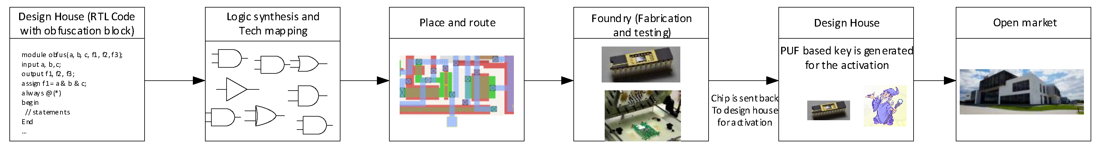
In
Figure 1, the design and fabrication flow is shown for a prevention method of piracy and overproduction of chips using a PUF-based method. The designer uses logic synthesis, technology mapping, and place and route tools to produce a graphic database system II (GDSII) file that can be sent to the fabrication facility. Fabricated chips will be manufactured and tested at the foundry and will be sent back to the design house for activation. The design house will activate the chip using the PUF-based key and will send to the market for sale.
The rest of this paper is organized as follows. First, we describe prior related work. Second, we provide in detail a description of the proposed PUF-based hardware obfuscation method. Next, we describe attack analysis for our proposed method. After that we analyze our technique based on performance analysis. And finally, we evaluate our technique on different ISCAS 85 benchmarks.
2. Prior PUF-Based Obfuscation Approaches
A PUF is an unclonable hardware function based on process variation during fabrication. A PUF has a set of challenge response pairs (CRP) which are the input and output respectively. The CRPs represent a random function which is unique to each chip. It is impossible to make identical PUFs with the same CRPs [
18]. PUFs have been used in different applications including secret key generation, device authentication, and anti-counterfeiting [
19]. Below, we describe prior weak PUF and strong PUF-based approaches to prevent reverse engineering and piracy.
Wendt et al. [
15] created a unique key per chip using a weak PUF. A part of the circuit’s functionality was replaced with a PUF and a lookup table (LUT). The functionality of the PUF and the LUT together was equivalent to the original circuit functionality. The content of the LUT for each chip was determined by the designer after obtaining the PUF’s CRPs. Thus, the LUT behaved as a key that would be uniquely configured by the designer in the post-fabrication activation process. A problem with this method was that an untrusted manufacturer could have access to the PUF during the fabrication process. The manufacturer could obtain the CRPs of the weak PUF easily and store those results. If the attacker could find a leaked LUT key of an activated chip in the aftermarket, in combination with the previously stored PUF functionality of the leaked chip, it was trivial to then determine LUT keys for any device.
Khalegi et al. [
14] used a similar approach but with a strong PUF with a large CRP space. In order to make the use of a strong PUF feasible, the designer’s characterization of the PUF was limited to just a subset of the input set. For example, if the input of the PUF is
p bits long, then only
n bits were used for characterization by the designer, where
. However, an attacker would have to still characterize the entire
p-bit input PUF. An obfuscator circuit was used to select the
n input bits. The added complexity of an obfuscator circuit and selection bits added to the overhead. Moreover, the approach does not scale well because as
n grows, the complexity of the LUT grows exponentially. Thus, one can not obfuscate large circuits, but only small subsections of the circuit. Furthermore, another limitation of this approach is that it does not account for collision of PUF outputs—i.e., with small
n it is likely that different inputs could produce colliding PUF outputs, which means it would be impossible to realize a LUT that will satisfy the design functionality. To overcome those limitations, we similarly propose a hardware obfuscation method that does not require the full characterization of a strong PUF and has significantly less overhead.
Alkabani et al. [
20] used a strong PUF (or RUB as it is called in the paper) to generate bits that could then be transformed into a code to unlock the FSM-based locking scheme. Specifically, a specific input external key was applied as a challenge to the PUF response and XOR’d with a separate external key to generate the appropriate internal key that unlocks the FSM. Note that we refer to “internal key” as the internal bits that unlock the locked circuit, while “external key” is the set of bits that are applied externally by a user or from stored memory. Our approach also uses a strong PUF to generate responses based on an input challenge. However, the distinction is that we allow the PUF response to directly create the internal key (or sub-key). In other words, we apply multiple challenges where each response forms part of the internal key. The external key is the set of challenges that are used to create the internal key. This simplifies the circuitry since the PUF output does not need to be as large as the internal key and moreover removes the need for any XOR circuitry.
3. Strong PUF-Based Key Generation
The main idea of the proposed methodology is to eliminate the use of a LUT for obfuscation and use one of the many existing key-based hardware obfuscation methods [
21]. These methods have much lower overheads than LUTs for large
n. The PUF-based obfuscation architecture is shown in
Figure 2. The key will be directly generated from a strong PUF given the appropriate challenge. The key can then be provided to any key-based obfuscation method. We assume a PUF with
p inputs and
n outputs where
. One can use an obfuscator circuit to limit the input set, but as we will show, that is not necessary for large
n. Large
n can be problematic in terms of characterization, but for our approach a full characterization is not necessary.
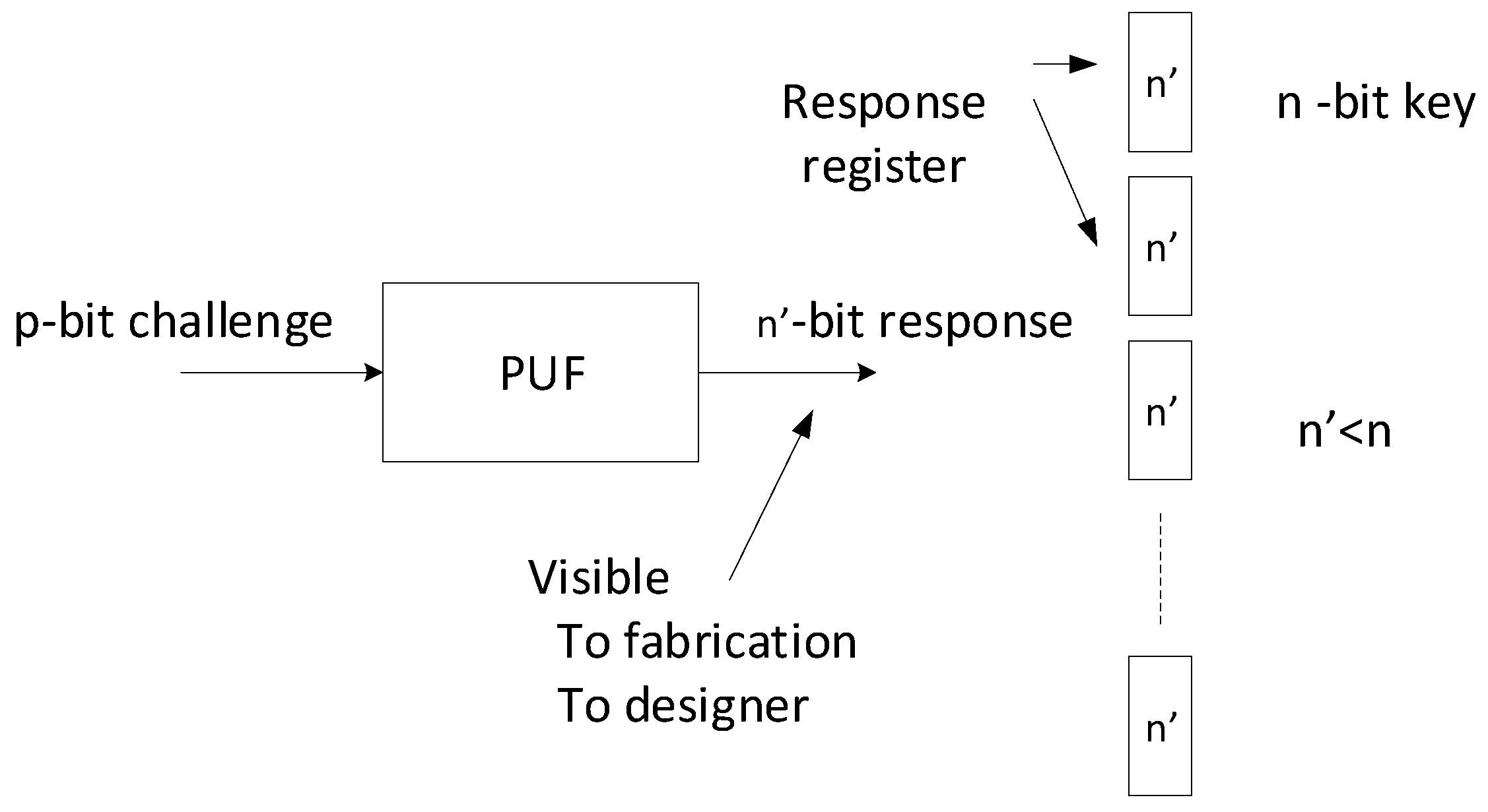
Assume that the PUF generates an
n-bit response given a
p-bit challenge. As the designer, instead of characterizing the entire
p-bit input space of the PUF, we only need to find one PUF input that matches the desired key of the locked circuit. Assuming a truly random PUF, on average, that will take
brute force tries, rather than the
challenges needed to characterize the entire PUF. As
n gets large, however, even that can become difficult. Therefore, instead of using a
n-bit PUF, we use only
bits of the PUF output, where
. In order to generate the key, we issue
challenges, where each response is stored in a
-bit sub-key register. The
S sub-keys together form the
n-bit key
K:
An attacker would need to apply S p-bit challenges in the correct order to find the right key to unlock the device—in other words they would need to guess challenges.
The flow diagram for PUF-based obfuscation is shown in
Figure 3. Our goal is to generate a specific obfuscation key (
K) from a set of challenge bits (
C) that is unique to a specific chip as shown in
Figure 3a. Internally, the key generation block consists of a PUF and sub-key registers as described earlier (
Figure 3b). The sub-keys which will be used for the final key which will be configured by the designer during the post-fabrication activation shown in
Figure 3c. To configure the sub-keys, the designer obtains the CRPs from the PUF during the activation process using the characterization channels
Figure 3c. After characterization, the designer should remove the channels (
Figure 3d) so that the PUF cannot be probed after market. Techniques to remove the characterization channels include laser burning the accessing wires and burning the supporting fuses, amongst other approaches.
3.1. Challenge Selection Process
Before a chip can be activated, the designer must select the challenges required to generate the PUF responses/sub-keys that can be combined to create the obfuscation key. As mentioned above, we have divided the
n-bit key into
S -bit sub-keys as shown in more detail in
Figure 4. The sub-keys will be visible to the designer and manufacturer but not to the end user. In order to find a challenge that generates a particular sub-key, we need to try, on average,
challenges. Since we have to find
S sub-keys, we need to find
S challenges (assuming no repetitions in the sub-keys).
How many challenges do we need to try to find these
S sub-keys? Or, put another way, given that we will attempt
N challenges, what is the probability we find the
S sub-keys? The
N p-bit challenges generate
N -bit responses. Assume that
of the responses do not contain any of the required
S sub-keys, or in other words,
i responses contain all of the
S sub-keys and only the
S sub-keys (with repetition). There are
possible positions for those
i responses. Those
i responses can be partitioned into
S buckets in
ways, where
is the Stirling number of the second kind:
The remaining
responses have
possibilities. Given that there are in total
possible responses to the
N challenges, we can put it all together to arrive at the probability that we find the
S sub-keys:
Using a similar analysis to the coupon collector problem, the expected value for
N can be calculated as:
For example, when , , and , the probability that you will get all 16 sub-keys is 0.999997. The expected number of challenges we need to get the 16 sub-keys is 865. When and , the expected number of challenges to find the 16 sub-keys we need is 221,559—not an unreasonable number. As grows, the expected value grows exponentially. For and , the expected value is . At 10 ns per challenge, it would take roughly two minutes to find the required sub-keys. A larger provides security against attackers who have advanced probing capabilities and have visibility to the PUF responses and can thus limit their challenge tries to rather than for those that don’t. However, if that is not a concern, a smaller is more practical.
3.2. Chip Activation
Chip activation could be accomplished in a number of ways. In one approach, once the challenges have been selected by the designer, they can be programmed into one-time-programmable ROMs and fused in permanently. This allows the designer to control the activation process. Fuses, however, can be reverse engineered, so care must be taken to have these sub-keys programmed in such a way that cannot be recovered. Alternatively, end-user customers can activate the chip directly with activation challenges provided by the designer. These challenges would be unique to each chip, but since the challenges are not permanently programmed into the chip, they would need to be reapplied on every powerup. This approach allows users to effectively disable a chip until some trusted hardware or software has enabled the chip with the appropriate challenges. There may be scenarios where chips are shipped directly from manufacturer to customer. In this case, the PUF characterization channel will need to be left open. The customer could then apply several challenges and get the associated responses for the key. These could be sent to the designer, who can select the specific challenges that will generate the activation key. After activation, an automated mechanism can disable the characterization channel so that those channels can not be used in future. This approach opens up more attack possibilities—for example, end-users can now use machine learning attacks to characterize the PUF, and with known “good” responses, they can possibly recover the key. Therefore, this last activation method should be used only with trusted customers.
6. Evaluation
We have evaluated the effectiveness of our proposed technique by implementing it on an fiweld programmable gate arrays (FPGA) and calculating the hardware overhead. Note that in this paper, we do not report the overhead of the PUF implementation on the FPGA. The overhead of PUF implementations on FPGAs are well reported [
24,
25,
26], and our approach does not depend on any specific strong PUF implementation. Furthermore, if a PUF is already used in a circuit for hardware security/authentication, the same PUF could be used for obfuscation key generation as well. We have performed the experiments on a number of ISCAS85-based obfuscation benchmarks [
21]. Again, our approach will work with any key-based obfuscation method. For the purposes of these experiments, we have used logic cone size-based obfuscation [
27] along with the key generated from the strong PUF. In the logic cone size-based obfuscation method, the locked logic is placed in the largest logic cones so that it can impact more signals. A weighted normalized metric for all gates is measured and compared to find the position of the largest logic cone in the module under consideration. Both the fanin and fanout cones of a gate are considered as the metric. Therefore, gates with a higher value of this metric will have higher fanin and fanout and will be chosen as a locking gate in the inputs.
The benchmarks have been synthesized using Xilinx Vivado.
Table 1 shows the characteristics of the ISCAS85 benchmarks under evaluation and the FPGA utilization as reported by Vivado. We have illustrated comprehensive area overhead evaluations on the ISCAS85 benchmarks suite in
Table 2. The benchmark circuit name is shown in the first column. The second column demonstrates the different key sizes used for obfuscation. Columns 3 and 4 show the area overhead in terms of LUTs due to obfuscation and the overhead that key generation adds to obfuscation after implementation on FPGA. Overheads in percentages have been shown in the last two columns.
Figure 5 shows the area overhead for the key generation compared to the base obfuscation method [
27] with different key sizes and benchmark circuits. It is noted that the area overhead for the key generation is typically less than 4% for different benchmarks and key sizes.
Depending on the internal design and architecture, a PUF can take multiple clock cycles to evaluate the response. In
Table 3, we show the impact of the evaluation time on the overhead. As the clock cycles increase, the number of registers increase logarithmically primarily to keep timing state. We also see the difference in utilization for a 16-bit PUF (
) compared to a 32-bit PUF (
). Consider the 1-clock cycle 64-bit key case. For a 16-bit PUF, we need 67 registers total—64 registers for the key, two registers to keep track of the four sub-keys, and one more register for control logic state. As we increase
, the key generation cost goes down slightly because
S goes down. However, it comes at the expense of a larger PUF and more effort to find the challenges (Equation (
4)).


