Article

SCANN: Side Channel Analysis of Spiking Neural Networks

1
School of Electrical Engineering and Computer Science, The Pennsylvania State University, State College, PA 16801, USA
2
IBM Corporation, Hopewell Junction, NY 12533, USA
3
Ampere Computing, Portland, OR 97209, USA
*
Author to whom correspondence should be addressed.
Cryptography 2023, 7(2), 17; https://doi.org/10.3390/cryptography7020017
Submission received: 19 January 2023 / Revised: 19 March 2023 / Accepted: 21 March 2023 / Published: 27 March 2023
(This article belongs to the Special Issue Feature Papers in Hardware Security II)

Abstract

:
Spiking neural networks (SNNs) are quickly gaining traction as a viable alternative to deep neural networks (DNNs). Compared to DNNs, SNNs are computationally more powerful and energy efficient. The design metrics (synaptic weights, membrane threshold, etc.) chosen for such SNN architectures are often proprietary and constitute confidential intellectual property (IP). Our study indicates that SNN architectures implemented using conventional analog neurons are susceptible to side channel attack (SCA). Unlike the conventional SCAs that are aimed to leak private keys from cryptographic implementations, SCANN ( SCA ̲ of spiking n ̲ eural n ̲ etworks) can reveal the sensitive IP implemented within the SNN through the power side channel. We demonstrate eight unique SCANN attacks by taking a common analog neuron (axon hillock neuron) as the test case. We chose this particular model since it is biologically plausible and is hence a good fit for SNNs. Simulation results indicate that different synaptic weights, neurons/layer, neuron membrane thresholds, and neuron capacitor sizes (which are the building blocks of SNN) yield distinct power and spike timing signatures, making them vulnerable to SCA. We show that an adversary can use templates (using foundry-calibrated simulations or fabricating known design parameters in test chips) and analysis to identify the specifications of the implemented SNN.

1. Introduction

Artificial neural networks (ANNs or NNs), which are inspired by brain functionality, are composed of layers of neurons interlinked by synapses and can be used to approximate any computable function. The use of neural networks in safety-critical domains, such as autonomous driving [1], healthcare [2], internet of things [3] and security [4], necessitates an examination of their security vulnerabilities and risks. In real-world applications, attacking a neural network can result in undesirable inferences that can compromise safety (e.g., reduced accuracy or confidence in road sign identification during autonomous driving). These attacks can be launched during the training, manufacturing, or final application stages.
Spiking neural networks (SNNs) [5], the third generation of neural networks, are emerging as an alternative to deep neural networks (DNNs) since they are biologically plausible, computationally powerful [6], and energy efficient [7,8,9]. The majority of past work in SNN security focuses on evaluating the robustness of SNNs when exposed to adversarial input noise. The vulnerabilities/attacks of SNNs under a white-box scenario, e.g., sensitivity to adversarial examples and a robust training mechanism for defense is proposed in [10]. A white-box fault injection attack is proposed [11] for SNNs by employing adversarial input noise. In [12], a black-box approach is presented to generate adversarial input instances to induce misprediction in SNNs. In [13,14], power-based voltage fault injection (VFI) attacks are demonstrated against analog neurons to cause degradation in SNN accuracy.
The primary motivation behind SCANN ( SCA ̲ of spiking n ̲ eural n ̲ etworks) is due to the vulnerability of SNN to side channel attacks (SCAs). An SCA can extract sensitive information through a variety of methods, such as power [15,16], timing [17,18], and electromagnetic emanations [19,20]. Power and timing side channel attacks are the most predominant. Reverse engineering (RE) attacks using SCA have already been demonstrated for ANNs [21] via the extraction of sensitive metrics, such as activation functions, synaptic weights, neurons/layer and number of output classes. However, very limited research exists on the security of SNNs against SCA-based RE. In [22], the authors identified timing/power side-channel vulnerabilities in an SNN system. However, the work is restricted to only identifying the spiking activity and number of neurons implemented. Furthermore, the authors analyzed only a FPGA-based digital implementation of an SNN while not considering analog implementations for simplicity. Sensitive SNN metrics, such as the neuron’s synaptic weights or neuron’s membrane threshold, require significant training, design effort, time, and financial resources. This provides strong motivation to analyze the power/timing side-channel leakage of SNNs and identify the multiple confidential design parameters that an adversary can extract from the leakage.
Figure 1 depicts the proposed threat model. Our studies indicate that the power profile of SNN has distinct markers that can be utilized to extract sensitive design parameters. The SNN power profile can be accessible to the adversary (especially for edge devices, where physical possession of the device by the adversary is possible) since the SNN draws its current from an external power source (i.e., V D D pin). The threat model in this paper is adversarial monitoring of the power drawn by using simple probes at the V D D input to steal design/training metrics of the SNN system. This can be achieved by analyzing the extracted power profiles to infer critical features, such as the timing of spike markers, average current, peak current, or min current during SNN operation (as shown in Figure 1). These features are found to be unique for different training metrics and design choices. Note that the considered power SCA on SNN is different than conventional power SCA on cryptographic primitives, where the objective is to break the key and subsequently steal the plaintext data sent over the network.
Multiple attack scenarios are presented in this work: (i) Insider adversary (e.g., adversary in cloud computing farm who can place a probe in the power port and collect the traces). (ii) Physical possession/attack by the user—malicious insertion of power logger and transmitter to devices, such as PCs, gaming consoles, power adapters during use by an adversary who has physical access to the device (e.g., public computer). (iii) Academic researchers/white hat adversaries who aim to investigate security vulnerabilities of systems to develop countermeasures can also conduct this experiment.
In summary, the following contributions are made in this work. We (a) present detailed analysis of the power side channel of an analog neuron model, axon hillock neuron, (b) identify unique markers in the SNN power profile to extract spiking activity and average power, (c) present eight attack models to analyze metrics in the power profile to reverse engineer and derive confidential design parameters of SNN, and (d) present discussions on process variation analysis and defenses.
The rest of the paper is organized as follows: Section 2 presents the background on SNNs and neuron design and simulation setup, Section 3 and Section 4 present an analysis of the timing and power side-channel attacks on SNN, Section 5 presents the discussion, process variation analysis and defenses, and finally, Section 6 draws the conclusion.

2. Background

In this section, we present the overview of SNN and neuron design [23] that are used in this paper.

2.1. Overview of Spiking Neural Network

SNNs are composed of layers of spiking neurons that are interconnected together by synaptic weights (Figure 1). The neurons between adjacent layers exchange information in the form of spike trains. The timing of the spikes and the strength of the synaptic weights between neurons are critical parameters in SNN operation. Each neuron includes a membrane, whose potential increases when the neuron receives an input spike. The neuron fires an output spike when this membrane potential crosses a pre-determined threshold. Various neuron models, such as, I&F, Hodgkin–Huxley, and spike response, exist with different membrane and spike-generation operations. In this work, we implemented a flavor of the I&F neuron to showcase the power-based attacks. Leaky integrate and fire (LIF) neuron models are simple, computationally effective, and are the most widely used spiking neuron models. The axon hillock (AH) neuron model described in the paper is used as a representative LIF neuron in our SNN to depict the effectiveness of the proposed SCA. The AH is an early implementation of an artificial LIF neuron circuit. It has extensively been used to generate spikes in SNN implementations [23,24,25,26,27] forming a basis for contemporary LIF designs. In this work, we implement, simulate, and analyze all neuron models on HSPICE using PTM 65nm technology.

2.2. Axon Hillock Spiking Neuron Design and Implementation

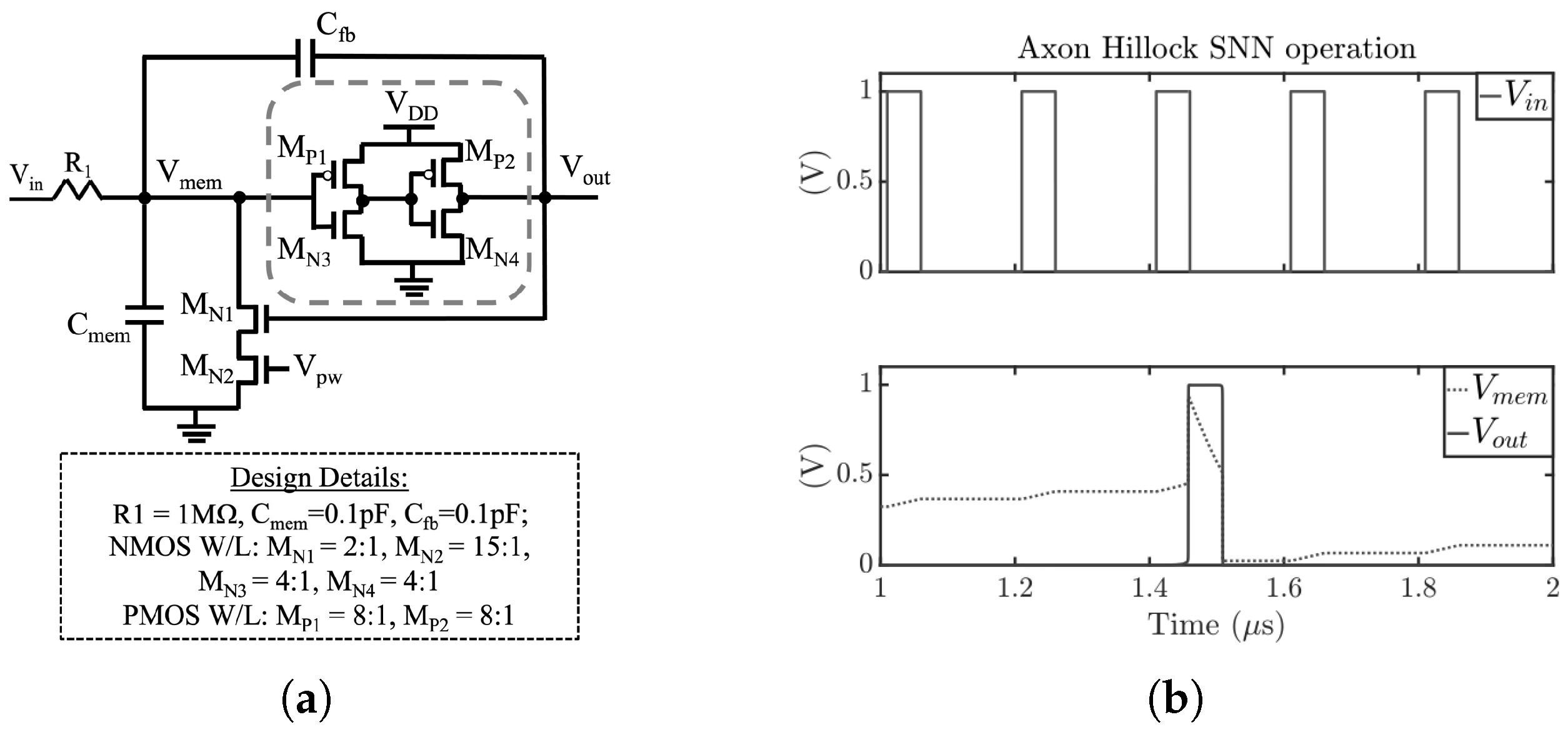
The axon hillock circuit [28] (Figure 2a) consists of an amplifier block implemented using two inverters in series (shown in dotted gray box). The neuron receives its input spikes through a synapse (1 M Ω resistor). The input voltage ( V i n ) is integrated at the neuron membrane capacitance ( C m e m ), and the analog membrane voltage ( V m e m ) rises linearly until it crosses the amplifier’s threshold. Once it reaches this point, the output ( V o u t ) switches from ‘0’ to V D D . This V o u t is fed back into a reset transistor ( M N 1 ) and activates a positive feedback through the capacitor divider ( C f b ). Another transistor ( M N 2 ), controlled by V p w determines the reset current. If reset voltage > V i n , C m e m is discharged until it falls to the amplifier’s threshold. This causes V o u t to switch from V D D to ‘0’. The output remains ‘0’ until the entire cycle repeats. Figure 2b depicts the expected results of V m e m and V o u t .
In this paper, the value of membrane capacitance ( C m e m ) and the feedback capacitance ( C f b ) of 0.1 pF are used. For experimental purposes, the input voltage spikes with an amplitude of 1 V, a spike width of 50 ns, and a spike rate of 5 MHz are generated through the voltage source ( V i n ). The V D D of the design is set to 1 V. Figure 2b shows the simulation results of the input current spikes ( I i n ) and the corresponding membrane and the output voltage ( V o u t ).

2.3. Simulation Setup

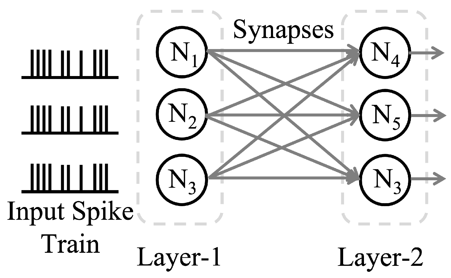
The axon hillock neuron model described in Section 2.2 is used as a representative neuron for our SNN to depict the effectiveness of the proposed SCA. While SNN architectures may widely vary on the number of neurons per layer, we chose a 2-layer 3 × 3 architecture (Figure 3) as our baseline representative example since this is simpler to simulate and to conduct further analysis. For our experimental purposes, we considered the SNN implementation as an isolated system and not as a part of an SoC.

2.4. SNN Side-Channel Analysis

To design the reverse engineering attack against the presented neurons, we first investigate their power signature. The SNN system’s operation indicates that the consumed power depends on its spiking activity. Here, we present the characteristics of the power profile observed for the SNNs under attack presented in Section 2.3.
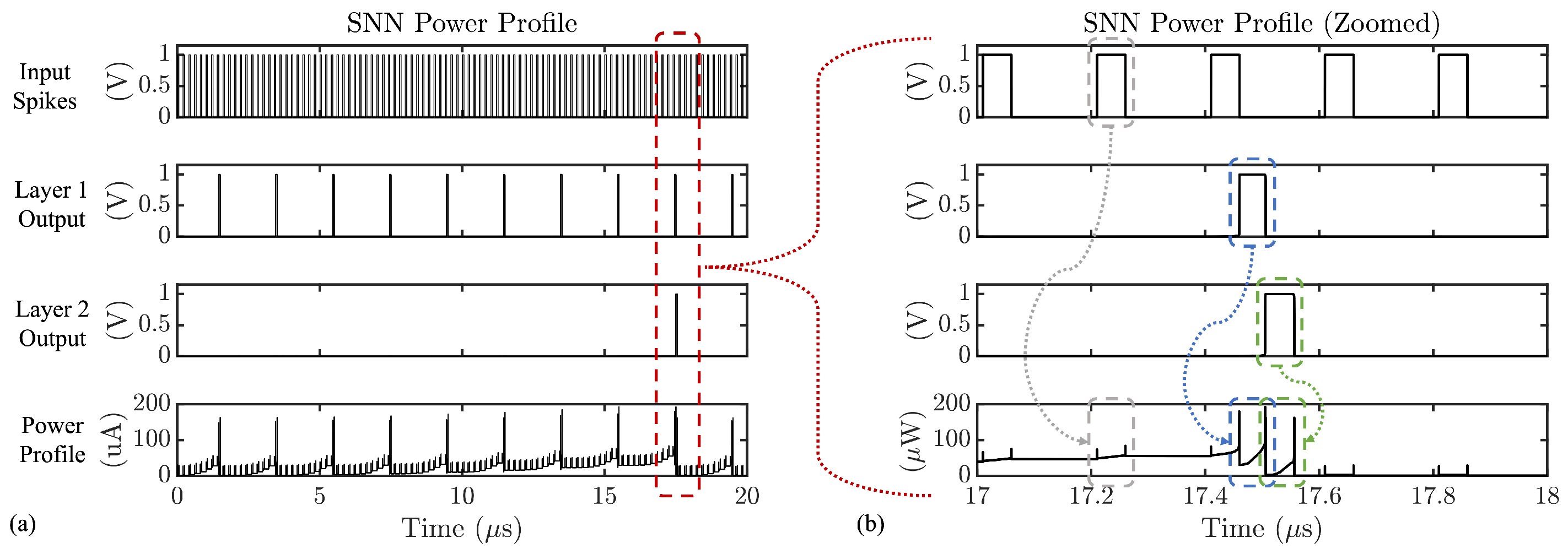
We simulate the 2-layer 3 × 3 SNN architecture to observe its power profile. There are three different types of spikes that occur during SNN operation. They are (i) input spikes, (ii) Layer-1 spikes, and (iii) Layer-2 spikes. Figure 4a shows the three types of spiking activity and the observed power profile. The simulation period marked by the red box, where all three types of spikes occur, is zoomed in and shown in Figure 4b. Each voltage spike causes a pair of current spikes in the power profile: one each during the rising edge and falling edge of the voltage spike. In Figure 4b, each kind of voltage spike and its corresponding pair of current profile spikes are marked in colored boxes: grey (input spike), blue (Layer-1 spike), and green (Layer-2 spike). The results indicate that the occurrence of voltage spikes causes a unique marker in the SNN power profile depending on its origin. Figure 5 depicts three unique power profile markers that indicate three spiking activity conditions of the SNN: (i) Input spike only: when only the input voltage spikes occur, we observe a pair of short power spikes; (ii) input + Layer-1 spikes: when an input spike causes a neuron in Layer 1 to spike, we observe a short pair of power spikes, caused by the input, followed by a tall pair of power spikes, caused by Layer-1 output spike; (iii) input + Layer-1 + Layer-2 spikes: when an input spike causes a Layer-1 spike, which in turn causes a Layer-2 spike, we observe one short, and two tall pair of power spikes.

3. SCANN Attacks Using Timing Side Channel

In Section 2.4, the effect of various design parameters on SNN power profile is analyzed. Here, we describe techniques to leverage the power profile to extract the time-to-spike (timing side channel) and reverse engineer the SNN design parameters.

3.1. SCANN 1: Effect of Synaptic Weights

A 3 × 3 2-layer SNN (shown in Figure 3) is used to analyze the effect of synaptic weights on the SNN power profile. In this example, we analyze the spiking activity of neuron N 4 in Layer-2. The synaptic weights of all synapses from Layer-1 connecting to neuron N 4 are changed. Figure 6a shows the N 4 spiking activity for two cases of input synaptic weights, where all synapses to N 4 are (i) 1 M Ω , and (ii) 2 M Ω . Figure 6a also depicts the power profiles of these two cases that accurately reveal the unique markers that indicate when N 4 (a layer-2 neuron) spikes. It is noted that a neuron’s time-to-spike increases as the synaptic weights to it increases. This is due to the decrease in the amount of current that is integrated over the neuron’s membrane for each spike as the synaptic weight increases. As a result, it takes longer to charge the neuron to its threshold.
The SNN power profile and unique markers can be leveraged to determine the time-to-spike value of a neuron and ultimately the synaptic weights to it. Figure 6b depicts the change in the N 4 time-to-spike for different synaptic weights and for different numbers of N 4 input synapses modified. Figure 6c depicts the spiking rate under different synaptic weights in a 50 μ s sampling window. It is seen that the spiking rate decreases as the synaptic strengths increase.

3.2. SCANN 2: Effect of Neuron Membrane Threshold

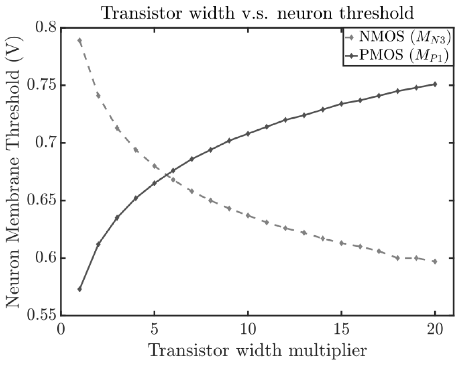
The membrane threshold of the axon hillock neuron, described in Section 2.2, is determined by the first inverter in its amplifier block. The sizing of the inverter’s PMOS ( M P 1 ) and NMOS ( M N 3 ) transistors determines the neuron’s threshold voltage ( V t h ). In order to vary V t h , the PMOS ( M P 1 ) width is varied from 1× to 20×. Figure 7 shows the effect of the M P 1 width on the neuron’s membrane threshold. This PMOS width variation is leveraged to vary the membrane threshold of all the neurons in the SNN from 0.57 V to 0.75 V. Note that the NMOS width of transistor M N 3 may also be varied to achieve a similar variation in neuron V t h as shown in Figure 7. Figure 8a shows the power profile for three specific V t h cases. The unique Layer-2 spiking markers (boxed in red) depict that the time-to-spike for a neuron in Layer-2 increases as V t h increases. This is due to the fact that the number of spikes required to trigger the neuron increases with a higher threshold. Therefore, for the same input, the SNN spiking rate decreases for a fixed sampling window. Figure 8b shows the increase in time to spike as the V t h is increased. Figure 8c shows the change in Layer-2’s output spike as V t h is increased.

3.3. SCANN 3: Effect of Number of Neurons

The baseline SNN (shown in Figure 9a) is a 3 × 3 network with 3 neurons per layer. The number of neurons per layer is varied from 1 to 10 and the corresponding power profiles are analyzed. Figure 9b shows the unique markers (boxed in red) that reveal Layer-2’s spiking activity. It is seen that the spike rate of Layer-2 increases as the number of neurons/layer increases. Figure 9c depicts the time to spike of Layer-2 neurons as the number of neurons per layer is varied from 1 to 10. Figure 9c depicts the increase in spike rate in a 50 μ s window as the neurons per layer is varied from 1 to 10. Increasing the number of neurons per layer increases the number of input connections to each neuron in the following layer. Assuming that the same input is fed to each input neuron, increasing neurons/layer causes each neuron in the following layer to receive a larger number of spikes. Therefore, the neuron fires faster and the spike rate increases.

3.4. SCANN 4: Effect of Neuron Capacitance

The axon hillock neuron (Figure 2a employed in this analysis) uses a 0.1 pF capacitor ( C m e m ) to model the neuron membrane. The input spikes are integrated over this membrane, and once the membrane voltage ( V m e m ) reaches the threshold of the neuron’s amplifier block, the neuron fires an output spike ( V o u t ). The size of the capacitor determines the rate of membrane charging and discharging. Figure 10a shows the unique markers (boxed in red) that reveal Layer-2’s spiking activity in a 10 μ s sampling window for different membrane capacitance. It is observed that Layer-2’s spiking activity is delayed as the C m e m increases. Figure 10b depicts the time-to-spike value of the N 4 (Layer-2) neuron as the membrane capacitance is varied from 0.05 pF to 0.15 pF. Figure 10c depicts the spiking rate under different C m e m in a 50 μ s sampling window. It is seen that the spike rate decreases as C m e m increases. This is attributed to the neurons requiring a longer time to charge and discharge the capacitor. Longer charging/discharging phases increase the inactivity time, which in turn decreases the neuron spike rate.

4. SCANN Attacks Using Power Side Channel

In Section 2.4, the effect of various design parameters on SNN power profile is analyzed. Here, we describe techniques to leverage the power profile (power side channel) and derive the SNN design parameters.

4.1. SCANN 5: Synaptic Weights

We employ a 3 × 3 SNN to demonstrate the reverse engineering of power profile to obtain the synaptic weights using SCA. In Figure 6b, it can be noted that the time to spike increases as various percentages of synaptic weights are increased (e.g., 33% refers to 3 out of 9 synaptic weights being swept, while the other 6 synapses are set to default low resistance). Furthermore, in Figure 6a, it is seen that the power profile exhibits a gradual positive DC shift between two pairs of layer-1/2 high-amplitude power spikes. In the duration between these high-amplitude spikes, as the membrane capacitor ( C m e m ) in the neuron gets charged, the node voltage ( V m e m ) gradually increases. This leads to an intermediate gate voltage for transistors M P 1 and M N 3 allowing the flow of short circuit current from V D D to GND explaining the positive DC shift in the power profile during the membrane’s charging phase. Once the neuron fires, the DC shift is seen to reset to 0 V.
As the synaptic weights within the SNN change, the frequency and the DC levels of their power profiles also change. The average power derived from the power profile over a sampling window can be utilized by an adversary to determine the synaptic configuration of the SNN. Figure 11 depicts the change in average power of the SNN as different percentages of synaptic weights are varied from 1 M Ω to 10 M Ω in multiple sampling windows, ranging from 25 μ s to 100 μ s. It is noted that the average powers for different synaptic configurations diverges more and is higher as the sampling window increases. As the sampling window increases, the share of static power consumption in the SNN becomes greater. In SNNs with larger synaptic weights, the charging phase of the neuron is longer, and therefore the positive DC shift of the power during charging increases the overall power consumption. Therefore, a higher measurement window may be useful for the adversary to enhance the distinct power signature. We present our experimental data points using quadratic fitting to depict the trend of the average power. Here, we assume that the default values of all non-changing synapses are set to 1 M Ω . Although the results do not indicate power signature at the synapse level, they do demonstrate that the adversary can identify the percentage of synapses at a high or low resistance state. This, in turn, can help the adversary to narrow down his search space and reverse engineer the SNN model. Another important outcome of the analysis is that higher synaptic weights/resistances are unsafe from a security standpoint since they leak distinct power signature. Therefore, it may be safer to confine the synaptic weights to lower ranges, e.g., 1–2 M Ω .

4.2. SCANN 6: Neuron Threshold

In Figure 8b, it is shown that the time to spike increases as a neuron’s threshold is increased. This is achieved due to a higher switching voltage of the first inverter ( M P 1 and M N 3 ) in the neuron’s amplifier block (Figure 2a). It was previously noted that a short circuit current from V D D to GND during the membrane charging phase leads to a positive DC shift. If the neuron’s threshold is increased, the charging phase takes longer, and correspondingly, the average power of the SNN increases. Figure 12a depicts the change in average power of the SNN as the neurons threshold is varied from 0.57 V to 0.75 V in multiple sampling windows, ranging from 25 μ s to 100 μ s. It is seen that the average power increases mostly monotonically and can be partially leveraged to identify the SNN neuron threshold. It can be used in conjunction with the spike rate calculation (shown in SCANN 2) to determine the neuron threshold more accurately.

4.3. SCANN 7: Number of Neurons/Layer

In Figure 9c, it can be noted that the output spike rate increases as the number of neurons per layer is increased from 1 to 10. As the neurons/layer increases, the higher spike rate and the higher number of neurons consume more power. This behavior can be used as a marker by an adversary to determine the number of neurons in the implemented SNN. Figure 12b depicts the change in average power of the SNN as the neurons/layer is varied from 1 to 10 in multiple sampling windows, ranging from 25 μ s to 100 μ s. It is seen that the average power rises monotonically for all sampling windows and can be leveraged as a strong sole indicator of the neurons/layer.

4.4. SCANN 8: Neuron Membrane Capacitance

In Figure 10b, it can be noted that the time to spike increases as the membrane capacitance is increased from 0.05 pF to 1.15 pF. Correspondingly, Figure 10c shows that the output spike rate decreases as the membrane capacitance increases. This change in spike rate could impact the power profile observed by an adversary. Figure 12c depicts the change in average power of the SNN as the membrane capacitance is varied from 0.05 pF to 1.15 pF in multiple sampling windows, ranging from 25 μ s to 100 μ s. However, the average power does not increase or decrease monotonically. Therefore, the average power cannot be effectively leveraged by the adversary to determine the membrane capacitance.

5. Discussion

5.1. Summary of Reverse Engineering Attacks

From our analysis, we conclude the following:
  • SNN contains parameters: These include (a) synaptic weights, (b) neuron membrane threshold, (c) number of neurons per layer, and (d) membrane capacitance. Other assets (not studied in this paper) are the types of interconnections between layers and the SNN learning rate.
  • SNN has vulnerabilities: Side channel power leakage reveals various design parameters due to (a) variation of power profile’s spike rate, and (b) SNN’s average power. Table 1 shows a summary of SCANN attacks to identify different SNN design parameters.
  • SNN can face attack models: This includes adversarial side channel analysis (SCA) of the power supply to reverse engineer and derive SNN design parameters. These attacks are initiated during the application phase when the design parameters are fixed. Attacks not covered in this paper are (a) the generation of adversarial input samples to cause misclassification, (b) fault injection into synaptic weights, and (c) noise injection in input samples to attack specific neurons.

5.2. Process Variation Analysis

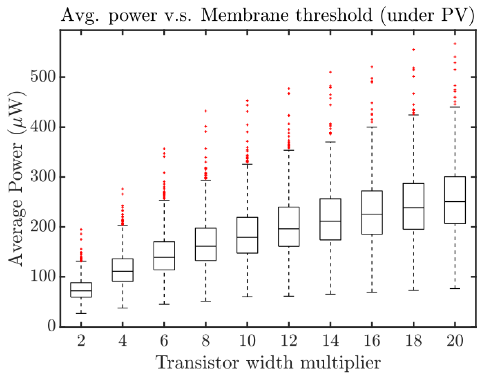
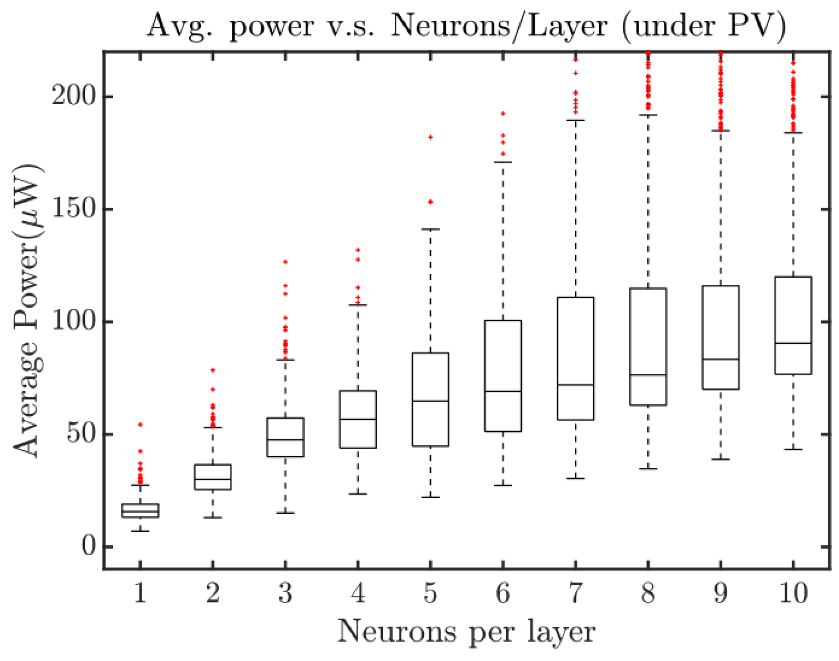
Note that process variations (PVs) in synapses and neurons can lead to a faster or slower spiking and can affect the power profiles observed by the adversary. Therefore, we perform a 1000 point Monte Carlo analysis with 3 σ of 100 mV of each transistor’s switching threshold over a 100 μ s sampling window for two of the design parameters. Figure 13 depicts the average power results when the neuron membrane threshold ( V t h ) is varied from 0.57 V to 0.75 V. The results show a positive trend in the median average power as V t h is increased. Similarly, Figure 14 depicts the average power results when the number of neurons per layer is varied from 1 to 10. A similar positive trend in the median power is observed. Therefore, average power can still leak information. A sophisticated adversary who has access to ample resources can analyze 1000 copies of an SNN chip and generate a range of average powers to match with the generated PV templates.

5.3. Feasibility of SCANN

Scalability: This work analyzes a 3 × 3 SNN constructed with a flavor of leaky integrate and fire (LIF) analog neuron using all-to-all interconnections. The model is scaled up to 10 × 10 to analyze the effectiveness of SCANN. In real-world applications, SNNs may employ 100 s of neurons per layer. While an increased number of neurons increases the average power consumed, it does not eliminate the unique markers in the power profile caused by the SNN spiking activity. The adversary can still identify these unique markers in the power profile to extract the spiking rate of neuron layers. Furthermore, the templates used for SCANN attacks can also be extended to include unique markers for more than 3 layers.
Extension to emerging technologies: Integrate-and-fire neurons using emerging technology, such as memristors, were recently proposed in [29,30], where short voltage pulses (input spikes) are employed to increase the conductance of the memristor device. When the conductance reaches a critical value (threshold), the neuron fires a spike, and the conductance is reset. While the power markers found in the power profile of memristor neuron-based SNNs may look different, SCANN attacks can still be applied to extract design parameters by generating power marker and average power templates.

5.4. Impact of Inputs and Connectivity

This paper assumes that (a) each neuron is fed by the same input and (b) the neurons are fully connected for the side channel analysis. These assumptions hold true if the adversary has physical possession of the chip and/or control over the inputs and the SNN architecture is fully connected. However, it should be noted that the spiking activity of the neurons of an SNN depends on the user input and the number of connections each neuron receives. The spiking rate and the average power may differ depending upon the user input and the connection type. An adversarial template is therefore valid only for a specific input pattern and interconnection architecture. The adversary has to generate multiple templates for different commonly implemented interconnection techniques.

5.5. Defenses against SCANN

Following approaches can be used to defend SNN’s against SCA:
Exploiting Transistor Variability: It was noted in Section 4 that the DC current through the neuron amplifier inverter is the primary source of side channel leakage. Therefore, decorrelating the spike rate with the DC current can obfuscate the side channel effectively. Since process variations are more prominent on the threshold voltages of smaller-sized transistors, one can design the amplifier’s inverter with smaller transistors to make it more sensitive to process variation. As a result, the switching threshold of the neuron will vary within-chip and chip-to-chip. If the switching threshold is higher, the DC current will be lower, even though the spike rate is slower at the neuron input. Therefore, the correlation with pre-calculated templates will be lost. Figure 15a depicts the change in average power as all the synaptic weights are varied from 1 M Ω to 10 M Ω in an SNN with large variation in the threshold voltage neuron amplifier transistors. It is seen that the median power in all cases remain mostly identical. Although effective, the variation in switching threshold due to PV may affect the accuracy and performance of the implemented SNN. Therefore, trade-offs among security, accuracy and performance should be considered carefully.
Power Camouflaging: Another technique to camouflage the SNN power profile without affecting its accuracy or performance is by introducing a few dummy neurons within each neuron layer (Figure 15b). The input of the dummy neurons is connected to a current driver that drives randomized spike inputs of 1 V amplitude and 50 ns spike width. These dummy neurons are not connected to any of the functioning neurons in the SNN and do not affect SNN accuracy or performance. However, they draw power from the supply in a randomized manner and generate rogue spike markers in the SNN power profile. Additionally, they also increase the average power consumption of the SNN and camouflage the original power features. Figure 15c depicts the difference in average power between the original SNN and a camouflaged SNN with 10% additional dummy neurons. It is seen that the amplitude and trendline of the average power are attenuated for the camouflaged SNN. Note that this defense increases the overall power consumption of the SNN design by ∼10%.

6. Conclusions

We present a detailed analysis of power and timing side channel leakage in spiking neural networks using a common analog neuron model and uncover several markers in the power profile. We also present eight unique reverse engineering techniques to identify four different critical design parameters, namely (a) synaptic weights, (b) neuron threshold, (c) neurons per layer, and (d) membrane capacitance. Finally, we proposed defenses against the proposed SCA attacks.

Author Contributions

Conceptualization, K.N. and S.G.; methodology, K.N, R.R., R.O.T., S.K. and S.G.; software, K.N. and R.R.; validation, K.N. and R.R.; formal analysis, K.N. and R.R.; investigation, K.N. and R.R.; writing—original draft preparation, K.N. and R.R.; writing—review and editing, K.N, R.R., R.O.T., S.K. and S.G.; visualization, K.N. and R.R.; supervision, S.G.; project administration, S.G.; funding acquisition, S.G. All authors have read and agreed to the published version of the manuscript.

Funding

This work is supported by SRC (2847.001) and NSF (CNS-1722557, CCF-1718474, DGE-1723687 and DGE-1821766).

Conflicts of Interest

The authors declare no conflict of interest. The funders had no role in the design of the study; in the collection, analyses, or interpretation of data; in the writing of the manuscript; or in the decision to publish the results.

References

  1. Kaiser, J.; Tieck, J.C.V.; Hubschneider, C.; Wolf, P.; Weber, M.; Hoff, M.; Friedrich, A.; Wojtasik, K.; Roennau, A.; Kohlhaas, R.; et al. Towards a framework for end-to-end control of a simulated vehicle with spiking neural networks. In Proceedings of the 2016 IEEE International Conference on Simulation, Modeling, and Programming for Autonomous Robots (SIMPAR), San Francisco, CA, USA, 13–16 December 2016; pp. 127–134. [Google Scholar]
  2. Azghadi, M.R.; Lammie, C.; Eshraghian, J.K.; Payvand, M.; Donati, E.; Linares-Barranco, B.; Indiveri, G. Hardware implementation of deep network accelerators towards healthcare and biomedical applications. IEEE Trans. Biomed. Circuits Syst. 2020, 14, 1138–1159. [Google Scholar] [CrossRef] [PubMed]
  3. Whatmough, P.N.; Lee, S.K.; Brooks, D.; Wei, G.Y. DNN engine: A 28-nm timing-error tolerant sparse deep neural network processor for IoT applications. IEEE J. -Solid-State Circuits 2018, 53, 2722–2731. [Google Scholar] [CrossRef]
  4. Cao, Y.; Chen, Y.; Khosla, D. Spiking deep convolutional neural networks for energy-efficient object recognition. Int. J. Comput. Vis. 2015, 113, 54–66. [Google Scholar] [CrossRef]
  5. Maass, W. Networks of spiking neurons: The third generation of neural network models. Neural Netw. 1997, 10, 1659–1671. [Google Scholar] [CrossRef]
  6. Heiberg, T.; Kriener, B.; Tetzlaff, T.; Einevoll, G.T.; Plesser, H.E. Firing-rate models for neurons with a broad repertoire of spiking behaviors. J. Comput. Neurosci. 2018, 45, 103–132. [Google Scholar] [CrossRef] [PubMed] [Green Version]
  7. Merolla, P.A.; Arthur, J.V.; Alvarez-Icaza, R.; Cassidy, A.S.; Sawada, J.; Akopyan, F.; Jackson, B.L.; Imam, N.; Guo, C.; Nakamura, Y.; et al. A million spiking-neuron integrated circuit with a scalable communication network and interface. Science 2014, 345, 668–673. [Google Scholar] [CrossRef] [PubMed]
  8. Davies, M.; Srinivasa, N.; Lin, T.H.; Chinya, G.; Cao, Y.; Choday, S.H.; Dimou, G.; Joshi, P.; Imam, N.; Jain, S.; et al. Loihi: A neuromorphic manycore processor with on-chip learning. IEEE Micro 2018, 38, 82–99. [Google Scholar] [CrossRef]
  9. Tavanaei, A.; Ghodrati, M.; Kheradpisheh, S.R.; Masquelier, T.; Maida, A. Deep learning in spiking neural networks. Neural Netw. 2019, 111, 47–63. [Google Scholar] [CrossRef] [PubMed] [Green Version]
  10. Bagheri, A.; Simeone, O.; Rajendran, B. Adversarial training for probabilistic spiking neural networks. In Proceedings of the 2018 IEEE 19th International Workshop on Signal Processing Advances in Wireless Communications (SPAWC), Kalamata, Greece, 25–28 June 2018; pp. 1–5. [Google Scholar]
  11. Venceslai, V.; Marchisio, A.; Alouani, I.; Martina, M.; Shafique, M. Neuroattack: Undermining spiking neural networks security through externally triggered bit-flips. In Proceedings of the 2020 International Joint Conference on Neural Networks (IJCNN), Glasgow, UK, 19–24 July 2020; pp. 1–8. [Google Scholar]
  12. Marchisio, A.; Nanfa, G.; Khalid, F.; Hanif, M.A.; Martina, M.; Shafique, M. Is spiking secure? A comparative study on the security vulnerabilities of spiking and deep neural networks. In Proceedings of the 2020 International Joint Conference on Neural Networks (IJCNN), Glasgow, UK, 19–24 July 2020; pp. 1–8. [Google Scholar]
  13. Nagarajan, K.; Li, J.; Ensan, S.S.; Kannan, S.; Ghosh, S. Fault injection attacks in spiking neural networks and countermeasures. Front. Nanotechnol. 2022, 3, 801999. [Google Scholar] [CrossRef]
  14. Nagarajan, K.; Li, J.; Ensan, S.S.; Khan, M.N.I.; Kannan, S.; Ghosh, S. Analysis of power-oriented fault injection attacks on spiking neural networks. In Proceedings of the 2022 Design, Automation & Test in Europe Conference & Exhibition (DATE), Antwerp, Belgium, 14–23 March 2022; pp. 861–866. [Google Scholar]
  15. Kocher, P.; Jaffe, J.; Jun, B. Differential power analysis. In Proceedings of the Annual International Cryptology Conference, Santa Barbara, CA, USA, 15–18 August 1999; pp. 388–397. [Google Scholar]
  16. Brier, E.; Clavier, C.; Olivier, F. Optimal statistical power analysis. In Cryptology ePrint Archive; International Association for Cryptologic Research: Bellevue, WA, USA, 2003. [Google Scholar]
  17. Kocher, P.C. Timing Attacks on Implementations of Diffie-Hellman, RSA, DSS, and Other Systems. In Proceedings of the Advances in Cryptology—CRYPTO ’96, Santa Barbara, CA, USA, 18–22 August 1996; Koblitz, N., Ed.; Springer: Berlin/Heidelberg, Germany, 1996; pp. 104–113. [Google Scholar]
  18. Brumley, D.; Boneh, D. Remote timing attacks are practical. Comput. Netw. 2005, 48, 701–716. [Google Scholar] [CrossRef]
  19. Quisquater, J.J.; Samyde, D. Electromagnetic analysis (ema): Measures and counter-measures for smart cards. In Proceedings of the International Conference on Research in Smart Cards, Cannes, France, 19–21 September 2001; Springer: Berlin/Heidelberg, Germany, 2001; pp. 200–210. [Google Scholar]
  20. Gandolfi, K.; Mourtel, C.; Olivier, F. Electromagnetic analysis: Concrete results. In Proceedings of the International Workshop on Cryptographic Hardware and Embedded Systems, Taipei, Taiwan, 25–28 September 2017; Springer: Berlin/Heidelberg, Germany, 2001; pp. 251–261. [Google Scholar]
  21. Batina, L.; Bhasin, S.; Jap, D.; Picek, S. CSI neural network: Using side-channels to recover your artificial neural network information. arXiv 2018, arXiv:1810.09076. [Google Scholar]
  22. Garaffa, L.C.; Aljuffri, A.; Reinbrecht, C.; Hamdioui, S.; Taouil, M.; Sepulveda, J. Revealing the Secrets of Spiking Neural Networks: The Case of Izhikevich Neuron. In Proceedings of the 2021 24th Euromicro Conference on Digital System Design (DSD), Palermo, Spain, 1–3 September 2021; pp. 514–518. [Google Scholar]
  23. Indiveri, G.; Linares-Barranco, B.; Hamilton, T.J.; Schaik, A.v.; Etienne-Cummings, R.; Delbruck, T.; Liu, S.C.; Dudek, P.; Häfliger, P.; Renaud, S.; et al. Neuromorphic silicon neuron circuits. Front. Neurosci. 2011, 5, 73. [Google Scholar] [CrossRef] [PubMed] [Green Version]
  24. Alibart, F.; Pleutin, S.; Guérin, D.; Novembre, C.; Lenfant, S.; Lmimouni, K.; Gamrat, C.; Vuillaume, D. An organic nanoparticle transistor behaving as a biological spiking synapse. Adv. Funct. Mater. 2010, 20, 330–337. [Google Scholar] [CrossRef] [Green Version]
  25. Abu-Hassan, K.; Taylor, J.D.; Morris, P.G.; Donati, E.; Bortolotto, Z.A.; Indiveri, G.; Paton, J.F.; Nogaret, A. Optimal solid state neurons. Nat. Commun. 2019, 10, 5309. [Google Scholar] [CrossRef] [Green Version]
  26. Gkoupidenis, P.; Schaefer, N.; Garlan, B.; Malliaras, G.G. Neuromorphic functions in PEDOT: PSS organic electrochemical transistors. Adv. Mater. 2015, 27, 7176–7180. [Google Scholar] [CrossRef]
  27. Nawrocki, R.A.; Voyles, R.M.; Shaheen, S.E. Neurons in polymer: Hardware neural units based on polymer memristive devices and polymer transistors. IEEE Trans. Electron Devices 2014, 61, 3513–3519. [Google Scholar] [CrossRef]
  28. Mead, C.; Ismail, M. Analog VLSI Implementation of Neural Systems; Springer: Berlin/Heidelberg, Germany, 1989; Volume 80. [Google Scholar]
  29. Mehonic, A.; Kenyon, A.J. Emulating the electrical activity of the neuron using a silicon oxide RRAM cell. Front. Neurosci. 2016, 10, 57. [Google Scholar] [CrossRef] [PubMed]
  30. Lashkare, S.; Chouhan, S.; Chavan, T.; Bhat, A.; Kumbhare, P.; Ganguly, U. PCMO RRAM for integrate-and-fire neuron in spiking neural networks. IEEE Electron Device Lett. 2018, 39, 484–487. [Google Scholar] [CrossRef]
Figure 1. Threat model showing progression of power-based SCA on SNN.
Cryptography 07 00017 g001
Figure 2. (a) Axon hillock circuit; and (b) simulation result of axon hillock spike generation showing input current ( I i n ) (top plot), the membrane voltage ( V m e m ) and the output voltage ( V o u t ) (bottom plot).
Cryptography 07 00017 g002
Figure 3. Baseline 2-layer 3 × 3 SNN implemented for power SCA.
Cryptography 07 00017 g003
Figure 4. (a) SNN current profile for a 3 × 3 SNN depicting input spikes, and output spikes of layer-1 and layer-2 neurons; and (b) zoomed-in SNN power profile depicting power characteristics caused by corresponding input and output spikes.
Cryptography 07 00017 g004
Figure 5. Markers in the power profile revealing the layer and type of voltage spikes in a 3 × 3 SNN architecture.
Cryptography 07 00017 g005
Figure 6. SCANN 1: (a) SNN Layer-2 neuron’s spiking activity (boxed in red and green) and overall current profile in a 3 × 3 network under different input synaptic weights; (b) effect of synaptic weights on neuron’s time-to-spike; and (c) effect of synaptic weights on number of Layer-2 output spikes in a 50 μ s window.
Cryptography 07 00017 g006
Figure 7. Effect of NMOS ( M N 3 ) and PMOS ( M P 1 ) transistor widths on neuron membrane threshold.
Cryptography 07 00017 g007
Figure 8. SCANN 2: (a) Power profiles with markers revealing output neuron’s spike time (boxed in red) under different neuron thresholds; (b) effect of output neuron’s membrane threshold on neuron’s time-to-spike; and (c) effect of membrane output neuron’s membrane threshold on number of Layer-2 output spikes in a 50 μ s window.
Cryptography 07 00017 g008
Figure 9. SCANN 3: (a) Power profiles with markers revealing output neuron’s spike time (boxed in red) under different number of neurons/layer; (b) effect of neurons per layer on neuron’s time-to-spike; and (c) effect of neurons per layer on number of Layer-2 output spikes in a 50 μ s window.
Cryptography 07 00017 g009
Figure 10. SCANN 4: (a) Power profiles with markers revealing output neuron’s spike time (boxed in red) under different membrane capacitances; (b) effect of membrane capacitance on neuron’s time-to-spike; and (c) effect of membrane capacitance on number of Layer-2 output spikes in a 50 μ s window.
Cryptography 07 00017 g010
Figure 11. SCANN 5: Average SNN power as different percentages of synapses and varied from 1 M Ω to 10 M Ω in a sampling window of (a) 25 μ s; (b) 50 μ s; and (c) 100 μ s (with 1 M Ω as baseline synaptic weight).
Cryptography 07 00017 g011
Figure 12. Average SNN power in sampling windows ranging from 25 μ s to 500 μ s while varying (a) neuron threshold (SCANN 6) (b) number of neurons per layer (SCANN 7); and (c) neuron’s membrane capacitance (SCANN 8).
Cryptography 07 00017 g012
Figure 13. Effect of neuron membrane threshold on average power under PV.
Cryptography 07 00017 g013
Figure 14. Effect of neurons per layer on average power under PV.
Cryptography 07 00017 g014
Figure 15. (a) Effect of synaptic weight on average power under defensive transistor sizing and PV; (b) power camouflaging using dummy neurons; and (c) comparison of change in average power between original SNN and camouflaged SNN with dummy neurons.
Cryptography 07 00017 g015
Table 1. Summary of SCANN attacks.
SNN Design ParameterSpike Rate
(SCANN 1–4)
Average Power
(SCANN 5–8)
Synapse Weight
Neuron Threshold
Neurons/Layer
Neuron Capacitance
Disclaimer/Publisher’s Note: The statements, opinions and data contained in all publications are solely those of the individual author(s) and contributor(s) and not of MDPI and/or the editor(s). MDPI and/or the editor(s) disclaim responsibility for any injury to people or property resulting from any ideas, methods, instructions or products referred to in the content.