Miniaturized On-Chip NFC Antenna versus Screen-Printed Antenna for the Flexible Disposable Sensor Strips


Abstract
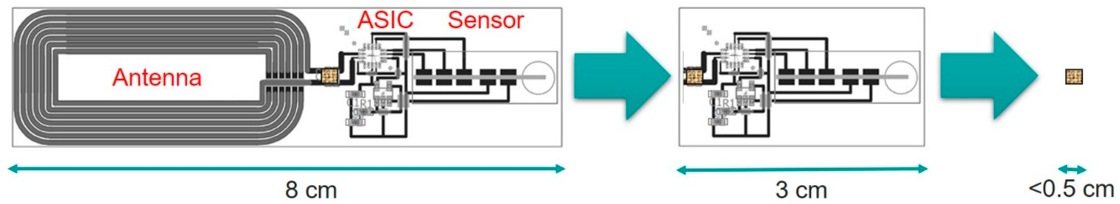
1. Introduction
2. Methods
- (a)
- On-chip antenna (fabricated and simulated)
- (b)
- On-chip antenna with ferrite layer (simulated)
- (c)
- On-substrate screen-printed Ag antenna on paper (fabricated and simulated)
- (d)
- On-substrate Cu-etched antenna on PCB (fabricated and simulated)
3. Results and Discussion
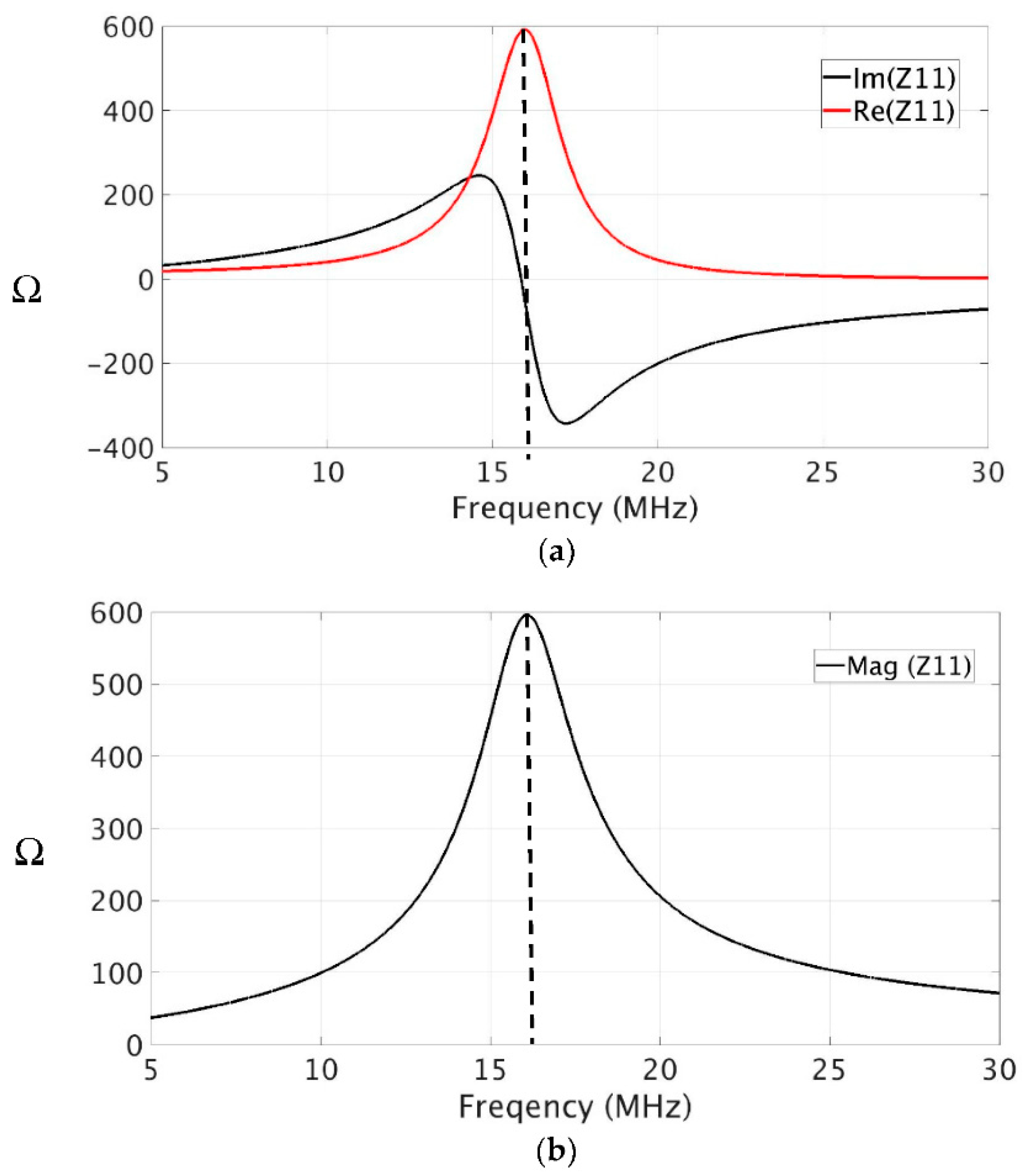
3.1. The Performance of On-Chip NFC Antenna
3.2. The Effect of Conductor Materials and Thicknesses
3.3. The Effect of Double-Layering
3.4. Investigating the Effects of Ferrite
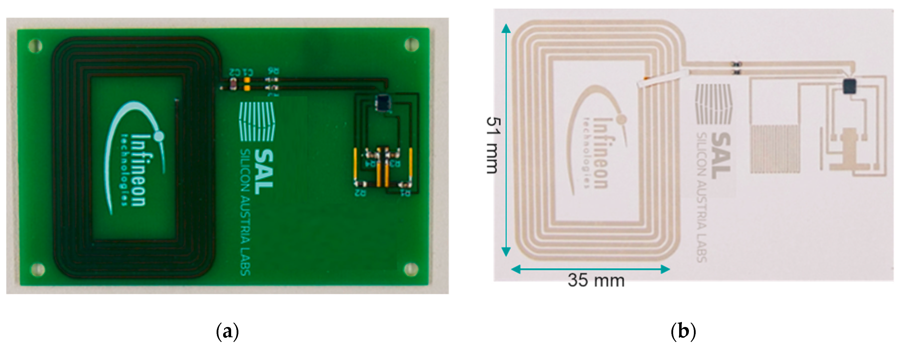
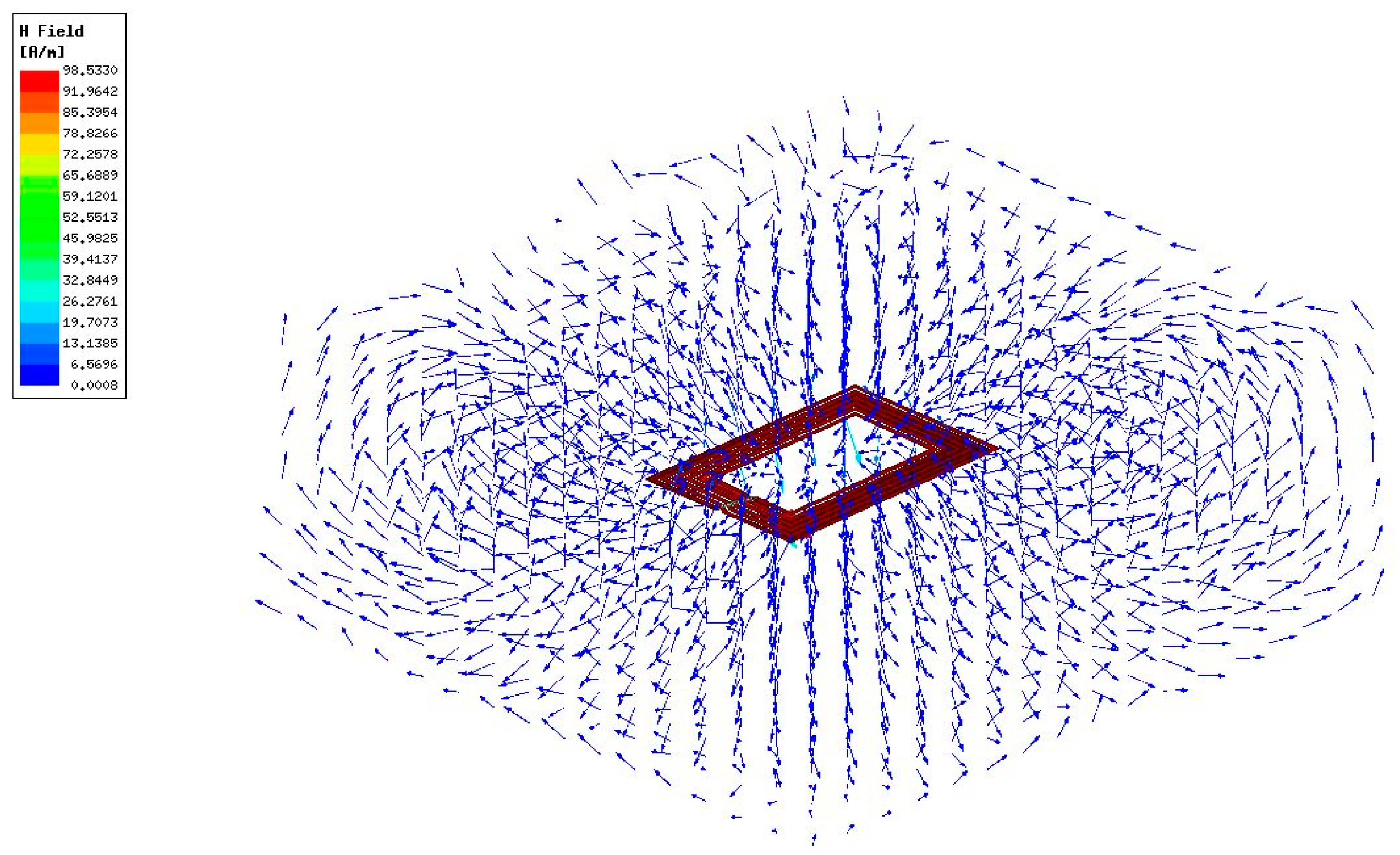
3.5. On-Substrate Antennas
3.6. Coupling of Antennas
4. Conclusions
Author Contributions
Funding
Acknowledgments
Conflicts of Interest
References
- Aziza, H. NFC technology in mobile phone next-generation service. In Proceedings of the 2010 Second International Workshop on Near Field Communication (NFC), Monaco, Monaco, 20–22 April 2010; pp. 21–26. [Google Scholar]
- Kollegger, C.; Greiner, P.; Siegl, I.; Steffan, C.; Wiessflecker, M.; Pekec, B.; Hajnsek, M.; Sinner, F.; Holweg, G.; Deutschmann, B. Intelligent NFC potassium measurement strip with hemolysis check in capillary blood. Elektrotech. Inf. 2018, 135, 83–88. [Google Scholar] [CrossRef]
- Pachler, W.; Bösch, W.; Holweg, G.; Hofer, G. Novel booster antenna design coupled to a one square millimeter coil-on-chip RFID tag enabling new medical applications. In Proceedings of the 43rd European Microwave Conference, Nuremberg, Germany, 7–10 October 2013. [Google Scholar]
- Grosinger, J.; Pachler, W.; Bosch, W. Tag Size Matters: Miniaturized RFID Tags to Connect Smart Objects to the Internet. IEEE Microw. Mag. 2018, 19, 101–111. [Google Scholar] [CrossRef]
- Pozar, D.M. Microwave Engineering, 4th ed.; John Wiley & Sons, Inc.: Hoboken, NJ, USA, 2011; ISBN 978-0-470-63155-3. [Google Scholar]
- Lau, S.S. Practical design of 13.56MHz Near Field Communication (NFC) and Radio Frequency Identification (RFID) antenna using ferrite sheet on metallic surface by Network Analyzer. In Proceedings of the 2015 IEEE International Conference on Industrial Engineering and Engineering Management (IEEM), Singapore, 6–9 December 2015; pp. 1362–1366. [Google Scholar]
- Gebhart, M.; Neubauer, R.; Stark, M.; Warnez, D. Design of 13.56 MHz Smartcard Stickers with Ferrite for Payment and Authentication. In Proceedings of the 2011 Third International Workshop on Near Field Communication, Hagenberg, Austria, 22–23 February 2011; pp. 59–64. [Google Scholar] [CrossRef]
- Li, L.; Gao, Z.; Wang, Y. NFC antenna research and a simple impedance matching method. In Proceedings of the 2011 International Conference on Electronic & Mechanical Engineering and Information Technology, Harbin, China, 12–14 August 2011; pp. 3968–3972. [Google Scholar] [CrossRef]
- Pachler, W.; Grosinger, J.; Bösch, W.; Holweg, G.; Popovic, K.; Blümel, A.; List-Kratochvil, E.J. A silver inkjet printed ferrite NFC antenna. In Proceedings of the 2014 Loughborough Antennas and Propagation Conference (LAPC), Loughborough, UK, 10–11 November 2014; pp. 95–99. [Google Scholar] [CrossRef]
- Nie, S.J.; Geng, H.; Wang, J.B.; Wang, L.S.; Wang, Z.W.; Xu, R.; Yue, G.H.; Chen, Y.Z.; Peng, D.L. The Structure and Magnetic Properties of NiZn-Ferrite Films Deposited by Magnetron Sputtering at Room Temperature. Adv. Mater. Res. 2013, 690–693, 1702–1706. [Google Scholar] [CrossRef]
- Roshanghias, A.; Rodrigues, A.D.; Holzmann, D. Thermosonic fine-pitch flipchip bonding of silicon chips on screen printed paper and PET substrates. Microelectron. Eng. 2020, 228, 111330. [Google Scholar] [CrossRef]
- Yusuf, Y.; Kanagesan, S.; Bahmanrokh, G. Microstructure and magnetic properties of Ni-Zn ferrite thin film synthesized using sol-gel and spin-coating technique. J. Aust. Ceram. Soc. 2017, 53, 767–774. [Google Scholar] [CrossRef]
- Yusuf, Y.; Mustaffa, M.S. Spin-Coating Technique for Fabricating Nickel Zinc Nanoferrite (Ni0. 3Zn0. 7Fe2O4) Thin Films. In Coatings and Thin-Film Technologies; IntechOpen: London, UK, 2018. [Google Scholar]
- Lim, C.C.; Yeo, K.S.; Chew, K.W.; Cabuk, A.; Gu, J.M.; Lim, S.F.; Boon, C.C.; Do, M.A. Fully Symmetrical Monolithic Transformer (True 1:1) for SiliconRFIC. IEEE Trans. Microw. Theory Tech. 2008, 56, 2301–2311. [Google Scholar]
- Zargham, M.; Gulak, P.G. Maximum Achievable Efficiency in Near-Field Coupled Power-Transfer Systems. IEEE Trans. Biomed. Circ. Syst. 2012, 6, 228–245. [Google Scholar] [CrossRef] [PubMed]


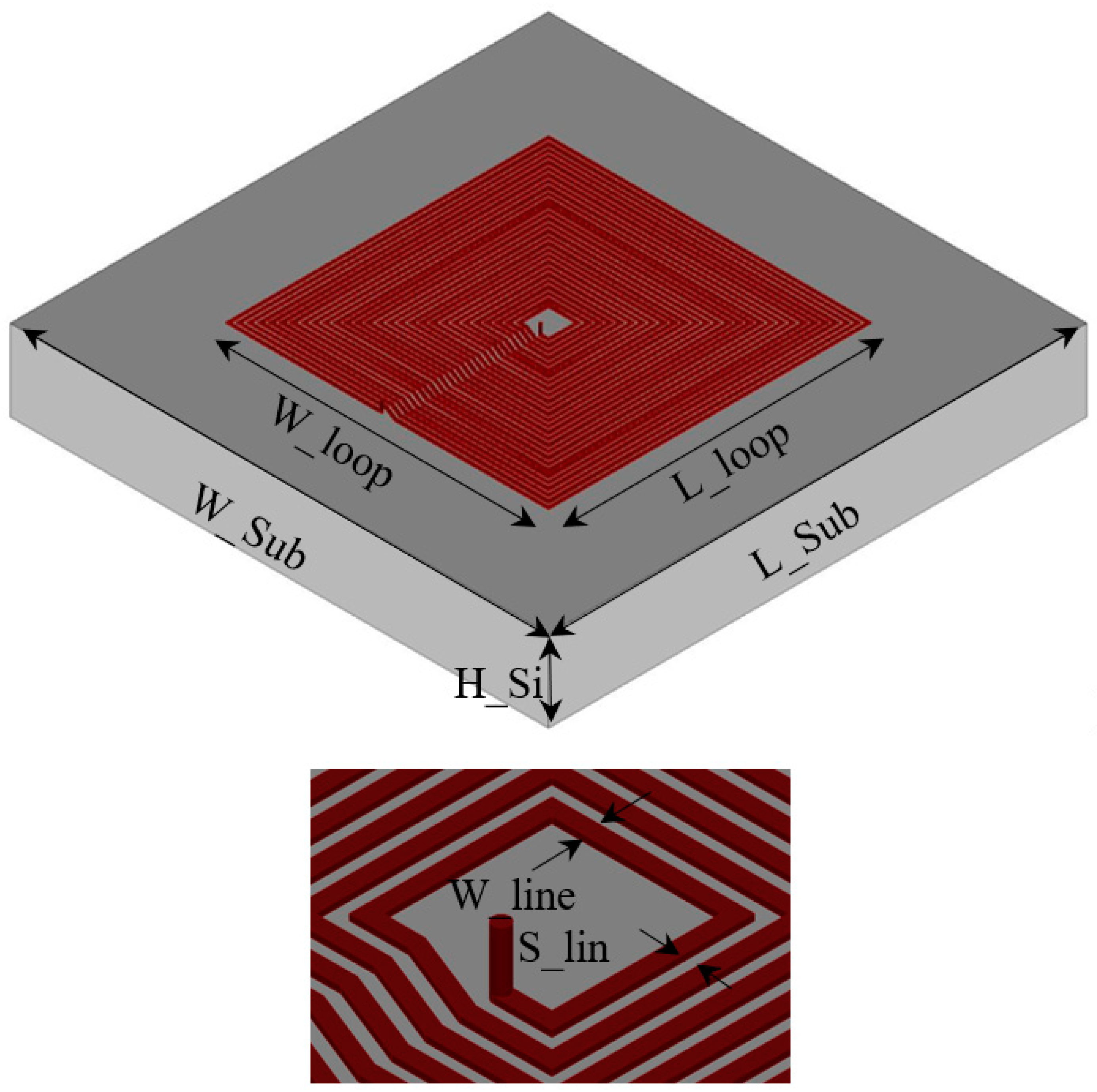
| W_Sub | L_Sub | W_Loop | L_Loop | W_Line | S_Line | H_Si | H_SiNi | H_Copper |
|---|---|---|---|---|---|---|---|---|
| 4 mm | 4 mm | 2.4 mm | 2.4 mm | 20 µm | 20 µm | 600 µm | 500 nm | 8 µm |
| R (Ω) | L (µH) | |
|---|---|---|
| Aluminum 1 µm | 163 | 0.790 |
| Aluminum 5 µm | 33 | 0.821 |
| Aluminum 10 µm | 16.8 | 0.815 |
| Copper 1 µm | 107 | 0.809 |
| R (Ω) | L (µH) | |
|---|---|---|
| Without ferrite | 15.7 | 0.922 |
| 1 µm thick ferrite (σ = 0.01 S/m) | 17.8 | 1.420 |
| 1 µm thick ferrite (σ = 0.1 S/m) | 19.5 | 1.414 |
| 10 µm thick ferrite (σ = 0.01 S/m) | 18.1 | 1.748 |
| R (Ω) | L (µH) | |
|---|---|---|
| PCB (etched Cu antenna with the thickness of 35 µm) | 1.09 | 2.108 |
| E-paper (screen-printed Ag antenna with a thickness of 10 µm) | 35 | 1.681 |
| Tag Coil Geometry | k [1] | ηmax [%] |
|---|---|---|
| Paper coil with silver conductor (Figure 6b) | 0.53 | 78.6 |
| Two-layer on-chip coil (Figure 4) | 0.013 | 0.651 |
| Single-layer on-chip coil | 0.015 | 0.617 |
| Single-layer on-chip coil with 1 µm ferrite | 0.012 | 0.571 |
| Tag Coil Geometry | ηeffective [%] |
|---|---|
| Single-layer on-chip coil | 0.11 |
| Single-layer on-chip coil with 1 µm ferrite layer | 0.16 |
| Two-layer on-chip coil | 0.12 |
Publisher’s Note: MDPI stays neutral with regard to jurisdictional claims in published maps and institutional affiliations. |
© 2020 by the authors. Licensee MDPI, Basel, Switzerland. This article is an open access article distributed under the terms and conditions of the Creative Commons Attribution (CC BY) license (http://creativecommons.org/licenses/by/4.0/).
Share and Cite
Kordzadeh, A.; Holzmann, D.; Binder, A.; Moldaschl, T.; Sturm, J.; Roshanghias, A. Miniaturized On-Chip NFC Antenna versus Screen-Printed Antenna for the Flexible Disposable Sensor Strips. IoT 2020, 1, 309-319. https://doi.org/10.3390/iot1020018
Kordzadeh A, Holzmann D, Binder A, Moldaschl T, Sturm J, Roshanghias A. Miniaturized On-Chip NFC Antenna versus Screen-Printed Antenna for the Flexible Disposable Sensor Strips. IoT. 2020; 1(2):309-319. https://doi.org/10.3390/iot1020018
Chicago/Turabian StyleKordzadeh, Atefeh, Dominik Holzmann, Alfred Binder, Thomas Moldaschl, Johannes Sturm, and Ali Roshanghias. 2020. "Miniaturized On-Chip NFC Antenna versus Screen-Printed Antenna for the Flexible Disposable Sensor Strips" IoT 1, no. 2: 309-319. https://doi.org/10.3390/iot1020018
APA StyleKordzadeh, A., Holzmann, D., Binder, A., Moldaschl, T., Sturm, J., & Roshanghias, A. (2020). Miniaturized On-Chip NFC Antenna versus Screen-Printed Antenna for the Flexible Disposable Sensor Strips. IoT, 1(2), 309-319. https://doi.org/10.3390/iot1020018