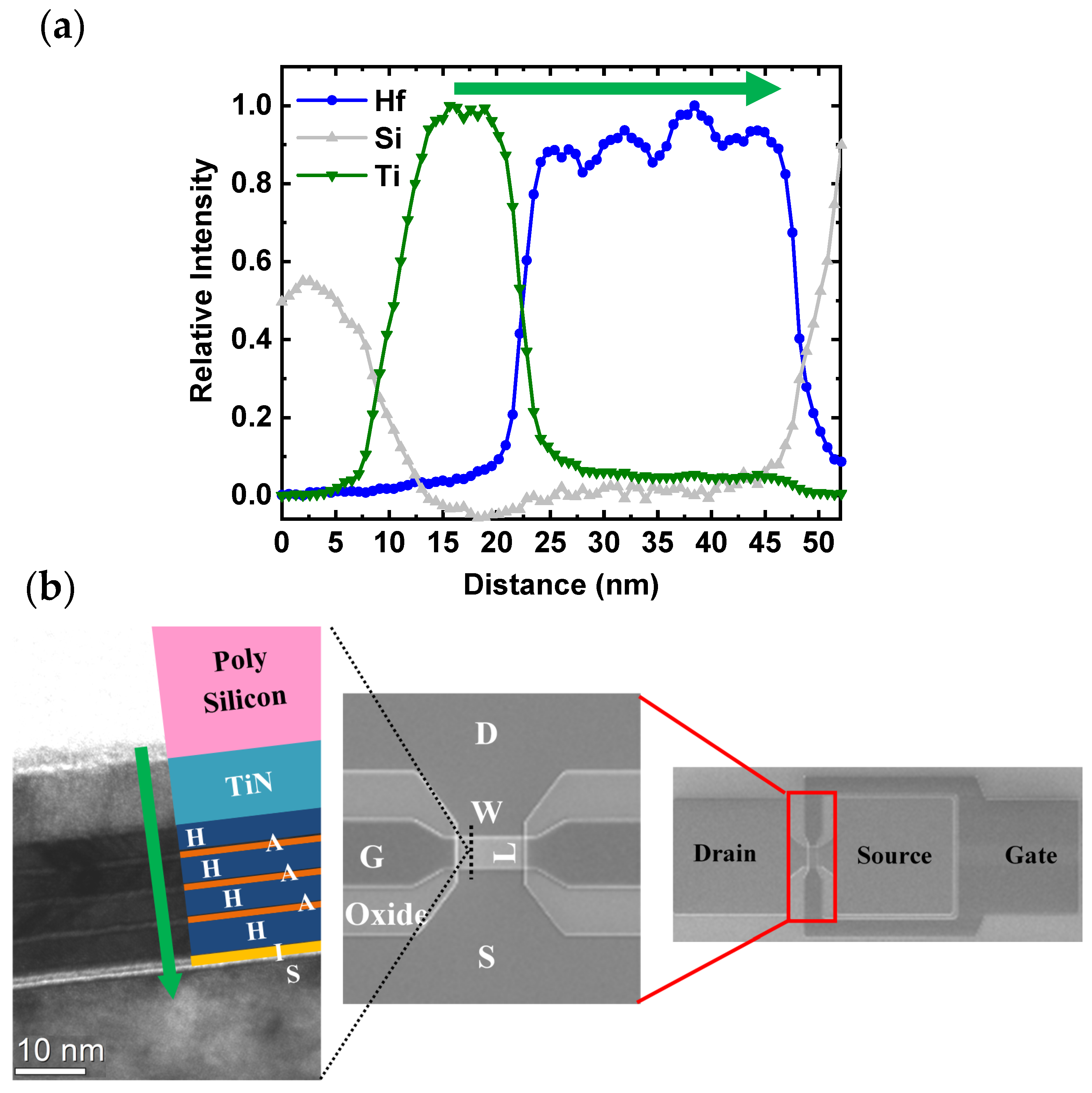
3.1. The Laminate MFM and Stack Characteristics
In an MFM structure, the P
r change over the ferroelectric thickness reflects the strong role of the film stress on the stabilization of the ferroelectric phase. In a thin ferroelectric film, the crystallization and thus the stabilized crystallographic phase is affected by the film stress induced by the metal electrodes. The metal electrodes provide a mechanical capping to prevent the volume expansion of the basic unit cell; this reduces the monoclinic phase formation as indicated in the first report by Böscke et al. [
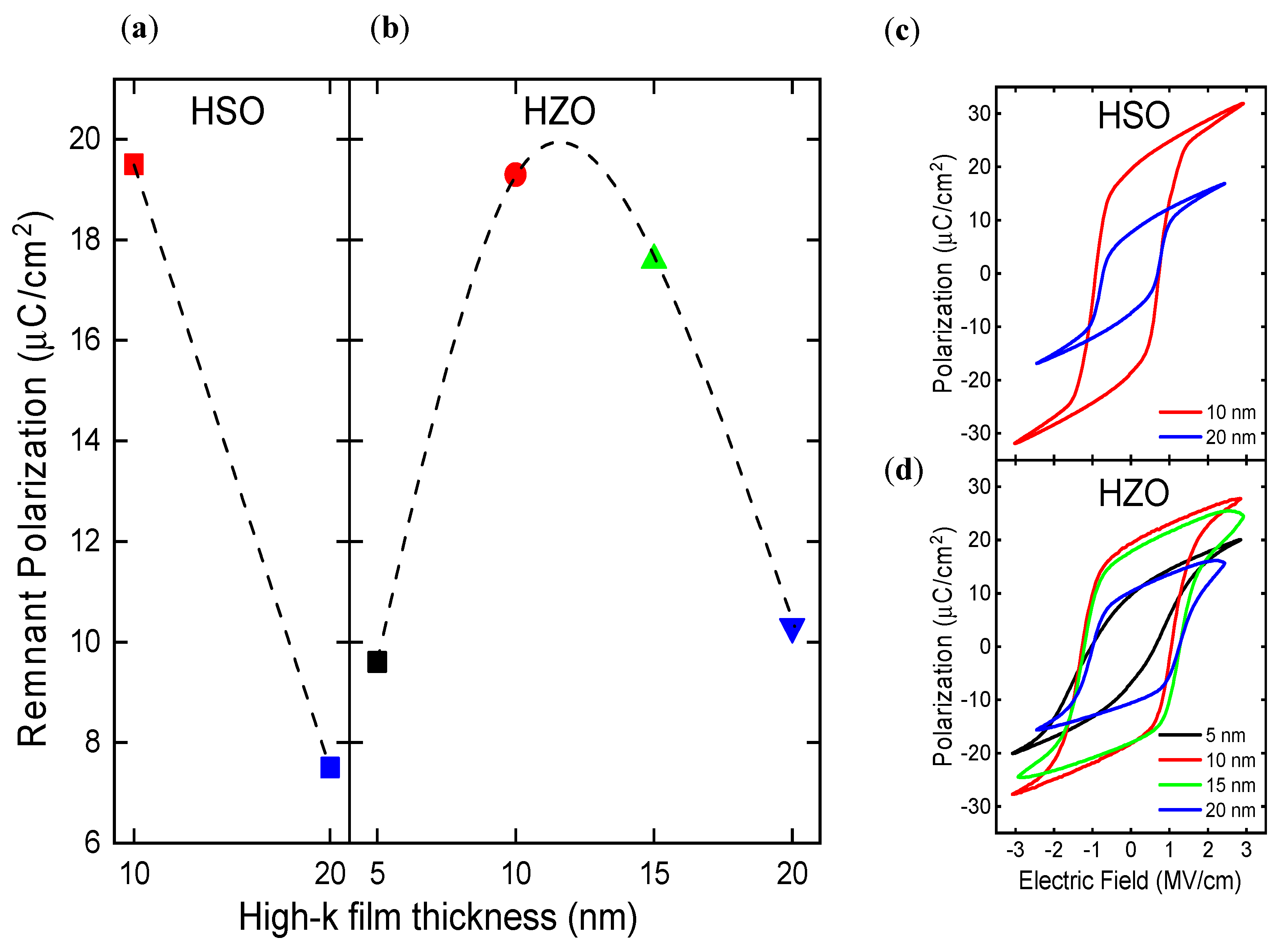
7]. The ferroelectric thickness variation also affects the average grain size formation and hence the ferroelectric properties. For HSO and HZO ferroelectrics, the ferroelectric properties were studied as shown in
Figure 4a,b for the P
r change in relation to the thickness and in
Figure 4c,d with the corresponding P-E hysteresis. The transition toward a thicker ferroelectric film of 20 nm showed a decrease in P
r, which was a consequence of an increased average grain size thus favoring the monoclinic phase formation [
20].
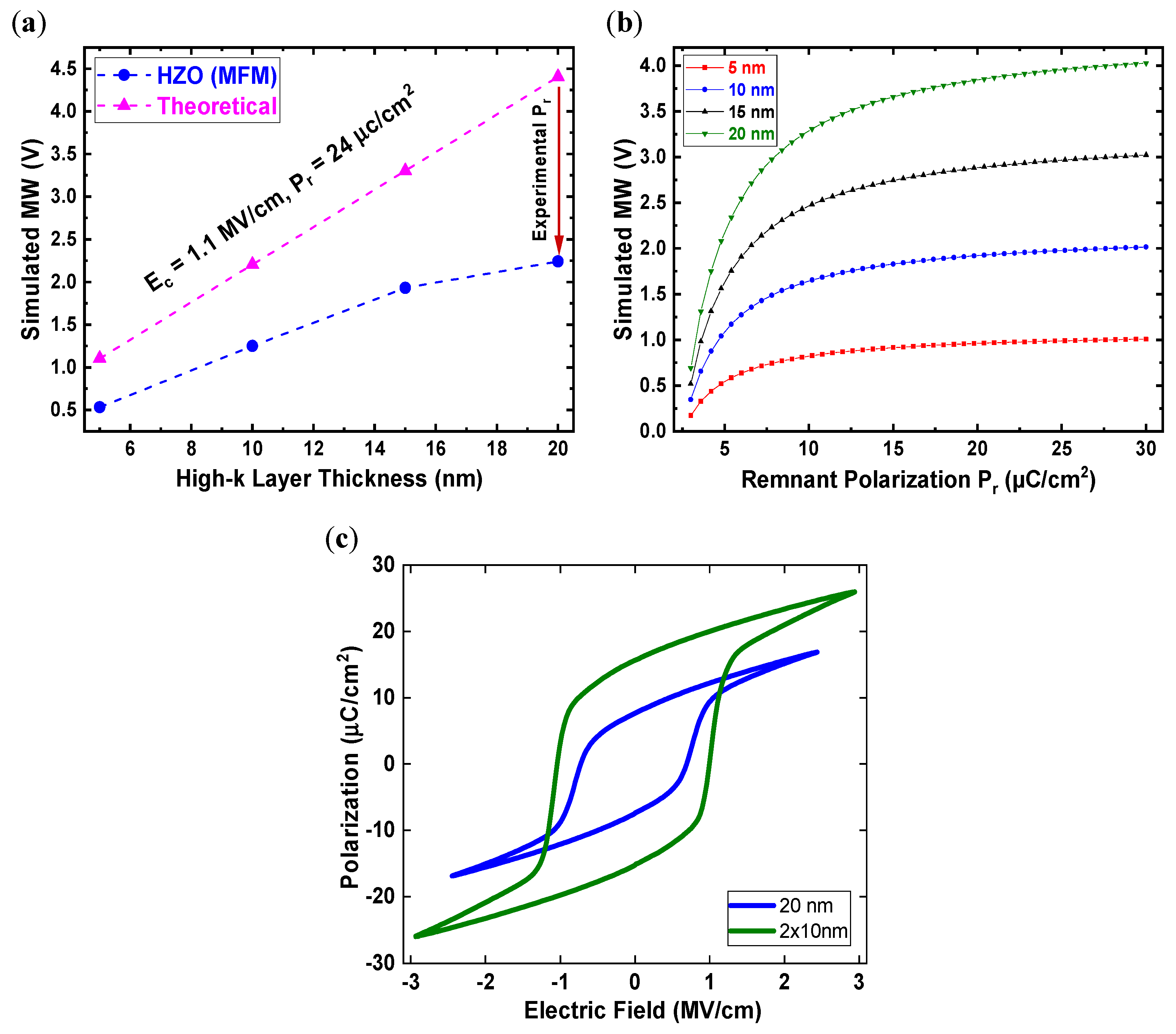
The numerical simulation of the FeFET memory was realized based on an iterative solution of the FET equation with the ferroelectric layer properties incorporated. This approach is central to theoretical FeFET modeling [
21,
22,
23]. The measured ferroelectric properties as P
r and E
c values of the HZO material (
Figure 4) were used in the FeFET numerical simulation to estimate the maximum MW of each ferroelectric layer thickness (
Figure 5a). In comparison, a saturated high P
r value (24 µC/cm
2) was used to indicate the potential theoretical reference for the maximum MW of each thickness (5 nm to 20 nm). The increase in the HZO ferroelectric layer thickness (
Figure 5a) shows that the calculated MW, based on the measured MFM P
r, was far lower than the theoretical one. This MW gap increased as the ferroelectric thickness increased as a manifestation of the critical P
r decrease. This reveals that the ferroelectric P
r is as an important parameter for achieving the target MW increase with increasing thickness as pointed out in
Figure 5b of the simulated MW dependence on the P
r for (5 nm to 20 nm) ferroelectric thickness. In the low range of P
r values (
Figure 5b), comparable to the ones measured in the MFM configuration (20 nm), the obtained MW becomes significantly lower than the saturated one. To preserve a high P
r at an increased ferroelectric thickness, the single ferroelectric layer (20 nm) was replaced by a laminate (2 × 10 nm) stack with an alumina interlayer. The polarization-electric field (P-E) hysteresis in
Figure 5c shows a comparison between the single ferroelectric layer and the laminate ferroelectric stack of the same HSO total ferroelectric thickness (20 nm). A higher P
r was achieved by the ferroelectric stack lamination.
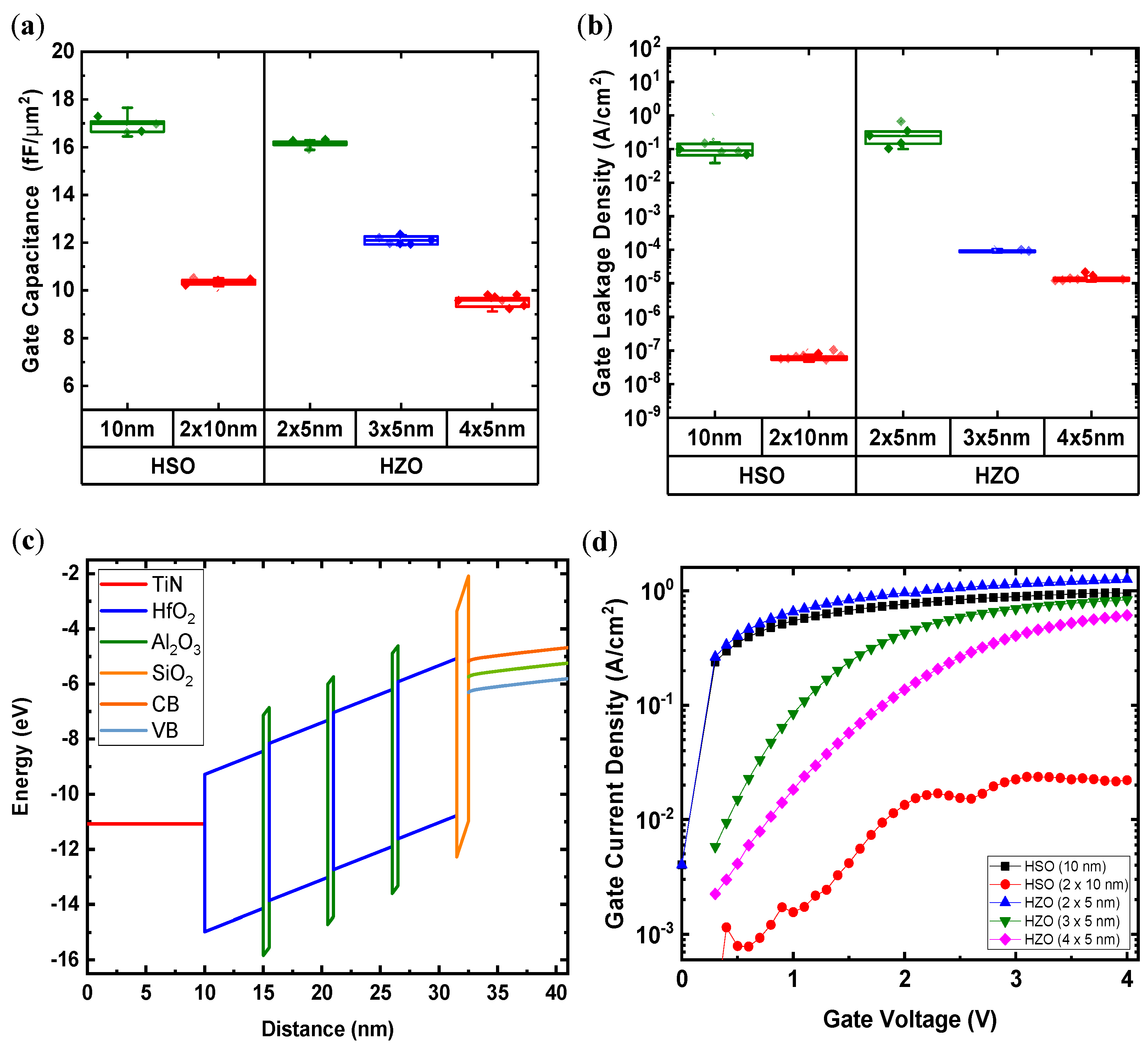
In addition, the ferroelectric lamination affected the basic metal-ferroelectric-insulator-semiconductor (MFIS) stack characteristics such as capacitance and leakage. The effect of ferroelectric lamination can be deduced in
Figure 6 from the measured stack capacitance per unit area in accumulation, as well as the current density of the stack leakage. The MFIS stack capacitance per unit area was measured on a capacitor of a 10
4 µm
2 size with a gate voltage sweep range (−5 V to 5 V) at a frequency of 3 KHz. The gate leakage current was measured on the same capacitor size via a gate voltage sweep (−0.2 V to 4 V) where the leakage current is extracted at a 3 V gate voltage. For a benchmark of the different ferroelectric stacks, the accumulation capacitance was extracted at a gate voltage (−3 V) and plotted in
Figure 6a for the HSO and HZO materials. Based on an identical interface layer (IL), a trend of decreased capacitance per unit area occurred as the ferroelectric stack thickness increased. Thereby, the difference in permittivity values as well as the count of alumina interlayers causes a lower HZO stack capacitance compared to the HSO one (
Figure 6a) at the same total stack thickness (e.g., 20 nm).
For the same SiN based IL, the capacitance change in
Figure 6a reflects the opposite trend of an increased operating voltage to achieve the same ferroelectric switching field, which is in part attributed to the lamination effect. Thus, the control of both the total stack thickness and the alumina interlayer count is an essential tradeoff for ferroelectric stack optimization. However, the key merit of the ferroelectric stack lamination is the decrease in the gate current density (
Figure 6b,d) that reflects both the effect of the lamination and the stack thickness increase. Due to the higher dielectric bandgap of the alumina interlayers, the ferroelectric stack lamination constitutes an alternative low-high dielectric band energy profile (
Figure 6c) that reduces the gate stack leakage density. In essence, a difference in the leakage properties between the HSO and HZO laminates (20 nm) indicates degraded HZO dielectric properties. This is mainly due to the associated gate first (1050 °C) thermal budget. Thereby, the HZO leakage effect is alleviated by the stack lamination.
3.2. The Laminate FeFET Memory Switching
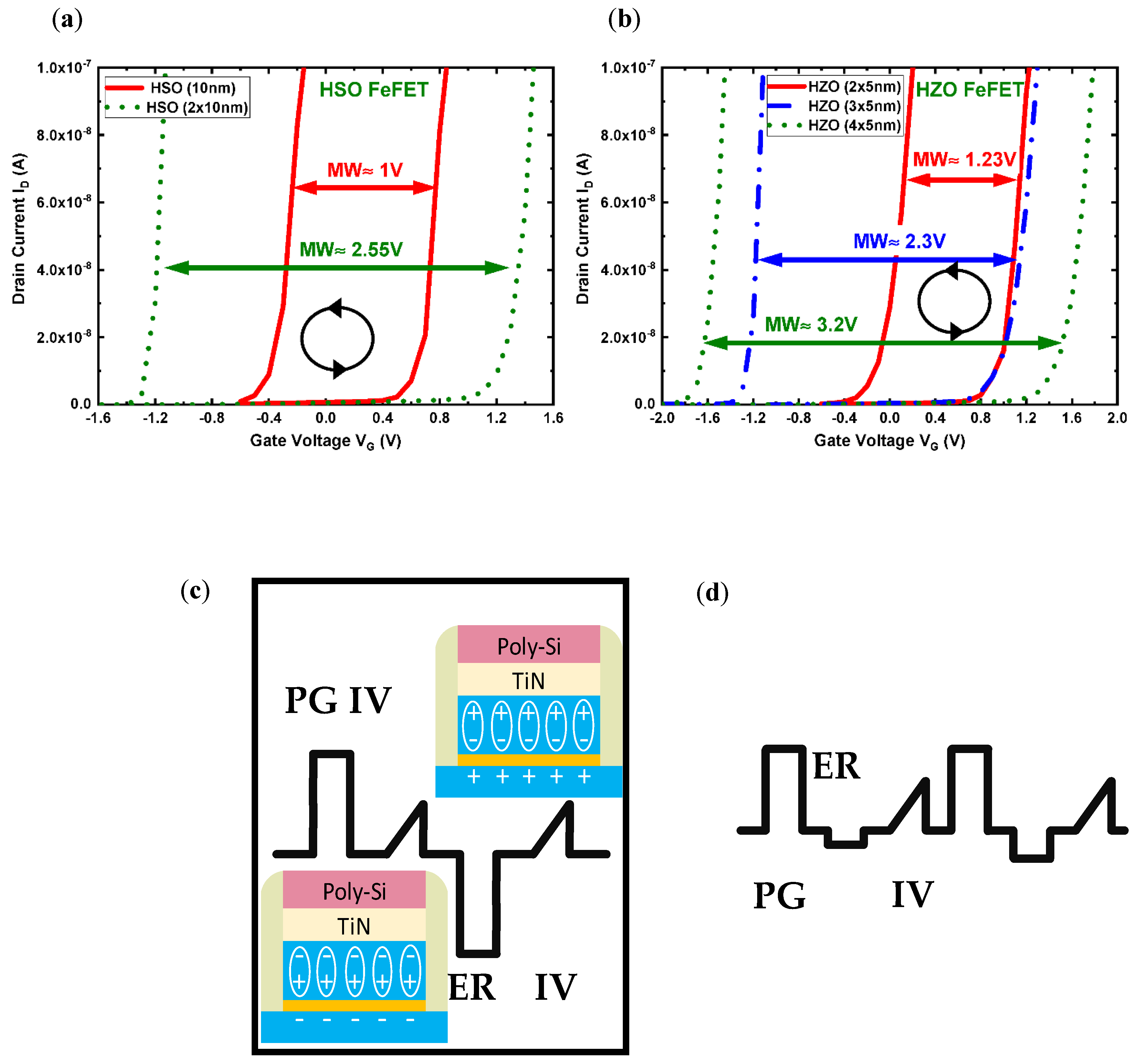
The reversible dipole switching has polarization charges that can modulate the channel conductivity. The program/erase (PG/ER) pulses (
Figure 7c) can reversibly switch the dipoles with the internal dipole field affecting the channel surface potential, hence the V
T shift. Thus, the laminate FeFET memory switches state after the PG/ER pulse which is measured by an I
D-V
G sweep where a counterclockwise switching i.e., a low/high (PG/ER) V
T shift, is observed as a sign of ferroelectric switching. This particular V
T shift direction occurs as the surface charges near the channel which modulate the extent of the channel inversion. However, this switching behavior is also dependent on the ferroelectric stack type as shown in
Figure 7a,b which illustrate a different MW size by varying the stack material type and thickness. The MW expression was considered with a detailed analytical treatment of the FeFET stack [
24] and is more commonly represented by Equation (1) which considers the remanent polarization (P
r), the coercive field (E
c), and thickness (d
F) as direct factors affecting the MW size.
The trend in
Figure 7a,b shows consistently the role of ferroelectric thickness increase in forming an MW of a higher size. This trend is reproducible for HSO and HZO materials. Although, for the same total ferroelectric stack thickness (e.g., 20 nm), a marked difference between the HSO and HZO can be observed. This indicates the different film properties of HSO and HZO and thus, suggests that other factors such as P
r and E
c can affect the MW size. The field-dependent evolution of ferroelectric switching as shown in
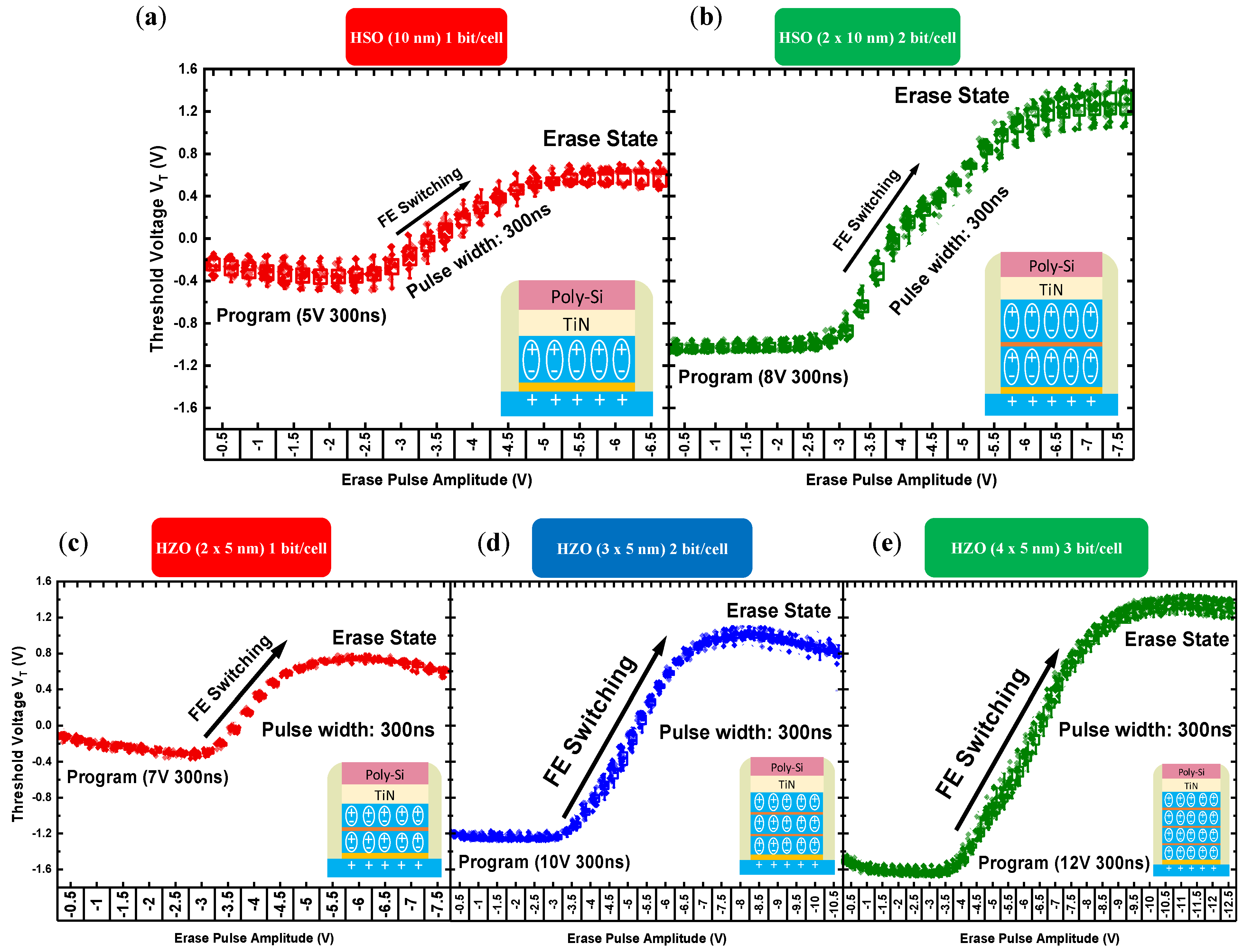
Figure 8 with an ER pulse amplitude increase gives a valuable insight into the MLC operation. The ER amplitude switching was measured on a device of width × length (W × L) (25 µm × 25 µm) with cross wafer statistics measured at a PG/ER pulse width (300 ns). By using a reference PG pulse while gradually increasing the ER pulse amplitude as depicted in
Figure 7d, the V
T shift was controlled to a target level in the MLC window. The PG low V
T gradually shifted toward the high V
T (ER state) after each increase in the amplitude of the ER pulse until a saturated ER switching was reached. Hence, the MLC capacity (bit/cell) is dependent on the maximum V
T shift (dynamic range), which is significantly improved by the ferroelectric stack lamination, thus enabling an MLC storage up to 3 bit/cell.
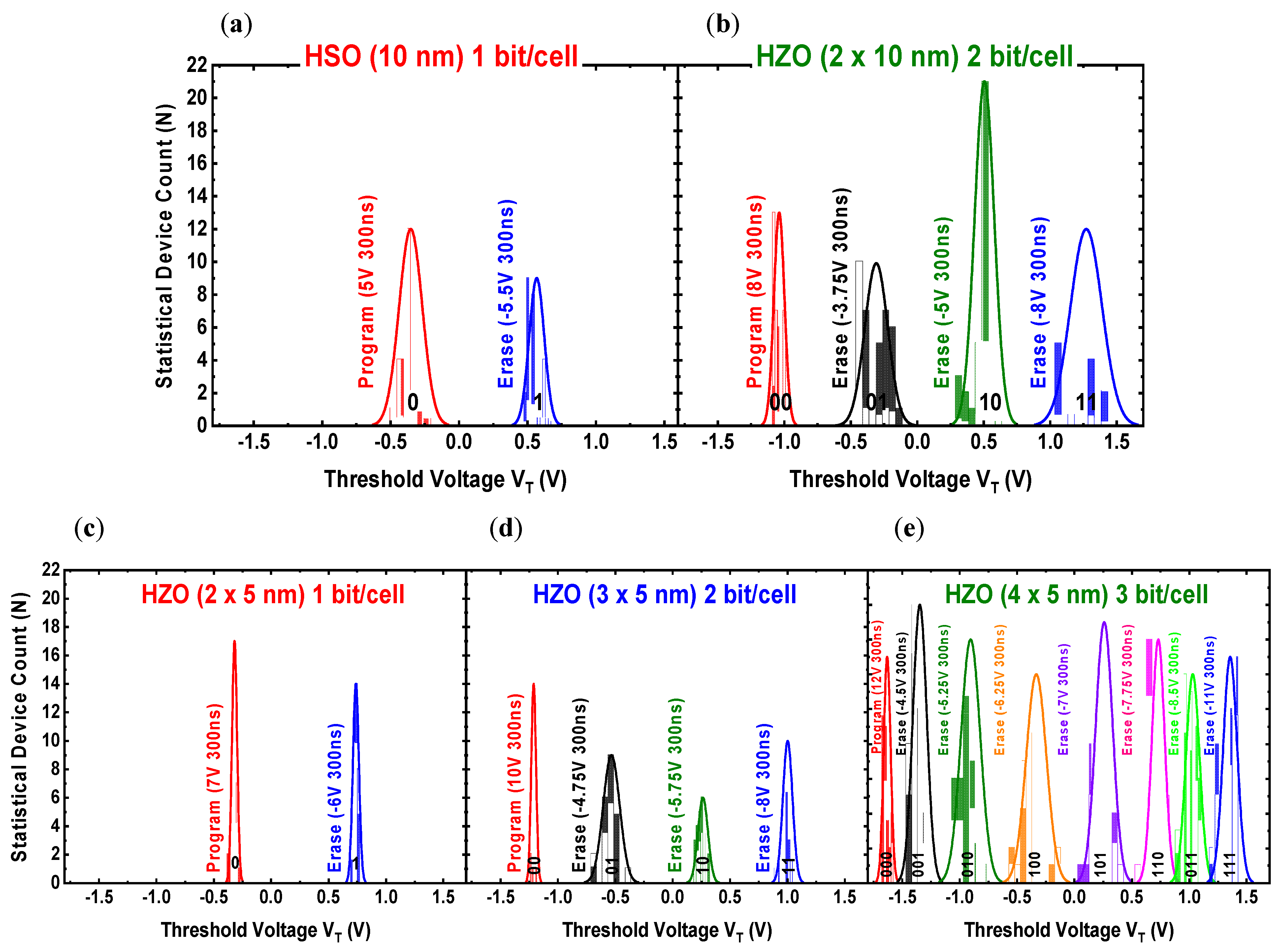
3.3. The Multi-Level Coding Operation (1 bit, 2 bit, 3 bit/cell)
For a higher storage capacity per cell, the quantization of an underlying memory storage mechanism was explored to realize multi-level storage with a distinct separation between the levels. For instance, the charge quantization as in a floating gate or charge trap concept enables a quantized accumulation of stored charges to be mapped to states beyond the single-level cell [
25]. Likewise, the phase-change memory (PCM) relies on the quantization of the resistance change by an induced control of the crystallization level for chalcogenide alloys (GST) [
26]. Practically, both concepts are similarly challenged by the aggressive scalability where noise effects, interference between cells, and statistical fluctuations require error correction coding.
Similarly, the FeFET utilizes the quantization of the ferroelectric polarization switch ing to realize multi-level storage. For different ferroelectric stack thicknesses, the 1–3 bit/cell storage is shown by the V
T distribution to reflect in
Figure 9 the different operating levels. The V
T histogram distribution in
Figure 9 was extracted from the ER V
T shift of
Figure 8 at selected ER amplitudes, as one requirement for reliable MLC storage is the maximized VT shift. In addition, the variability of intermediate states can affect the maximum bit/cell that can be reliably stored. Hence, the single bit/cell operation was reliably stored for the thinner (10 nm) ferroelectric film thickness as in the HSO and HZO-based stacks (
Figure 9 a,c). As the ferroelectric layer thickness is increased with lamination, the storage capacity is extended to a two bit/cell as in
Figure 9b,d, or even as three bit/cell storage (
Figure 9e).
In essence, the MLC operation in
Figure 9 is illustrated for a FeFET based W × L (25 µm × 25 µm) where the intrinsic polycrystalline film variability is minimal. As outlined earlier, a limited V
T shift window was present for the HSO material at the same thickness (20 nm) compared to the HZO. This indicates that the alumina interlayer insertion for the HSO stack caused a deviation from the optimal ferroelectric phase. This is indeed in line with the HSO sensitivity to dopant content concentrations [
27]. Therefore, the optimal tuning content and crystallization properties are different for a ferroelectric laminated stack as compared to a single ferroelectric layer. Thus, the careful control of the HSO doping concentration is crucial for optimum ferroelectric phase stabilization especially in the presence of the alumina interlayer. In contrast, the broad ferroelectric phase window in the HZO material indicated stable ferroelectric properties with lamination, and more particularly in FeFET in the form of a higher MW size.
3.4. The Maximum MW Dependence on Ferroelectric Stack Thickness
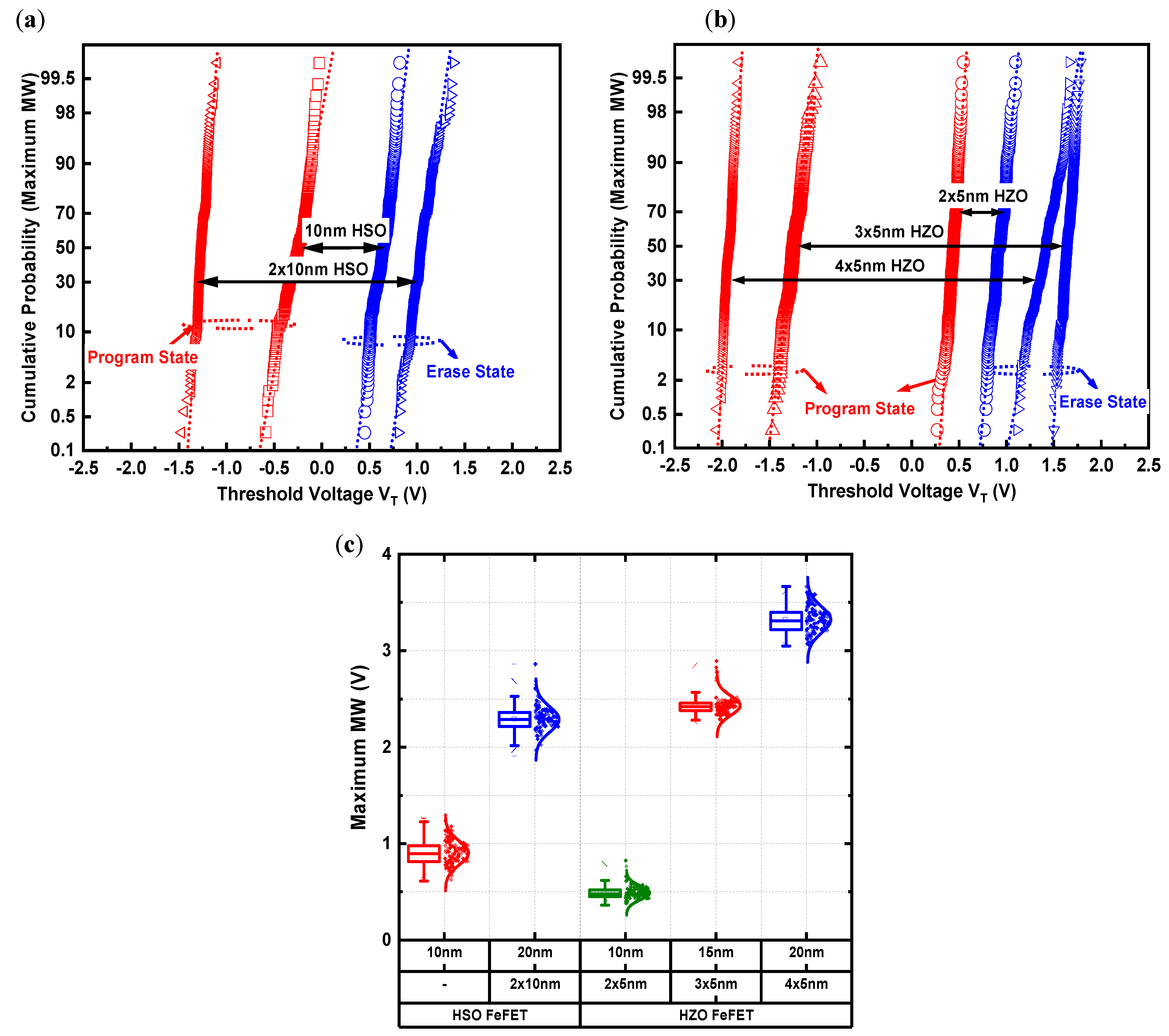
The primary role of the ferroelectric stack lamination is to enable an increased ferroelectric layer thickness without jeopardizing the optimal properties such as the ferroelectric P
r. At a sufficiently high P
r, the linear relation between the ferroelectric stack thickness and the MW increase as in Equation (1) remains intact. This aim of the ferroelectric stack lamination for a maximized MW upon an increase in thickness can be pointed out by the global wafer cumulative probability of the PG/ER V
T shift (
Figure 10a,b) based on the obtained conditions of the saturated switching (
Figure 8). The increase in the MW to values close to the theoretical and maximum values of the MW shown earlier in
Figure 3b indicates significant merits for ferroelectric stack lamination to stabilize the optimal ferroelectric properties at higher film thicknesses.
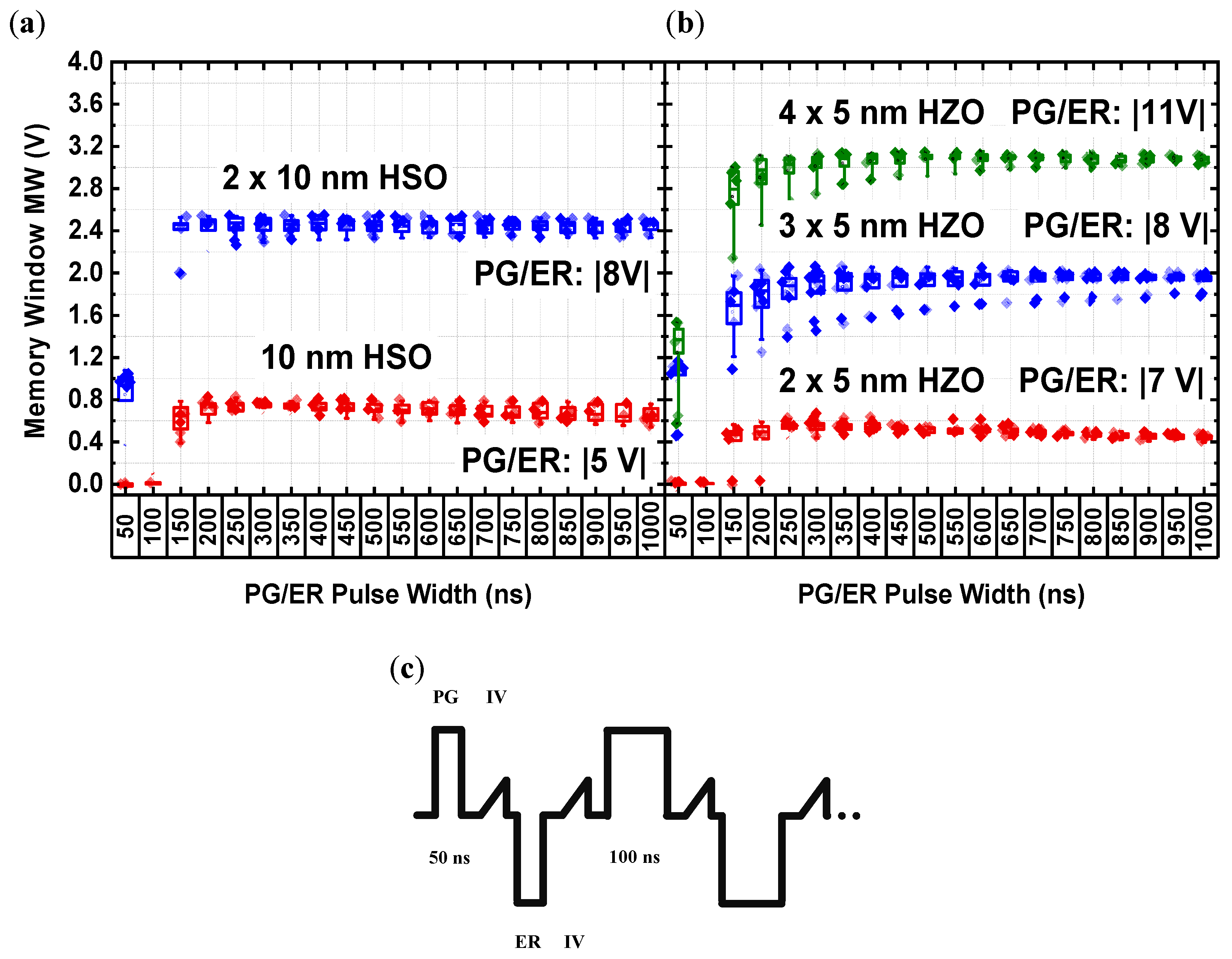
Similarly, the MW in
Figure 11 was measured for each ferroelectric stack thickness at an optimal pulse amplitude while sweeping the PG/ER pulse width (50 ns to 1 µs) was swept.
Figure 11 shows a small MW change beyond the 300 ns pulse width; this indicates a saturated switching at a MW maximum for each thickness. Thus, the field magnitude of switching (
Figure 8) as well as the pulse width sweep (
Figure 11), both show an increasingly higher MW upon the thickness increase indicating a preserved high P
r as a result of the lamination. This trend of MW dependence on the ferroelectric stack thickness is illustrated in
Figure 10c by the plot of the maximum MW versus the ferroelectric stack thickness.
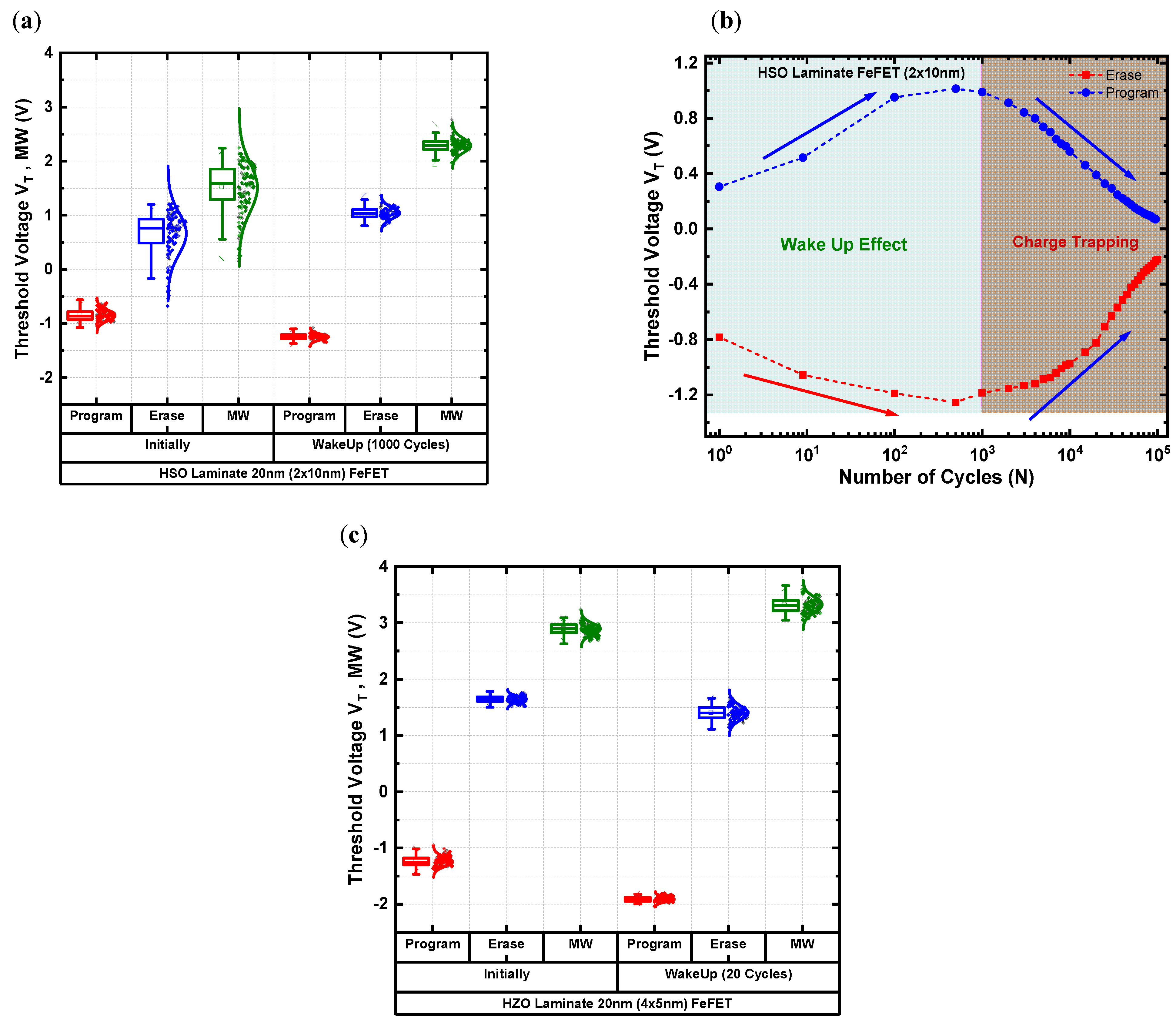
3.5. The Role of Wakeup and Charge Trapping
The initially anticipated effect of the insertion of an alumina interlayer appeared in the optimal ferroelectric P
r and was more critical for the HSO material. However, the further role of the alumina interlayer is important when considering the material phenomenon as a wake-up effect of the HSO and HZO laminates. The HSO global wafer PG/ER V
T and MW distribution as in
Figure 12a measured for FeFET W × L (4 µm × 4 µm) showed a higher switching variability for pristine devices. This variability is due to the different initial phases in the pristine film. The wakeup cycling causes an induced transition to a dominant ferroelectric phase for a narrower V
T and for MW distribution. The post wakeup increase in the MW size indicates a higher post wakeup remnant polarization. This effect was monitored by the V
T evolution over cycling as in
Figure 12b where the symmetric |8 V|, 300 ns pulses showed a gradual and symmetric increase in the PG/ER V
T window to a maximum at 10
3 cycles. This increase in the MW size with the wakeup P
r increase was compensated by a dominant charge trapping effect beyond the 10
3 cycles. This lead to the MW closure.
The trend shown in
Figure 12b reveals two different dominant effects inside the stack for V
T switching as wakeup where a maximized V
T window is obtained versus charge trapping that leads to V
T window closure. In contrast, the wake-up effect in particular was less pronounced in the case of the HZO laminate as shown in
Figure 12c. In the case of the HZO laminates, the maximum MW was reached in a fewer number of wake-up cycles. In contrast to the HSO material, the HZO initial and post wakeup variability were lower. In the context of the multi-level cell operation, both the wakeup and charge trapping effects can practically hinder initial and steady MLC operations. Additionally, as indicated in
Figure 12b, the pre-requirement of wakeup cycles to reach the maximum MW size for reliable MLC operations will in turn limit the maximum enduring range of the device. As indicated in
Figure 12a–c, the wakeup effect is strongly dependent on the material and stack type as well as the thermal budget conditions [
28].
3.6. The MLC FeFET Area Dependence
In a polycrystalline ferroelectric film, the obtained properties result from a superposition effect due to a large ensemble of grain sizes and texture distributions [
29]. In large ferroelectric areas i.e., FeFETs with large feature sizes, the averaging effect produces comparable ferroelectric properties. Thus, a uniform FeFET response with minimal fluctuations in the V
T shift is measurable on a statistical level [
14]. In contrast, the area downscaling features, in particular, the transition to a more discrete distribution of the orientation-dependent coercive field. In turn, the magnitude factor of the surface potential and hence the V
T as well as the MW becomes discrete in distribution and thus raises stronger statistical fluctuations. At ultimate scalability, the discrete type of the distribution of countable grains reduces to a single grain producing further statistical fluctuations. However, a single grain also features just a single, sharp switching transition, also known as instant switching [
30].
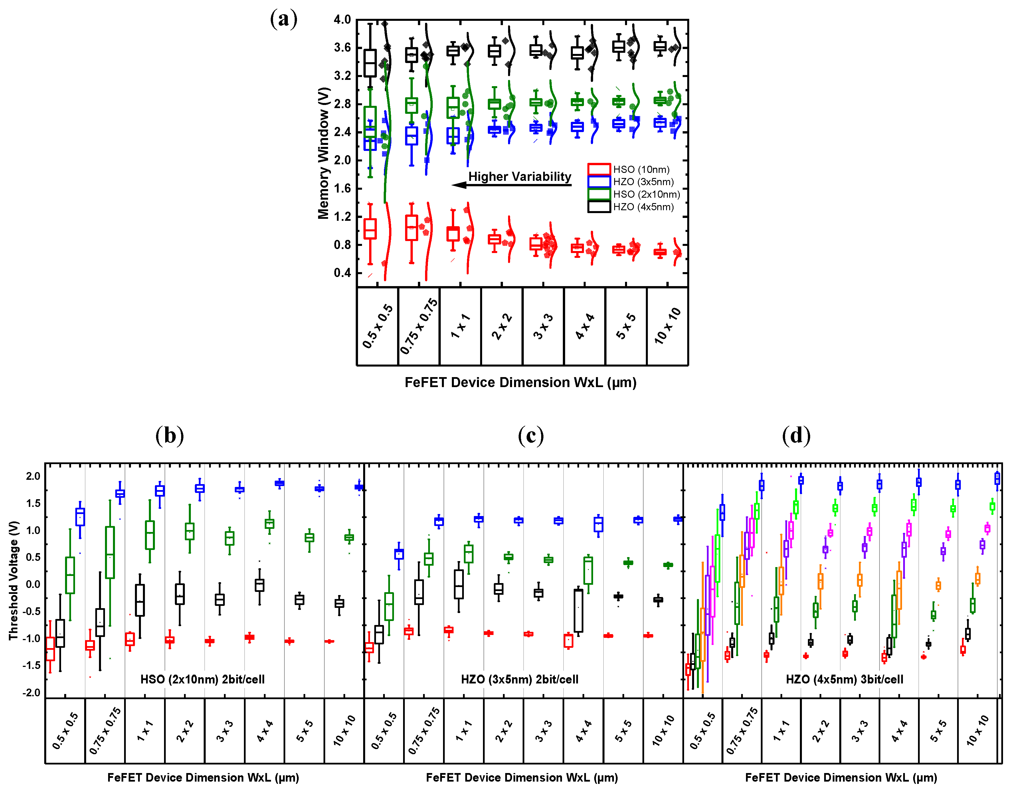
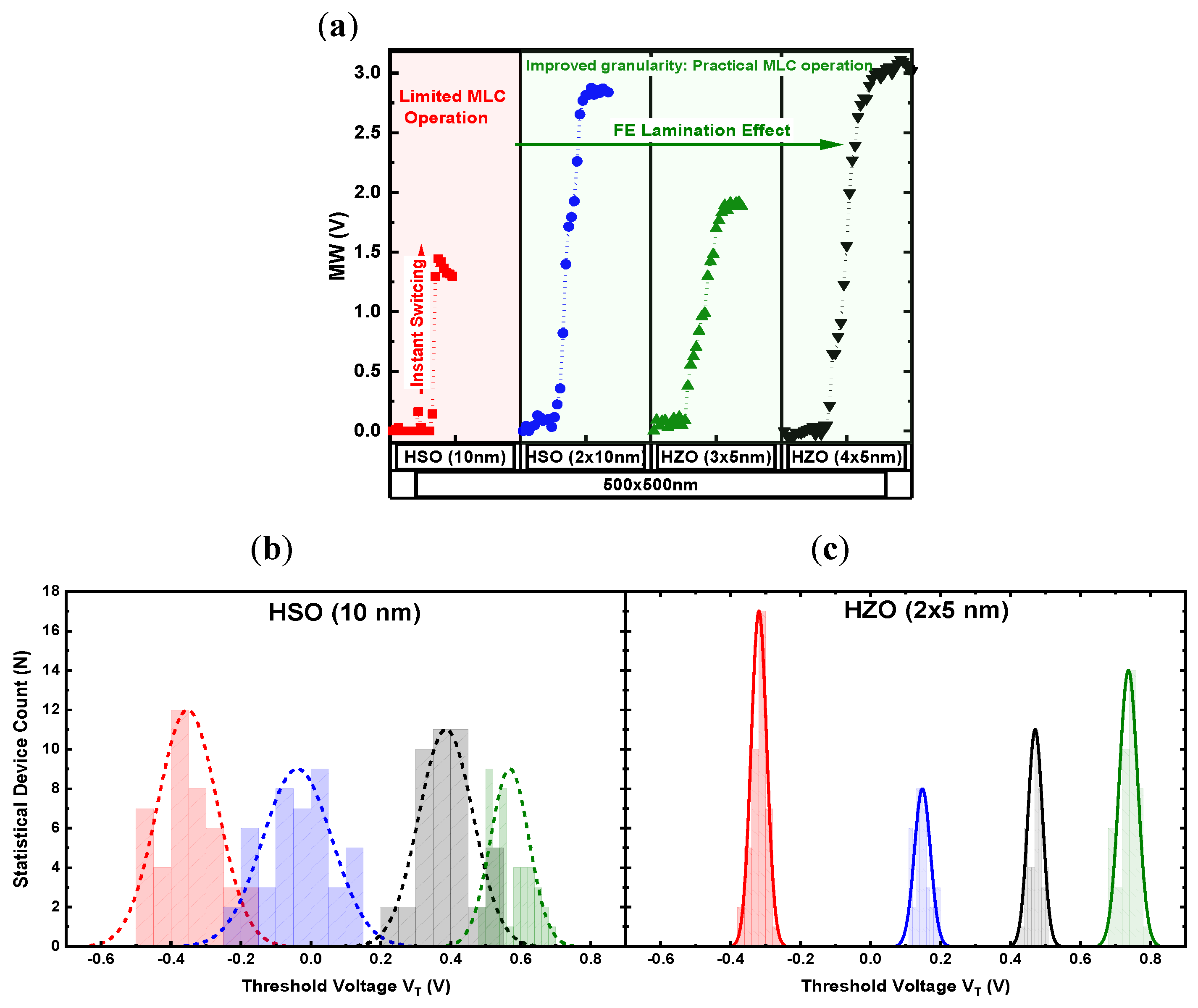
From an MLC operation perspective, the statistical fluctuations as well as the instant switching as features of the ferroelectric area scalability are key challenges for an MLC-based FeFET. An instant switching FeFET has no accompanying intermediate states and is thus impractical for MLC storage. Likewise, statistical fluctuations increase the overlap in distributions and prevent a reliable separation between the MLC states without complex error correction algorithms. Hence, the area dependence of the FeFET variability becomes an important reliability factor especially for the MLC storage. The MW variability versus the area is measured for FeFETs with dimensions in the range from W × L (10 µm × 10 µm) to (0.5 µm × 0.5 µm) of the different HSO and HZO based ferroelectric stacks.
In
Figure 13a, the large FeFETs show a small MW variation and feature a transition toward an increased MW variation as the FeFET area is scaled. As outlined earlier, the high variability affects the MLC storage due to the higher variation in the intermediate levels as shown in
Figure 13b–d for a 2–3 bit/cell operation, particularly with the evolution toward a smaller device area. This size dependent variability is also a strong function of the type of ferroelectric material, stack structure control, and essentially the thermal budget. One of these optimization aspects is achieved by the ferroelectric stack lamination. For the thin ferroelectric layer, the grains exhibit columnar growth between the two electrodes. The stack lamination provides an interruption barrier for the columnar grain growth. In turn, this serves to improve the ferroelectric stack granularity. This enables the gradual switching transition in the form of an increased count of the intermediate storage levels as shown in
Figure 14a. In contrast, the instant switching dominates for the single ferroelectric layer without lamination considering the same W × L (0.5 µm × 0.5 µm) FeFET dimensions. The instant switching reflects a single grain formation where the average grain size growth is dependent on the applied thermal budget to crystalize the film [
20,
26]. Another key merit, as shown in
Figure 14b, is the narrow V
T distribution when the HZO ferroelectric stack is laminated (2 × 5 nm). This enables a reliable 2 bit/cell storage. In contrast, the HSO of the same thickness (10 nm) without lamination showed a broader V
T distribution thereby preventing a reliable 2 bit/cell storage.
3.7. The MLC Retention and Endurance
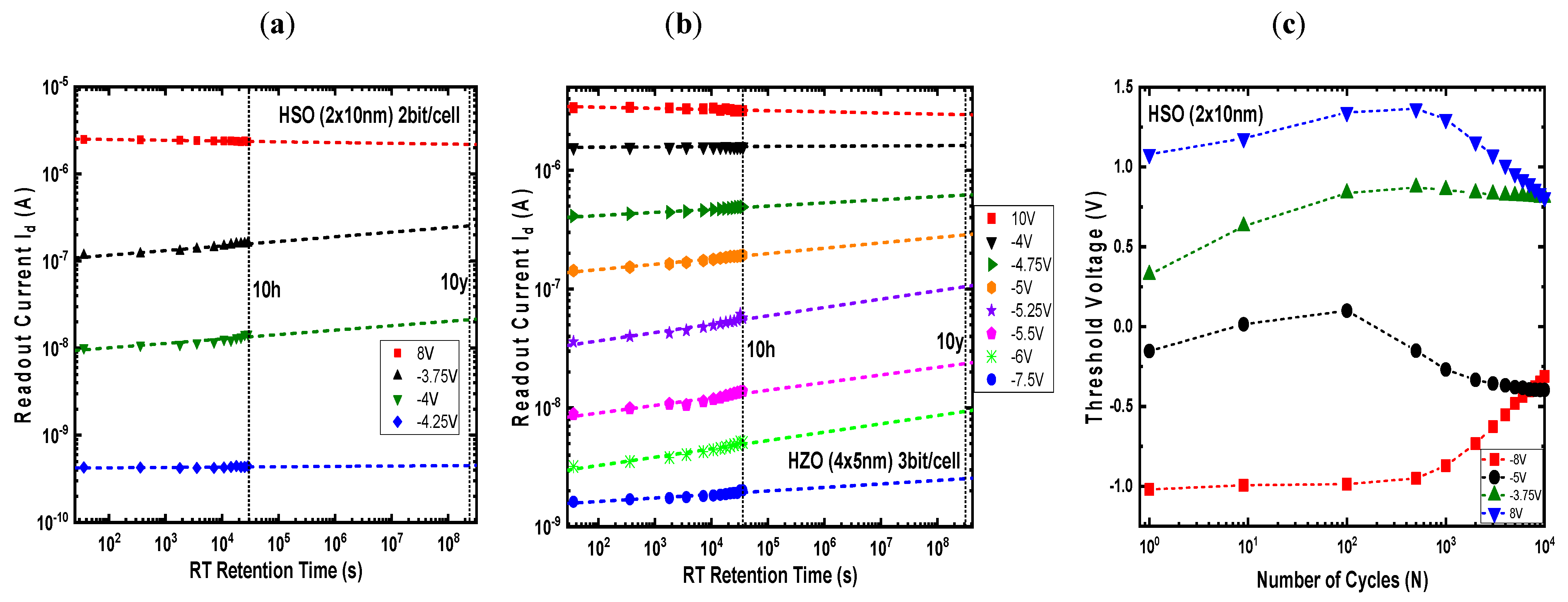
To define the VT shift of each MLC storage level, the FeFET operates partially in a ferroelectric sub-loop switching. At the sub-loop operation, the switchable dipoles have a preferential orientation that favors a low voltage unsaturated switching. However, this has at the same time the net effect of a lower Ec and renders the dipoles more susceptible to reversible switching. Hence, the retention stability of the different VT levels is an important factor of reliable MLC storage. The retention was measured as 2 bit/cell (HSO) and 3 bit/cell (HZO) by initially programming the FeFET and applying ER pulses of different amplitudes per each storage level; the readout current of each state was then monitored for 10 h at room temperature (RT).
Figure 15 shows the MLC retention with a stable evolution of the readout current versus the retention time of each storage level. This was further extrapolated to the 10 years retention time indicating a stable MLC storage. The endurance characteristics of the stored multi-levels is illustrated for a 2 bit/cell operation measured at a 300 ns pulse width at the corresponding four levels of the HSO (2 × 10 nm) ferroelectric stack. The endurance as in
Figure 15 was preceded by initial wakeup cycles to achieve the MW size of an MLC 2 bit/cell storage, and this was followed by the endurance of 10
4 cycles. Initially, the separate 2 bit/cell levels were present up to 10
3 cycles and were reduced for higher cycling ranges due to the charge trapping effects causing a degradation of the lowest and highest V
T levels.
Table 1 gives an overview summary of the laminate FeFET performance in the benchmark with the recent reports on the FeFET concept compared to the Flash and RRAM concepts. The laminate FeFET concept offers a gate stack and a material engineering approach for realizing a multi-level storage solution that can extend the storage density of planar or vertical FeFETs.
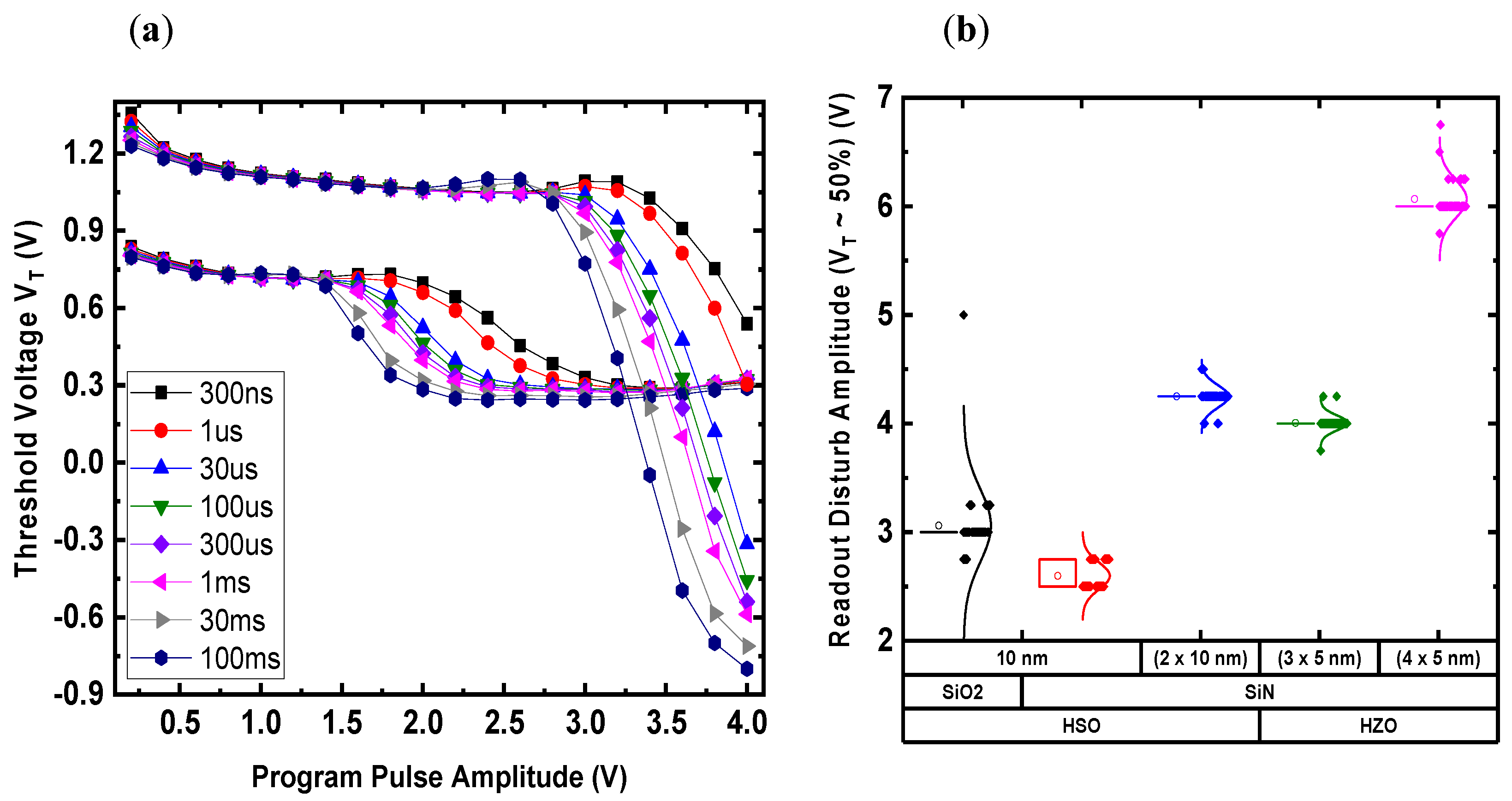
3.8. The Pass Voltage Disturb Effect
The high coercive field in the fluorite structure-based ferroelectrics have several advantages for the FeFET concept, particularly in terms of the maximum MW and the retention reliability. The aggressive ferroelectric thickness scaling renders the net operating voltage (V
c = E
c * d
F) increase, upon a higher coercive field, insignificant when compared to the low coercive field perovskite structure-based ferroelectrics. Another practical consideration for the higher coercive field is the disturbance properties when the FeFET operates in a memory array configuration. The readout of a selected cell relies on the application of the pass voltage (NAND configuration) or the inhibit voltage (AND configuration) of the unselected cells. This pass voltage provokes a cell disturbance that becomes particularly critical for a stored state with an opposite polarity e.g., an ER state under a positive pass/inhibit voltage. Due to the nucleation limited switching (NLS) behavior of the fluorite structure ferroelectrics, the voltage amplitude and time can influence the cell disturbance. This characteristic is explored in
Figure 16a. The ER state was initially written, the positive amplitude was screened at different times (300 ns to 100 ms) and the V
T shift toward the PG state was monitored. The classical tradeoff between the pulse amplitude and the pulse time defines the onset of the V
T shift. The laminate HSO (2 × 10 nm) showed a larger margin for the disturbance free operation compared to the same HSO material with a single 10 nm thickness. For an MFIS-based FeFET, the disturbance characteristic is a function of the interface layer type and the FE stack optimization as shown in
Figure 16b. The disturbance amplitude was extracted for the onset of the 50% V
T shift (ER to PG transition). For the same FE material (HSO at 10 nm), the SiO
2 IL showed a disturbance voltage that was higher compared to the SiN in line with the higher permittivity effect for the case of SiN, i.e., a higher field was present across the ferroelectric layer. The stack lamination for the same SiN-based interface layer shows higher pass disturbance voltages. For the same total ferroelectric layer thickness (20 nm), the increase in the number of lamination layers in HZO (4 × 5 nm) gave a higher voltage margin of the disturbance compared to the HSO (2 × 10 nm). The stack lamination is a tuning knob that represents tradeoffs between the increased pass/inhibit voltage disturbance margin, the operating voltage increase, and variability reduction.
3.9. The Laminate FeFET-Based Synaptic Device
In biological neuro-synaptic behavior, the neurotransmitters that are released by a pre-synaptic neuron bind to the receptors of a post-synaptic neuron to modulate the flow of ions and thus the membrane potential of the post-synaptic neuron. In an excitatory/inhibitory (E/I) post-synaptic potential (PSP) process, the flow of ions generates net positive/negative charges and results in an increased/decreased membrane potential, respectively. In the simplest form, a neuron produces an output spike as the membrane potential reaches a pre-defined firing threshold potential. Although this may reflect rather deterministic behavior, the neurons can also respond in a stochastic way with a probability of a firing event, increasing with the input stimulus [
34].
This particular feature of stochastic firing can be emulated by the scalable FeFET concept due to the instant and also stochastic switching behavior at the ultimate area scalability [
18]. At the scaled area, a single grain controls the FeFET V
T where a saturated switching occurs once the threshold switching field is reached. Hence, an optimization of the FeFET considers, at the same area, a rather reduced grain count inside the ferroelectric film as well as an increased grain size to achieve the spiking-based instant switching. Practically, the FeFET scaling trend produces dimension ranges that are smaller than the achieved grain size of a ferroelectric film. However, the critical upper dimension at which the instant switching could dominate remains strongly dependent on the process optimization especially in terms of the thermal budget where the grain growth is affected [
20].
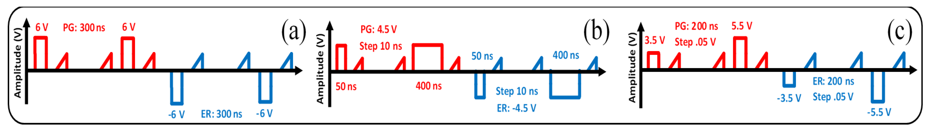
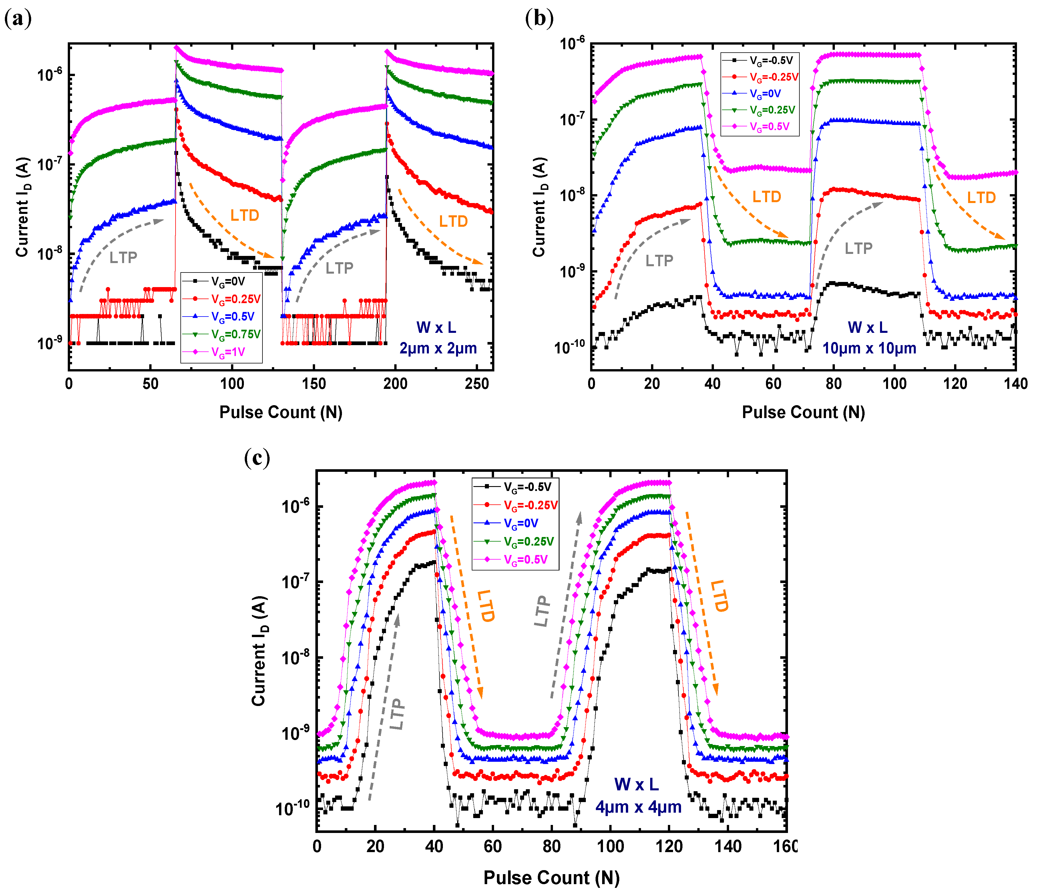
In strong contrast to that aim of emulating the neuron behavior, the synaptic weight storage relies on a fine modulation of the switching polarization to achieve a controlled multi-level weight update. As opposed to the spiking-based FeFETs, the optimization for multi-level storage relies on an increased grain count and a broader texture distribution, which is partially achieved by the ferroelectric lamination. The long-term synaptic potentiation/depression (LTP/LTD) was studied for the ferroelectric HSO laminate stack (2 × 10 nm) using three different test schemes [
35] as depicted in
Figure 17a–c. The synaptic weight update as the current I
D versus the pulse count was plotted in
Figure 18a–c for each sequence and at different set points of the V
G readout. The measurement sequence of the LTP/LTD emulation was applied twice for the reproducible current trend.
In the first sequence, a PG/ER pulse train using an amplitude of |6 V|, 300 ns was applied. This condition was lower than the one used for the saturated switching. Based on the accumulative switching behavior of the ferroelectric materials, the LTP/LTD as shown in
Figure 18a reflected a V
T decrease/increase, and thus produced an increase/decrease in the current, respectively. The LTP/LTD can similarly be achieved using the second sequence (
Figure 17b) where the pulse width sweep (50 ns to 400 ns) at a constant amplitude |4.5 V| was used to modulate the current as shown in
Figure 18b. A similarity in the trends of
Figure 18b is related to the dynamic range of current modulation as well as the current magnitude in relation to the set point of the V
G readout. An increase in the V
G readout shows a systematic shift of the full LTP/LTD curves toward higher current values. Likewise, the dynamic range of the current modulation decreased as the V
G readout increased. Both the LTP/LTD trends in
Figure 18b reflect a narrow FeFET switching window as per the LTP/LTD pulse conditions applied where a limited field has unsaturated ferroelectric switching, as is visible in the limited maximum of the dynamic current range.
As the third sequence, the pulse amplitude sweep was used in
Figure 17c at a constant pulse width (200 ns) to capture the full window of the LTP/LTD as shown in
Figure 18c for the different V
G readout. The fine increase in the amplitude generated an increased number of levels with approximately three orders of magnitude current change, and the effective increase in levels with the amplitude was consistent with the ferroelectric stack lamination. Although the second and third sequences of LTP/LTD in
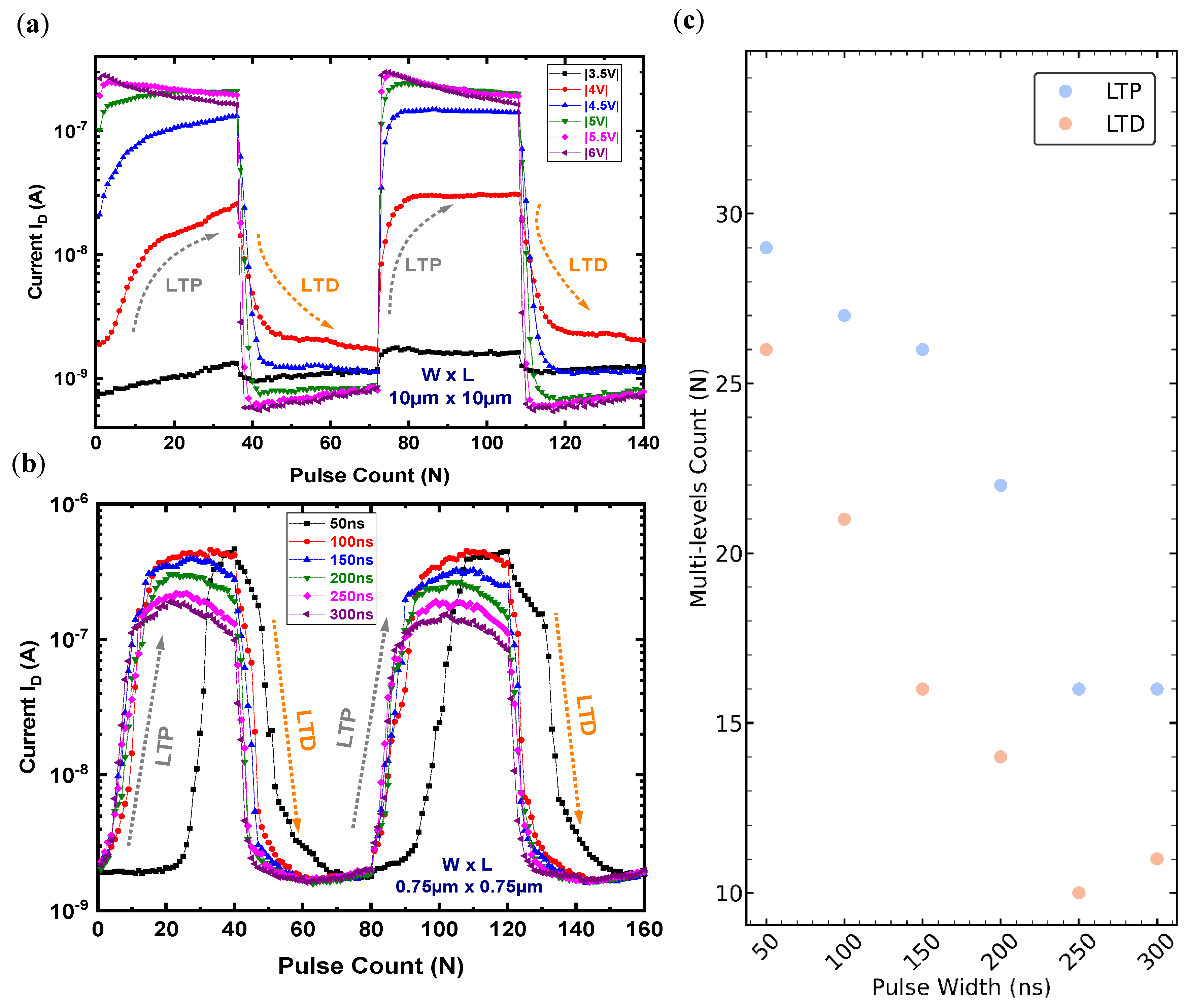
Figure 18b,c were studied at a constant selected pulse amplitude (|4.5 V|) or pulse width (200 ns), the impact of different amplitudes or pulse widths can be illustrated in
Figure 19a,b for each sequence, respectively. For the second sequence, the pulse amplitude sweep had, as was outlined earlier, an increase in the current dynamic range as the amplitude increases (e.g., |4 V|, |4.5 V|) shown in
Figure 19a. At higher amplitudes such as |6 V|, a decrease in the saturation current reflects a dominant charge trapping effect that prevails over the saturated ferroelectric switching. Although to a lesser extent, a similar effect was present for the third sequence at the different values of the constant pulse width (50 ns to 300 ns) in
Figure 19b. Importantly, at a shorter pulse width such as 50 ns, a higher amplitude and hence a higher pulse count was needed to cause a current modulation i.e., ferroelectric switching. This is due to the tradeoff between the field and time-dependent ferroelectric switching [
36]. Hence, the LTP/LTD curve of the 50 ns pulse width was relatively shifted in
Figure 19b to a higher pulse count.
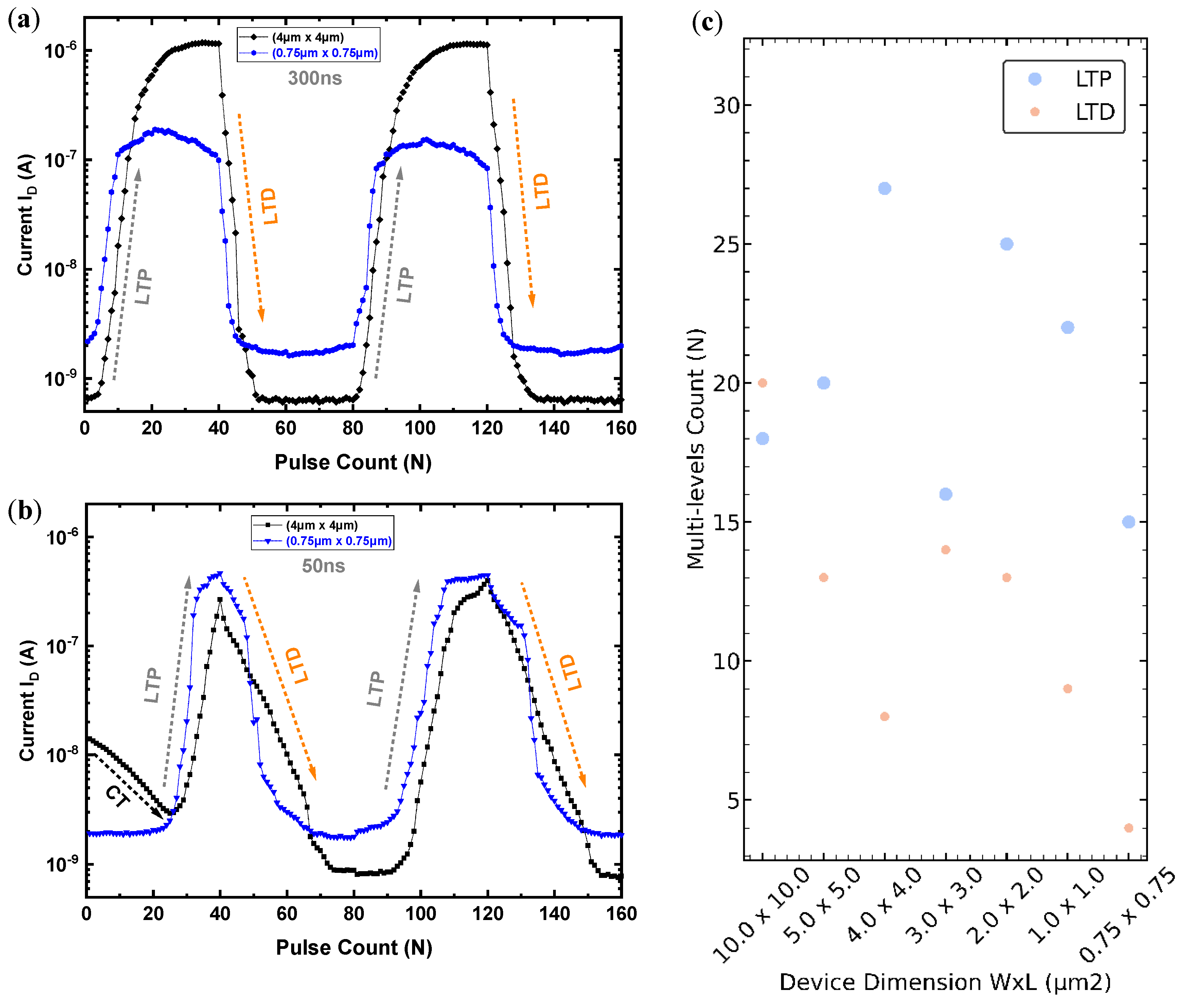
Although the higher pulse width (>50 ns) appears indifferent in the LTP/LTD trend of
Figure 19b, an extraction of the multi-level count gives a rather valuable insight. The multi-levels were counted at 1 nA search resolution of the second LTP/LTD cycle while excluding the low and high current saturation ranges (
Figure 19b). The impact of varying the write pulse width of the third sequence is shown in
Figure 19c where the maximum number of achieved levels is inversely proportional to the pulse width. At the 50 ns pulse width, the multi-level count was at a maximum and decreased toward the 300 ns conditions. This reveals that the sequence type, pulse amplitude, and pulse width conditions have different switching dynamics of the ferroelectric material and ultimately affect the LTP/LTD response shape as well as the multi-level count.
Additionally, the LTP/LTD multi-levels count was proportional to the area as in
Figure 20c with the dimension sweep from (10 µm × 10 µm) to (0.75 µm × 0.75 µm) indicating a decrease in the multi-levels count. The impact of the pulse width and the area can be further summarized in
Figure 20a,b by the comparison of selected devices (4 µm × 4 µm) versus (0.75 µm × 0.75 µm) at the 50 ns and 300 ns pulse width conditions. Although the multi-levels count declined as the area shrank, the clear advantage of the ferroelectric stack lamination appears in the actual presence of these intermediate levels in comparison to the instant switching behavior as indicated earlier in
Figure 14a. This one aspect of ferroelectric stack optimization indicates the possible variability reduction in scaled FeFET devices.
3.10. The Laminate FeFET Based Synaptic Metrics
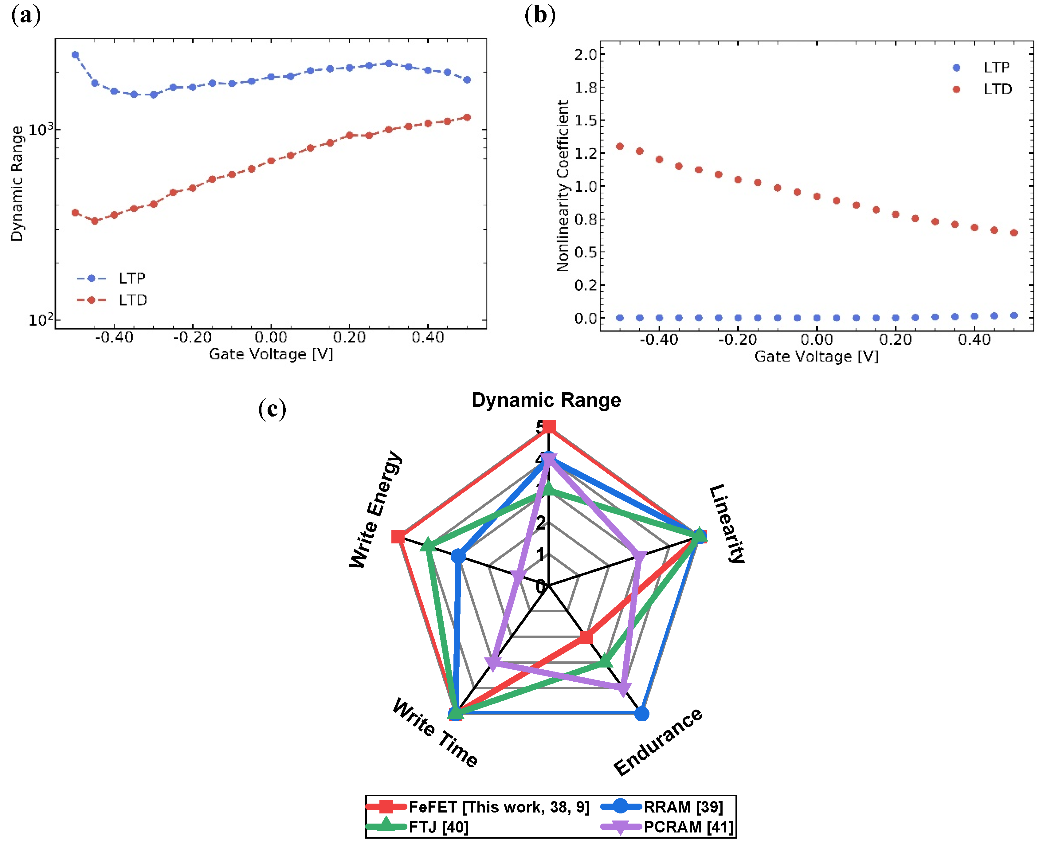
An optimal electronic synapse is characterized by certain performance criteria. These are stated in terms of the LTP/LTD maximum dynamic range (DR) and nonlinearity coefficients. An ideal synapse has extremely linear and symmetric LTP/LTD responses at maximized I
on to I
off current ratios i.e., the weight update covers a wide DR. The FeFET synaptic LTP/LTD can be characterized based on a fitting model as proposed by Yu et al. for extracting the nonlinearity coefficient α [
37]. For a FeFET-based synapse, the DR and nonlinearity becomes a function of the readout voltage as shown in
Figure 21a,b. The DR and nonlinearity coefficients were extracted from the synaptic LTP/LTD that was measured using the amplitude-based sequence as shown earlier in
Figure 18c. The DR was extracted as the weight ratio between the LTP/LTD current measured after the first and final pulse of the sequence in
Figure 17c. The LTP showed a higher DR compared to the LTD one in the current transition in
Figure 18c. For a symmetric synaptic response, the DR becomes equal for the LTP/LTD operation. The LTP in
Figure 21b shows excellent linearity whereas in the LTD case, the linearity improves as the readout voltage increases. The linearity coefficient dependence on the readout voltage is directly linked to the different operation regime of the FeFET I
D–V
G. For a higher readout voltage, the improved linearity reflects a gradual response at an even current I
D–V
G shift for the ER pulse amplitude increase. The FeFET concept [
9,
38] is compared in
Figure 21c with other technologies [
39,
40,
41]. The high dynamic range, low energy, and linearity are among the key merits of using the FeFET as a synaptic device.


 ,
, 


