Article

Batteryless Electronic System Printed on Glass Substrate

1
RISE Research Institutes of Sweden, Digital Systems, Smart Hardware, Printed, Bio- and Organic Electronics, Bredgatan 33, Box 787, SE-60117 Norrköping, Sweden
2
J2 Holding AB, Sjögestad Rosendal, SE-58392 Vikingstad, Sweden
3
RISE Research Institutes of Sweden, Built Environment, Building and Real Estate, Glass, Vejdes Plats 3, SE-35252 Växjö, Sweden
*
Author to whom correspondence should be addressed.
Electron. Mater. 2021, 2(4), 527-535; https://doi.org/10.3390/electronicmat2040037
Submission received: 16 September 2021 / Revised: 4 October 2021 / Accepted: 19 October 2021 / Published: 3 November 2021
(This article belongs to the Special Issue Feature Papers of Electronic Materials)

Abstract

:
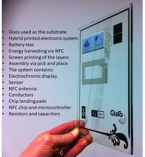
Batteryless hybrid printed electronic systems manufactured on glass substrates are reported. The electronic system contains a sensor capable of detecting water, an electrochromic display, conductors, a silicon chip providing the power supply through energy harvesting of electromagnetic radiation, and a silicon-based microcontroller responsible for monitoring the sensor status and the subsequent update of the corresponding display segment. The silicon-based components were assembled on the glass substrate by using a pick and place equipment, while the remainder of the system was manufactured by screen printing. Many printed electronic components, often relying on organic materials, are sensitive to variations in environmental conditions, and the reported system paves the way for the creation of electronic sensor platforms on glass substrates for utilization in see-through applications in harsh conditions. Additionally, this generic hybrid printed electronic sensor system also demonstrates the ability to enable autonomous operation through energy harvesting in future smart window applications.

Graphical Abstract

1. Introduction

A tremendous amount of effort has been, and is being, spent on developing electronic components and systems based on organic active materials. Such organic-based materials can be processed from solution, thereby allowing for manufacture by printing on flexible substrates, such as paper, textiles and plastic [1,2,3,4,5]. These research activities have several objectives; to cut production costs and to allow for new form factors of the resulting devices are two examples.
However, organic molecules and polymers are usually sensitive to the environmental conditions of their surroundings. Degradation of materials and devices may occur due to photooxidation and/or fluctuations in temperature and humidity. This is well known in, for example, organic photovoltaic devices and organic light-emitting diodes, and proper encapsulation is required in order to achieve reliable device functionality over a long time in various environmental conditions [6,7,8]. Therefore, printed electronic components manufactured on, e.g., paper or plastic substrates are in general very sensitive to environmental fluctuations due to the inherently weak barrier properties of these substrates. This may be solved by lamination of the device between two barrier films, for example, a plastic film which includes a thin metal oxide coating. However, this adds expense to the manufacturing process, both in terms of material costs and for the additional processing steps.
Glass belongs to a class of materials that exhibit excellent barrier properties, and another option would therefore be to protect printed electronic devices against the environment by lamination between glass sheets [9,10]. The water vapor transmission rate (WVTR) and oxygen transmission rate (OTR) properties of glass are extremely low, thereby ensuring hermetic sealing upon device encapsulation between glass sheets. This is of critical importance for printed electronic components relying on organic materials, to prevent ingress/egress of moisture and oxygen.
The use of glass lamination to mitigate humidity dependence in screen printed electrochromic displays has already been reported [11]. Standard lamination methods used by glass window manufacturers were used to encapsulate the electrochromic displays, and thereby circumvent the humidity dependence. For the present study, the development activities are instead focused on the manufacturing of a complete electronic system by means of screen printing directly on top of a glass substrate. The outcomes prove that a variety of materials, including insulators, semiconductors and conductors, can be deposited onto glass. The substrate transparency allows for various see-through applications, e.g., electronic displays.
Glass is becoming ever more important as a building block in architectural buildings, and this is also a strong motivation to add electronic functionalities to the glass itself. There are many applications in which electronic functionality could add value to the glass. Electrochromic smart windows are perhaps the most well-known application when it comes to adding electronic functionality to glass [12]. Such electrochromic films are typically manufactured by either coating the functional layers directly onto the glass, or by pre-manufacturing the electrochromic film on, e.g., a plastic or thin glass sheet that is subsequently laminated onto the glass pane of the window. Many other kinds of electronic conductors [13], components and systems will evolve in the future, either by implementation directly onto glass substrates or by laminating the printed electronics between glass sheets. Examples of such printed electronic components include solar cells [14], displays [15] and transistors [16], the first two of which also require the transparency of the substrate. Another feasible application, also taking advantage of the barrier properties of glass, would be to add electronic functionalities on both sides of the glass sheet. Such circuitry would enable, for example, utilization of a sensor device located on one side of the glass substrate, while the other part of the system is located on the opposite side of the glass substrate. This would even allow for monitoring of various parameters in harsh conditions, e.g., toxic, corroding, etc., because the sensor would be the only component that is exposed to the harsh environment, with the remainder of the electronic circuitry safely located on the other side of the glass substrate, or safely laminated between two glass sheets. In such a system, the electronic connection between the two sides of the glass substrate could be established wirelessly, e.g., through capacitive coupling, or by the 3D printing of conductors around the edges of the glass.
In addition to this, glass sheets can be produced in a large range of thicknesses. Standard glass used in windows is typically a few millimeters thick, but both thicker and thinner glass sheets exist, depending on the application. Thin glass sheets in the range 50–100 µm also exist, allowing for curvature and even roll-to-roll manufacturing [17,18]. Therefore, from a manufacturing perspective, there are plenty of manufacturing methods that can be chosen for the materials’ deposition, and sheet-to-sheet screen printing was chosen for the manufacturing of the components and systems presented herein.
We demonstrate that an electronic system containing an electrochromic display, along with other kinds of electronic devices and circuity, can be printed directly on top of the glass substrate in order to take advantage of the transparency of glass. Additionally, the resulting electronic system is a so-called hybrid electronics system, which combines electronic components and sub-systems based on both inorganic (silicon) and organic polymer materials. The silicon chips, and other traditional passive components, such as resistors and capacitors, are assembled onto the glass using pick-and-place equipment. Silicon-based electronics are utilized to provide communication and efficient energy harvesting, while advantage is taken of the organic materials in components requiring a large area and thinness. The batteryless system is activated and powered through the NFC interface of a mobile phone. The NFC chip provides sufficiently high voltage to initialize an adjacent microcontroller, which monitors the status of a sensor and subsequently updates the electrochromic display. Firstly, the microcontroller checks the status of the sensor, which in this case is a very simple water sensor that is triggered by water droplets short-circuiting the adjacently positioned sensor electrodes. Depending on the status of the sensor, the microcontroller then activates the electrochromic display segment that corresponds to the sensor status. Both the sensor and the electrochromic display, as well as the interconnects, contact pads for the silicon chips and the NFC antenna are screen printed directly on top of the glass substrate.
The demonstration model presented herein shows that it is possible to manufacture various kinds of electronic components, conductors, contact pads and antennas by screen printing, as well as to assemble passive components and silicon chips directly onto a glass substrate using pick-and-place equipment. This combination allows for the creation of various kinds of hybrid electronic systems printed directly onto glass surfaces, where autonomous system operation is enabled through energy harvesting solutions: features that are considered both critical and advantageous in the development of emerging smart windows that include additional electronic functionalities in the future.

2. Materials and Methods

2.1. Device Manufacturing

All materials were deposited by a flatbed, sheet-fed, screen printing machine (DEK Horizon 03iX, ASM Assembly Systems, Sollentuna, Sweden) on top of standard float glass substrates (4 mm thick, ~A5 area). The screen-printing tools were based on a standard polyester mesh. PEDOT:PSS (Clevios S V3, purchased from Heraeus, Leverkusen, Germany) was screen printed as the color-changing electrode of the electrochromic display, followed by thermal curing at 120 °C for 5 min in a hot-air conveyor belt oven. An insulator (Ultragraph UVAR, purchased from Marabu, Malmö, Sweden) was then screen printed to define the shape of each electrochromic segment. An electrolyte (VV003, provided by RISE, Norrköping, Sweden) layer was subsequently screen printed into the openings of the insulating layer. The insulating layer and the electrolyte layer were both UV-cured. The electrochromic display was completed by screen printing a carbon-based (7102, purchased from DuPont, Bristol, UK) counter electrode covering the electrolyte. The carbon electrodes of the sensor were screen printed in the same processing step. The carbon ink was thermally cured at 120 °C for 5 min in a hot-air conveyor belt oven. Contact pads, chip landing pads, conducting wires and the NFC antenna were all screen printed from a silver ink (Ag 5000, purchased from DuPont). Wire crossings were created by printing an insulating layer (5018, purchased from DuPont) at those locations, followed by the printing of silver bridges. The silver layers were thermally cured at 120 °C for 5 min in a hot-air conveyor belt oven.
Silicon-based electronic components (microcontroller, energy harvesting chip, resistors and capacitors) were assembled using a pick-and-place machine from Datacon, and the attachment of these components was secured by deposition and the thermal curing of an anisotropic conducting glue. Both the microcontroller (PIC24F16KA101, purchased from Microchip, Chandler, AZ, USA) and the energy harvesting chip (NT3H1101W0FHK, purchased from NXP, Eindhoven, The Netherlands) were used as QFN packages with the dimensions 5 mm × 5 mm × 0.9 mm and 1.6 mm × 1.6 mm × 0.5 mm, respectively. 0603 SMD packages, i.e., 1.5 mm × 0.8 mm, were used for resistors and capacitors.

2.2. Device Characterization

Measurements and demonstrations were carried out at a temperature of ~20 °C and at a relative humidity of ~45% RH. The current vs. time measurements to characterize the switching behavior of the electrochromic display segments and the sensor were performed by using a semiconductor parameter analyzer (HP/Agilent 4155B). To demonstrate the complete system, the required energy was provided through the NFC interface of a mobile phone.

3. Results and Discussion

3.1. Design and Manufacturing of the System

The printed electronic system presented herein was manufactured according to a layer-by-layer screen printing approach, eventually completed by pick-and-place assembly of the silicon-based electronic components onto already printed silver-based contact pads and chip landing pads. A total of seven screen printing steps are required to obtain the targeted architecture of the hybrid electronic system manufactured on glass substrates. For simplicity, only a few of these layers are shown in Figure 1a. The dimensions of the layout measure approximately 11 cm × 9 cm.
No particular optimization of the screen printed NFC antenna was required. The antenna layout shown in Figure 1a enabled energy harvesting via the NFC interface of a mobile phone, upon bringing the mobile phone in close proximity to the antenna structure. It was possible to activate the energy-harvesting chip from both sides of the glass substrate, i.e., within a few centimeters above or below the antenna of the printed electronic system. Hence, the approach of using NFC for energy harvesting purposes is considered reliable. This is also shown in Figure 1b and Video S1 in the Supplementary Materials, where the voltage output level from the energy harvesting chip equals 3 V as long as the mobile phone is kept in close proximity to the NFC antenna. The stable voltage level generated at the output of the energy harvesting chip ensures reliable operation of the complete system; the voltage level of 3 V is subsequently used to operate the microcontroller that, in turn, is responsible for the sensor monitoring and the update of the electrochromic “rain” and “sun” display segments.
The novelty presented herein is that the electronic system is screen printed directly on top of rigid glass substrates, and an evaluation of the adhesion of the most critical printed layers was therefore performed via cross-cut tape tests [19]. Cross-cuts were made in the area of each material printed on glass to be tested. A piece of tape was attached to the relevant cross-cut area, and after some time the tape was rapidly removed. The adhesion was classified by the percent of the printed layer that was removed by the cross-cut tape test. PEDOT:PSS adhered very well to the glass substrate: it received a classification of 4B (less than 5% was removed). The chosen silver ink showed relatively good adhesion: this layer was classified as 3B (5–15% of the printed silver area was removed). The carbon ink, on the contrary, adhered poorly to the glass substrate, as manifested in the fact that a large portion of the printed carbon layer was removed in the cross-cut tape test: it was classified as 1B (35–65% of the printed carbon layer was removed). This could potentially become an issue in future applications, and further development and optimization should be performed to extend the lifetime of the system. However, the adhesion was considered sufficient for the purposes of demonstrating the system, and the addition of water on top of the carbon-based sensor electrodes did not cause any delamination or cracks in the deposited carbon layers.

3.2. Sensor Device

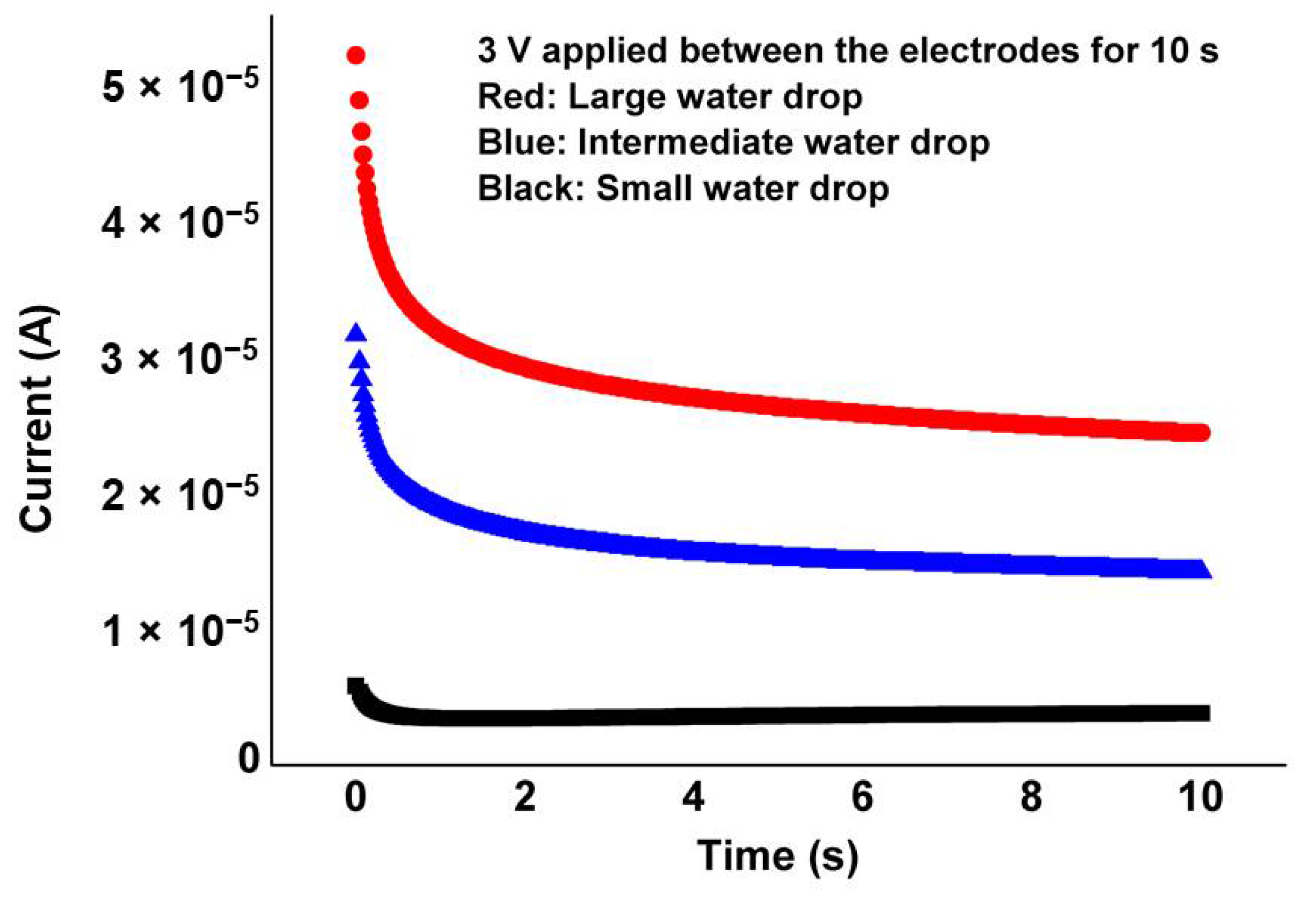
The sensor device used in this system only returns a binary value, the microcontroller simply monitors whether any current is flowing between the two carbon-based sensor electrodes. A water droplet bridging the two electrodes will inevitably cause a current to flow between the two electrodes, due to the fact that the electrodes are supplied with a voltage difference of 3 V from the microcontroller. The current flow relies on ionic impurities in the water as well as water-splitting reactions at the sensor electrodes. If this current level exceeds the predetermined threshold level in the microcontroller, the sensor is in its ON state. The OFF state of the sensor is obtained when no water is bridging the sensor electrodes, i.e., the current flow between the electrodes is disabled. By instead using several threshold levels in the microcontroller, it would be possible to generate an arbitrary number of discrete sensor levels, which in turn would give an indication of the amount of water in contact with the sensor electrodes. This is exemplified by the graphs in Figure 2, showing the effects of water droplets of various volumes on current. The capacitive contributions, observed during the first few seconds, as well as the stabilized current levels, observed during the remainder of the measurement, are both dependent on the area of the carbon electrodes in contact with water. The OFF state of the sensor is omitted in this graph, since no current flow occurs without the water bridge.

3.3. Electrochromic Display

The electrochromic display architecture utilized here was originally developed by RISE, formerly known as Acreo, for the manufacturing of flexible displays on plastic substrates [20]. However, herein we demonstrate the screen printing of electrochromic displays directly on glass substrates for the first time. The screen printed electrochromic display technology exhibits a few unique features. Firstly, all layers were deposited via screen printing, which ensures an efficient approach for low-cost and high-volume manufacturing, either sheet-to-sheet or roll-to-roll. In addition to this, the conducting polymer poly(3,4-ethylenedioxythiophene):poly(styrene sulfonate) (PEDOT:PSS) was used for the color changing electrodes in the electrochromic displays. The material, which is commercially available in many different ink formulations, is intrinsically oxidized to an electronically conducting state. This is an important material property that obviates the requirement of transparent conductive oxide coatings in the electrochromic display architecture (e.g., indium tin oxide, ITO). Furthermore, an electrolyte was used to bridge the electrochromic electrode and the counter electrode; a device architecture that ensures low-voltage operation, which is an extremely important feature in systems powered by energy harvesting. Here, the voltage level of 3 V that was generated at the output of the energy harvesting chip was clearly sufficient to establish full color contrast switching of the electrochromic rain and sun display segments.
The PEDOT:PSS material switches between blue and transparent in its reduced and oxidized state, respectively. An opaque white electrolyte was used to hide the carbon-based counter electrode, hence, the ON (reduced) and OFF (oxidized) states of the electrochromic display segments exhibited a blue and white color, respectively. Once a segment is switched to a certain color state, the color is maintained for a limited amount of time (~15 min in normal environmental conditions) if kept in open-circuit mode. This type of semi-bistable property is yet another advantage of this display technology, since it lowers the total energy consumption, as well as extending the operational lifetime by lowering the voltage strain.
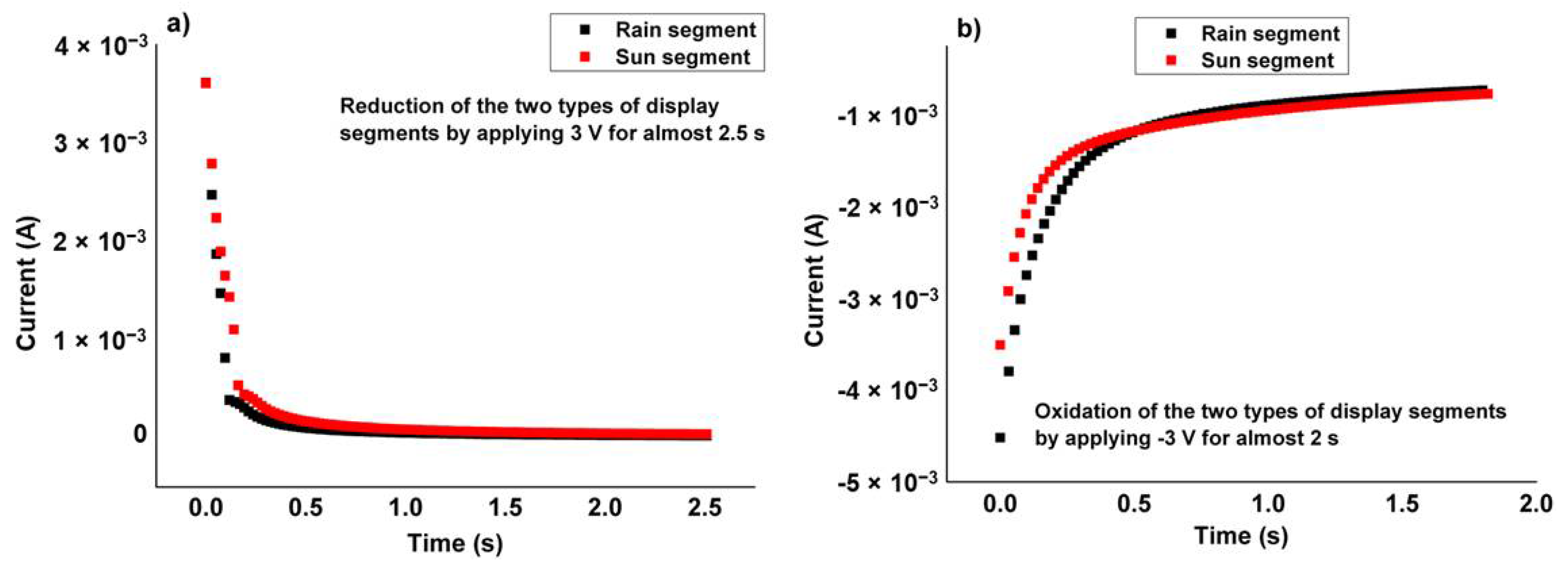
Figure 3 shows the current vs. time characteristics when either reducing or oxidizing the electrochromic segments. Reduction was obtained by applying 3 V to the counter electrode, while the opposite voltage polarity was used to oxidize the segments. The switching time is easier to determine upon reduction of PEDOT:PSS to its semiconducting state, as indicated by the sharp transitions in the current vs. time graphs shown in Figure 3a. At such a transition, the electrochromic PEDOT:PSS-based electrode in contact with the electrolyte is fully reduced, hence also semiconducting, and no further coloration occurs. The coloration from white to blue occurs within ~120 ms and ~160 ms for the rain and sun segments, respectively. Integration of the data in the graphs with respect to these switching times yields the amount of charge required for each switching event. The rain and sun segments require ~200 µC and ~300 µC, respectively. The sun segment has the smallest switchable area (~90 mm2), and it should therefore consume less charge compared to the rain segment (~180 mm2). This deviation is most probably explained by small pinholes in the sun segment, resulting in increased charge consumption due to minor short-circuits. Estimations of switching time and charge consumption upon oxidation to the conducting state of PEDOT:PSS are omitted, since this requires concurrent measurements of the optical and electrical switching characteristics [21].

3.4. System Demonstration

After programming the microcontroller, the printed electronic system was fully operational and ready for demonstration. Upon activation of the energy harvesting chip using the NFC interface of the mobile phone, a voltage signal of 3 V was reliably supplied to the microcontroller, as shown in Figure 1b and Video S1. Once the programmed microcontroller was activated, a few tasks were carried out in sequence:
  • The sensor status was controlled, by measuring the current between the sensor electrodes, as described in Figure 2;
  • If the sensor was dry, the microcontroller simultaneously switched the rain and sun segment of the electrochromic display to its white (OFF) and blue (ON) state, respectively;
  • If a water drop bridged the sensor electrodes, the microcontroller simultaneously switched the rain and sun segments of the electrochromic display to their blue (ON) and white (OFF) state, respectively;
  • For continuous monitoring, the mobile phone needs to be kept in close proximity to the NFC antenna. However, once one demonstration cycle has been completed, the semi-bistable property of the electrochromic displays ensures that the respective color of the display segments is maintained, hence, the mobile phone can be removed until it is needed to initialize a subsequent demonstration cycle.
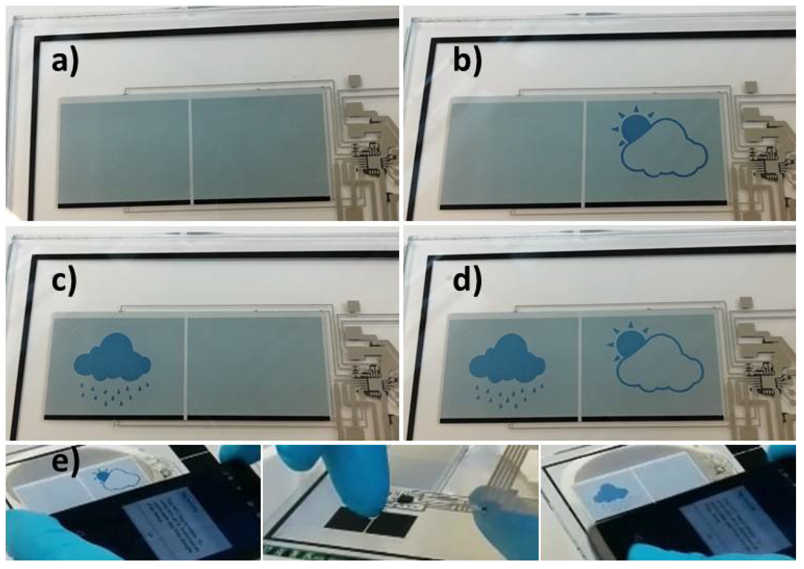
Figure 4 shows photographs of the electrochromic display upon activation of the respective segment. (a) Both segments are switched to their oxidized OFF states; (b) The sun segment is switched to its reduced ON state; (c) The sun segment is oxidized to its OFF state, and simultaneously the rain segment is switched to its reduced ON state; (d) Both segments are switched to their reduced ON states (this combination is not allowed when operating the system in sensing mode); (e) The three photographs describe one possible use case scenario. Left: The system is powered by the NFC interface of a mobile phone, a dry sensor state is monitored by the microcontroller, and the sun display segment is activated to its ON state by the microcontroller. Middle: A water droplet is added to the sensor. Right: The system is once again powered by the NFC interface of a mobile phone, a wet sensor state is monitored, and the microcontroller simultaneously switches the sun segment to its OFF state and the rain segment to its ON state. To view the full sequence, see Video S2 in the Supplementary Materials.
The energy consumption for each monitoring cycle is estimated to be less than 10 mJ for the entire system. This is based on the assumptions that the monitoring cycle time is about 5 s, the energy harvesting chip and the microcontroller together consume less than 500 µA during the monitoring cycle, 300 µC is required for the display update and a few µC are consumed during the readout of a wet sensor.

4. Conclusions

The hybrid printed electronic system presented herein demonstrates the possibility of adding different types of electronic functionalities on glass substrates. Screen printing was used to create electrochromic displays, NFC antennas, conductors, chip landing pads and sensors directly on top of transparent glass substrates, thereby also enabling see-through smart window applications. The silicon-based components were assembled using a pick-and-place process. The NFC interface allows for a batteryless sensor platform that instead relies on energy harvesting via the NFC interface of a mobile phone. A reliable 3 V signal was generated from the chip responsible for energy harvesting, which in turn served as the power supply of the sensor system. A microcontroller monitored the status of the sensor, and subsequently updated the electrochromic display to visualize the status of the sensor. Glass is a widely used material, e.g., within the automotive sector and in architectural buildings, and it can even be flexible. These features, along with its transparency and good barrier properties against moisture and oxygen penetration, makes glass a promising substrate material for future smart window applications in which many kinds of electronic functionalities can be obtained through autonomous operation.

Supplementary Materials

The following are available online at https://www.mdpi.com/article/10.3390/electronicmat2040037/s1, Video S1: Energy harvesting; Video S2: Screen printed electronic system in operation.

Author Contributions

P.A.E. and M.L. conceived the research idea. J.Å. designed the screen-printing tools and manufactured the printed electronic system using the screen-printing equipment. D.W. and A.S. finalized the system by assembling the silicon-based components using pick-and-place equipment. A.S. evaluated the adhesion of different inks screen printed onto glass substrates. P.A. selected and programmed the silicon-based components. P.A.E. performed the characterization and evaluation of the components and the final system, including data analysis. P.A.E. wrote the manuscript with contributions from all authors. All authors have read and agreed to the published version of the manuscript.

Funding

This research was funded by VINNOVA, grant number 2018-01558.

Institutional Review Board Statement

Not applicable.

Informed Consent Statement

Not applicable.

Data Availability Statement

The datasets generated during the current study are available from the corresponding author on reasonable request.

Conflicts of Interest

The authors declare no conflict of interest. The funders had no role in the design of the study; in the collection, analyses, or interpretation of data; in the writing of the manuscript, or in the decision to publish the results.

References

  1. Rim, Y.S.; Bae, S.-H.; Chen, H.; De Marco, N.; Yang, Y. Recent progress in materials and devices toward printable and flexible sensors. Adv. Mater. 2016, 28, 4415–4440. [Google Scholar] [CrossRef] [PubMed]
  2. Sekitani, T.; Someya, T. Stretchable, Large-area Organic Electronics. Adv. Mater. 2010, 22, 2228–2246. [Google Scholar] [CrossRef] [PubMed]
  3. Zheng, H.; Zheng, Y.; Liu, N.; Ai, N.; Wang, Q.; Wu, S.; Zhou, J.; Hu, D.; Yu, S.; Han, S.; et al. All-solution processed polymer light-emitting diode displays. Nat. Commun. 2013, 4, 1971. [Google Scholar] [CrossRef] [PubMed]
  4. Tobjörk, D.; Österbacka, R. Paper electronics. Adv. Mater. 2011, 23, 1935–1961. [Google Scholar] [CrossRef] [PubMed]
  5. Cao, R.; Pu, X.; Du, X.; Yang, W.; Wang, J.; Guo, H.; Zhao, S.; Yuan, Z.; Zhang, C.; Li, C.; et al. Screen-Printed Washable Electronic Textiles as Self-Powered Touch/Gesture Tribo-Sensors for Intelligent Human–Machine Interaction. ACS Nano 2018, 12, 5190–5196. [Google Scholar] [CrossRef] [PubMed]
  6. Ahmad, J.; Bazaka, K.; Anderson, L.J.; White, R.D.; Jacob, M.V. Materials and methods for encapsulation of OPV: A review. Renew. Sustain. Energy Rev. 2013, 27, 104–117. [Google Scholar] [CrossRef]
  7. Yu, D.; Yang, Y.-Q.; Chen, Z.; Tao, Y.; Liu, Y.-F. Recent progress on thin-film encapsulation technologies for organic electronic devices. Opt. Commun. 2016, 362, 43–49. [Google Scholar] [CrossRef] [Green Version]
  8. Cho, A.R.; Kim, E.H.; Park, S.Y.; Park, L.S. Flexible OLED encapsulated with gas barrier film and adhesive gasket. Synth. Met. 2014, 193, 77–80. [Google Scholar] [CrossRef]
  9. Castro-Hermosa, S.; Top, M.; Dagar, J.; Fahlteich, J.; Brown, T.M. Quantifying Performance of Permeation Barrier—Encapsulation Systems for Flexible and Glass-Based Electronics and Their Application to Perovskite Solar Cells. Adv. Electron. Mater. 2019, 5, 1800978. [Google Scholar] [CrossRef] [Green Version]
  10. Uddin, A.; Upama, M.B.; Yi, H.; Duan, L. Encapsulation of Organic and Perovskite Solar Cells: A Review. Coatings 2019, 9, 65. [Google Scholar] [CrossRef] [Green Version]
  11. Ludvigsson, M.; Leisner, P.; Schödt, B.; Dyreklev, P.; Nilssson, D.; Norberg, B.; Bäck, L.G.; Malmros, I.; Clausén, U.; Andersson Ersman, P. Laminated display based on printed electronics. In Engineered Transparency 2016—Glass in Architecture and Structural Engineering, Proceedings of Glasstec 2016, Düsseldorf, Germany, 20–23 September 2016; Schneider, J., Weller, B., Eds.; Ernst and Sohn: Berlin, Germany, 2016; ISBN 978-3-433-03187-2. [Google Scholar]
  12. Azens, A.; Granqvist, C.G. Electrochromic smart windows: Energy efficiency and device aspects. J. Solid State Electrochem. 2003, 7, 64–68. [Google Scholar] [CrossRef]
  13. Hrehorova, E.; Rebros, M.; Pekarovicova, A.; Bazuin, B.; Ranganathan, A.; Garner, S.; Merz, G.; Tosch, J.; Boudreau, R. Gravure Printing of Conductive Inks on Glass Substrates for Applications in Printed Electronics. J. Disp. Technol. 2011, 7, 318–324. [Google Scholar] [CrossRef]
  14. Epishine—Harvesting Light. Available online: https://www.epishine.com/ (accessed on 16 September 2021).
  15. Andersson Ersman, P; Lassnig, R.; Strandberg, J.; Dyreklev, P. Flexible Active Matrix Addressed Displays Manufactured by Screen Printing. Adv. Eng. Mater. 2021, 23, 2000771. [Google Scholar] [CrossRef]
  16. Andersson Ersman, P.; Lassnig, R.; Strandberg, J.; Tu, D.; Keshmiri, V.; Forchheimer, R.; Fabiano, S.; Gustafsson, G.; Berggren, M. All-printed large-scale integrated circuits based on organic electrochemical transistors. Nat. Commun. 2019, 10, 5053. [Google Scholar] [CrossRef] [Green Version]
  17. Corning Willow Glass. Available online: https://www.corning.com/worldwide/en/innovation/corning-emerging-innovations/corning-willow-glass.html (accessed on 16 September 2021).
  18. Schott—Glass Made of Ideas. Available online: https://www.schott.com/innovation/en/ultra-thin-glass-the-epic-flex/ (accessed on 16 September 2021).
  19. ASTM D3359—Standard Test Methods for Rating Adhesion by Tape Test. Available online: https://www.astm.org/Standards/D3359.htm (accessed on 4 October 2021).
  20. RISE Research Institutes of Sweden—Electrochromic Displays. Available online: https://www.ri.se/en/what-we-do/expertises/electrochromic-displays (accessed on 16 September 2021).
  21. Kawahara, J.; Andersson Ersman, P.; Engquist, I.; Berggren, M. Improving the color switch contrast in PEDOT: PSS-based electrochromic displays. Org. Electron. 2012, 13, 469–474. [Google Scholar] [CrossRef] [Green Version]
Figure 1. (a) Schematic showing a few of the screen printed layers: the first silver layer (black), the insulating layer defining the electrochromic “rain” and “sun” display segments (gray), the carbon electrodes of the sensor (orange), the insulating layer required to prevent short-circuits (green), and the second silver layer to establish wire crossings (blue); (b) The continuous voltage output level upon activating the system through the NFC interface of a mobile phone.
Electronicmat 02 00037 g001
Figure 2. Water droplets of three different volumes, thereby creating three different interface areas between the water and the carbon-based sensor electrodes, result in different current vs. time characteristics. The volumes of the three water droplets denoted small, intermediate and large correspond to approximately 100, 500 and 1000 µL, respectively.
Electronicmat 02 00037 g002
Figure 3. (a) Current vs. time switching behavior upon reduction of the respective display segment by applying 3 V to the counter electrode, i.e., coloration from white to blue. The sharp transitions at ~100–200 ms indicate that the fully reduced semiconducting state has been reached in the PEDOT:PSS electrode. Beyond this time, no further coloration occurs; (b) Current vs. time switching behavior upon oxidation of the respective display segment by applying −3 V to the counter electrode, i.e., the color is switched from blue to white.
Electronicmat 02 00037 g003
Figure 4. (ad) Photographs showing the different coloration states of the screen printed electrochromic display; (e) The photographs describe a demonstration sequence of the system, where the batteryless hybrid printed electronic sensor platform is activated by energy harvesting through the NFC interface of a mobile phone. (Left) A dry sensor state is visualized on the display. (Middle) A water drop is placed on the sensor area. (Right) A wet sensor state is visualized on the display.
Electronicmat 02 00037 g004
Publisher’s Note: MDPI stays neutral with regard to jurisdictional claims in published maps and institutional affiliations.