


Wrapping Amorphous Indium-Gallium-Zinc-Oxide Transistors with High Current Density
 , and
, and
Abstract
1. Introduction
2. Methods
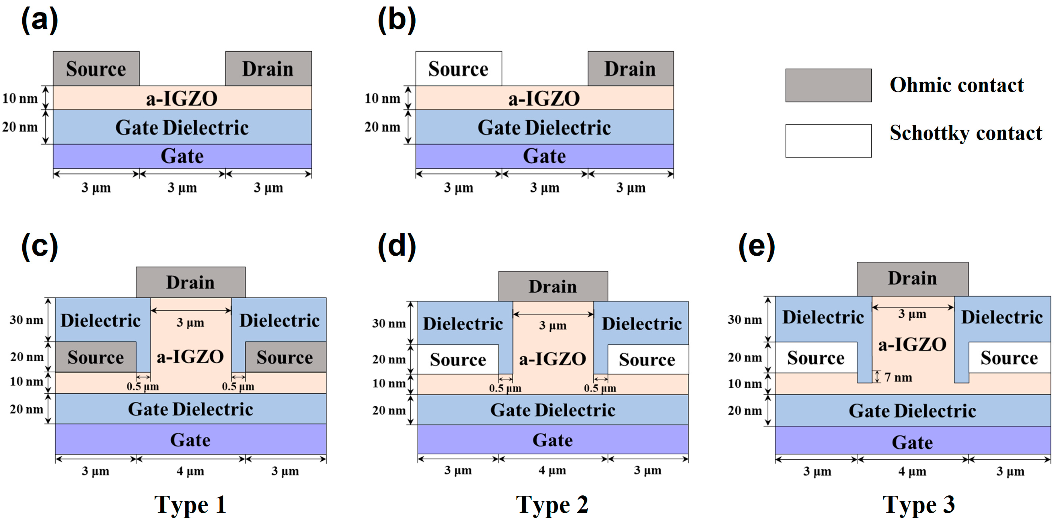
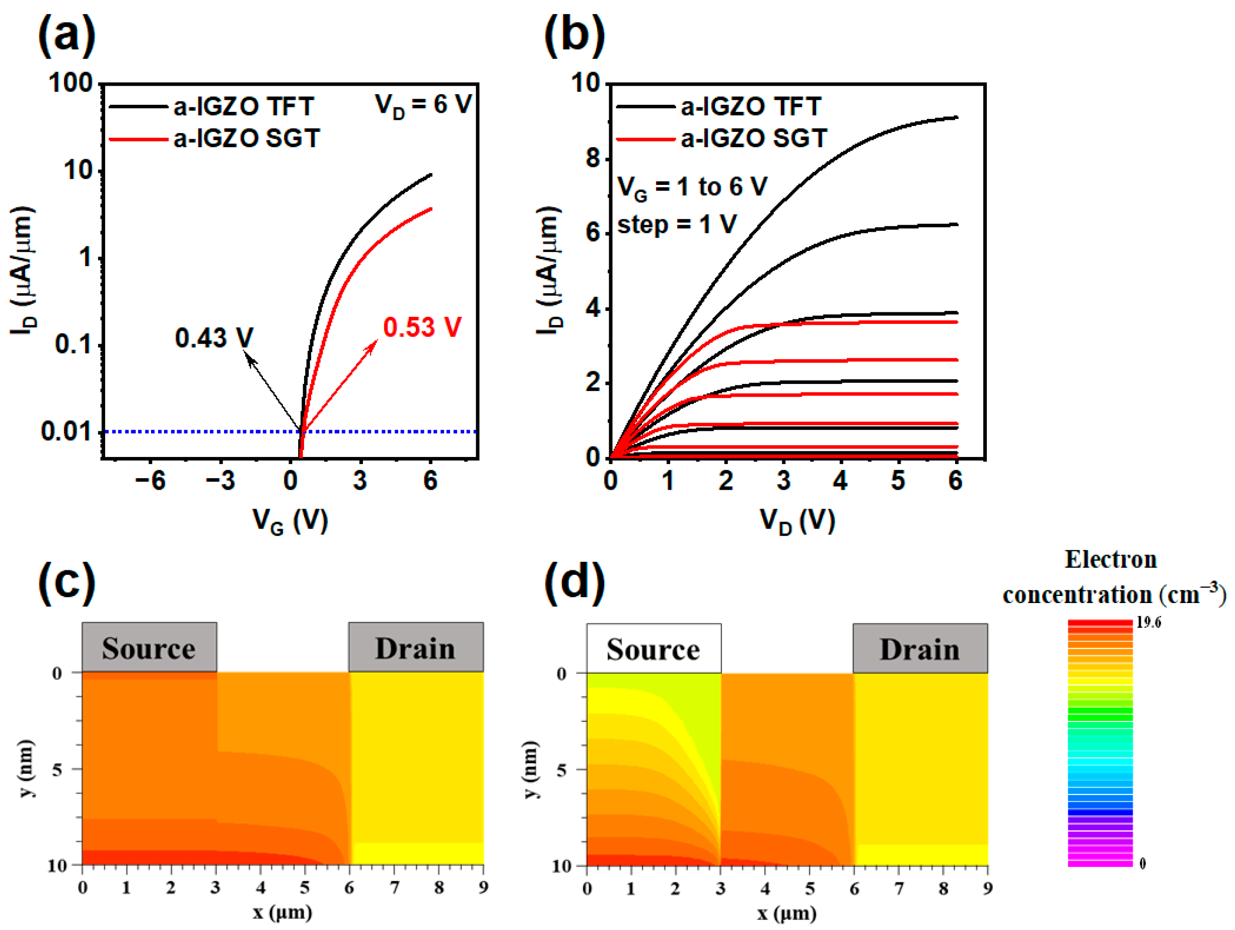
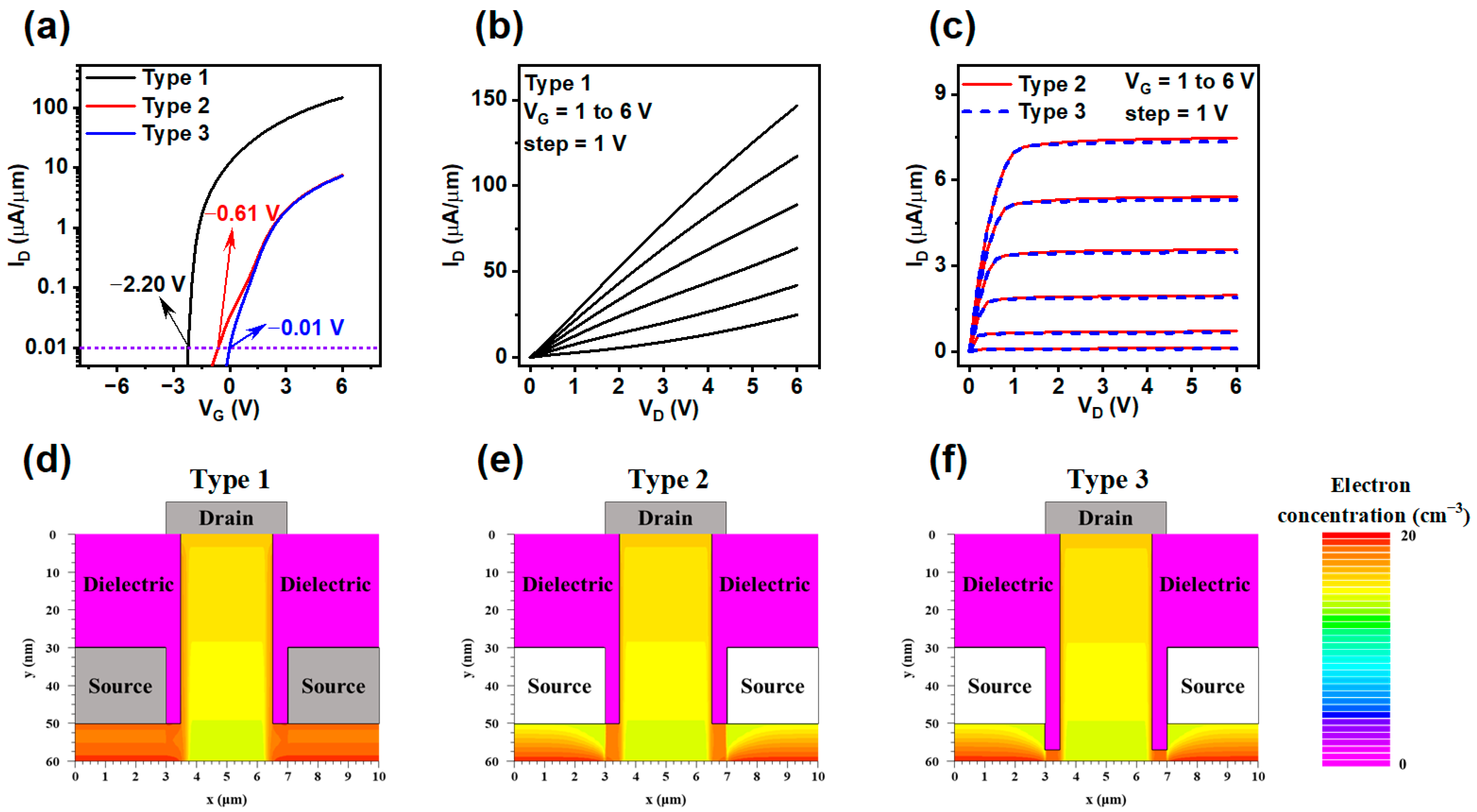
3. Results and Discussion
4. Conclusions
Author Contributions
Funding
Data Availability Statement
Conflicts of Interest
References
- Fortunato, E.; Barquinha, P.; Martins, R. Oxide Semiconductor Thin-Film Transistors: A Review of Recent Advances. Adv. Mater. 2012, 24, 2945–2986. [Google Scholar] [CrossRef]
- Ide, K.; Nomura, K.; Hosono, H.; Kamiya, T. Electronic Defects in Amorphous Oxide Semiconductors: A Review. Phys. Status Solidi A 2019, 216, 1800372. [Google Scholar] [CrossRef]
- Shim, G.W.; Hong, W.; Cha, J.-H.; Park, J.H.; Lee, K.J.; Choi, S.-Y. TFT Channel Materials for Display Applications: From Amorphous Silicon to Transition Metal Dichalcogenides. Adv. Mater. 2020, 32, 1907166. [Google Scholar] [CrossRef] [PubMed]
- Shi, J.; Zhang, J.; Yang, L.; Qu, M.; Qi, D.-C.; Zhang, K.H.L. Wide Bandgap Oxide Semiconductors: From Materials Physics to Optoelectronic Devices. Adv. Mater. 2021, 33, 2006230. [Google Scholar] [CrossRef]
- Shiah, Y.-S.; Sim, K.; Shi, Y.; Abe, K.; Ueda, S.; Sasase, M.; Kim, J.; Hosono, H. Mobility–stability trade-off in oxide thin-film transistors. Nat. Electron. 2021, 4, 800–807. [Google Scholar] [CrossRef]
- Geng, D.; Wang, K.; Li, L.; Myny, K.; Nathan, A.; Jang, J.; Kuo, Y.; Liu, M. Thin-film transistors for large-area electronics. Nat. Electron. 2023, 6, 963–972. [Google Scholar] [CrossRef]
- Park, J.S.; Maeng, W.-J.; Kim, H.-S.; Park, J.-S. Review of recent developments in amorphous oxide semiconductor thin-film transistor devices. Thin Solid Films 2012, 520, 1679–1693. [Google Scholar] [CrossRef]
- Chi, L.J.; Yu, M.J.; Chang, Y.H.; Hou, T.H. 1-V Full-Swing Depletion-Load a-In–Ga–Zn–O Inverters for Back-End-of-Line Compatible 3D Integration. IEEE Electron Device Lett. 2016, 37, 441–444. [Google Scholar] [CrossRef]
- Zhang, Y.; Li, J.; Li, J.; Huang, T.; Guan, Y.; Zhang, Y.; Yang, H.; Chan, M.; Wang, X.; Lu, L.; et al. 3-Masks-Processed Sub-100 nm Amorphous InGaZnO Thin-Film Transistors for Monolithic 3D Capacitor-Less Dynamic Random Access Memories. Adv. Electron. Mater. 2023, 9, 2300150. [Google Scholar] [CrossRef]
- Lee, S.; Chen, Y.; Jeon, J.; Park, C.; Jang, J. Reduction of Parasitic Capacitance in Indium-Gallium-Zinc Oxide (a-IGZO) Thin-Film Transistors (TFTs) without Scarifying Drain Currents by Using Stripe-Patterned Source/Drain Electrodes. Adv. Electron. Mater. 2018, 4, 1700550. [Google Scholar] [CrossRef]
- Xin, C.; Chen, L.; Li, T.; Zhang, Z.; Zhao, T.; Li, X.; Zhang, J. Highly Sensitive Flexible Pressure Sensor by the Integration of Microstructured PDMS Film With a-IGZO TFTs. IEEE Electron Device Lett. 2018, 39, 1073–1076. [Google Scholar] [CrossRef]
- Han, K.-L.; Lee, W.-B.; Kim, Y.-D.; Kim, J.-H.; Choi, B.-D.; Park, J.-S. Mechanical Durability of Flexible/Stretchable a-IGZO TFTs on PI Island for Wearable Electronic Application. ACS Appl. Electron. Mater. 2021, 3, 5037–5047. [Google Scholar] [CrossRef]
- Naqi, M.; Cho, Y.; Kim, S. High-Speed Current Switching of Inverted-Staggered Bottom-Gate a-IGZO-Based Thin-Film Transistors with Highly Stable Logic Circuit Operations. ACS Appl. Electron. Mater. 2023, 5, 3378–3383. [Google Scholar] [CrossRef]
- Son, Y.; Frost, B.; Zhao, Y.; Peterson, R.L. Monolithic integration of high-voltage thin-film electronics on low-voltage integrated circuits using a solution process. Nat. Electron. 2019, 2, 540–548. [Google Scholar] [CrossRef]
- Reinhardt, A.; von Wenckstern, H.; Grundmann, M. Metal–Semiconductor Field-Effect Transistors Based on the Amorphous Multi-Anion Compound ZnON. Adv. Electron. Mater. 2020, 6, 1901066. [Google Scholar] [CrossRef]
- Wang, G.; Zhuang, X.; Huang, W.; Yu, J.; Zhang, H.; Facchetti, A.; Marks, T.J. New Opportunities for High-Performance Source-Gated Transistors Using Unconventional Materials. Adv. Sci. 2021, 8, 2101473. [Google Scholar] [CrossRef] [PubMed]
- Zhang, J.; Wilson, J.; Auton, G.; Wang, Y.; Xu, M.; Xin, Q.; Song, A. Extremely high-gain source-gated transistors. Proc. Natl. Acad. Sci. USA 2019, 116, 4843–4848. [Google Scholar] [CrossRef] [PubMed]
- Huang, S.; Jin, J.; Kim, J.; Wu, W.; Song, A.; Zhang, J. IGZO Source-Gated Transistor for AMOLED Pixel Circuit. IEEE Trans. Electron Devices 2023, 70, 3637–3642. [Google Scholar] [CrossRef]
- Wang, Z.; Luo, L.; Wang, Y.; Zhang, J.; Song, A. Comparative Study of Short-Channel Effects Between Source-Gated Transistors and Standard Thin-Film Transistors. IEEE Trans. Electron Devices 2022, 69, 561–566. [Google Scholar] [CrossRef]
- Sihapitak, P.; Bermundo, J.P.; Bestelink, E.; Sporea, R.A.; Uraoka, Y. Optimizing a-IGZO Source-Gated Transistor Current by Structure Alteration via TCAD Simulation and Experiment. IEEE Trans. Electron Devices 2024, 71, 2431–2437. [Google Scholar] [CrossRef]
- Bestelink, E.; Niang, K.M.; Wyatt-Moon, G.; Flewitt, A.J.; Sporea, R.A. Promoting Low-Voltage Saturation in High-Performance a-InGaZnO Source-Gated Transistors. IEEE Trans. Electron Devices 2024, 71, 581–587. [Google Scholar] [CrossRef]
- Shannon, J.M.; Gerstner, E.G. Source-gated thin-film transistors. IEEE Electron Device Lett. 2003, 24, 405–407. [Google Scholar] [CrossRef]
- Shannon, J.M.; Gerstner, E.G. Source-gated transistors in hydrogenated amorphous silicon. Solid-State Electron. 2004, 48, 1155–1161. [Google Scholar] [CrossRef]
- Shannon, J.M. Stable transistors in hydrogenated amorphous silicon. Appl. Phys. Lett. 2004, 85, 326–328. [Google Scholar] [CrossRef]
- Shannon, J.M.; Dovinos, D.; Balon, F.; Glasse, C.; Brotherton, S.D. Source-gated transistors in poly-silicon. IEEE Electron Device Lett. 2005, 26, 734–736. [Google Scholar] [CrossRef]
- Sporea, R.A.; Guo, X.; Shannon, J.M.; Silva, S.R. Source-Gated Transistors for Versatile Large Area Electronic Circuit Design and Fabrication. ECS Trans. 2011, 37, 57. [Google Scholar] [CrossRef]
- Sporea, R.A.; Trainor, M.J.; Young, N.D.; Shannon, J.M.; Silva, S.R.P. Source-gated transistors for order-of-magnitude performance improvements in thin-film digital circuits. Sci. Rep. 2014, 4, 4295. [Google Scholar] [CrossRef]
- Xu, X.; Sporea, R.A.; Guo, X. Source-Gated Transistors for Power- and Area-Efficient AMOLED Pixel Circuits. J. Disp. Technol. 2014, 10, 928–933. [Google Scholar] [CrossRef]
- Baek, Y.J.; Kang, I.H.; Hwang, S.H.; Han, Y.L.; Kang, M.S.; Kang, S.J.; Kim, S.G.; Woo, J.G.; Yu, E.S.; Bae, B.S. Vertical oxide thin-film transistor with interfacial oxidation. Sci. Rep. 2022, 12, 3094. [Google Scholar] [CrossRef]
- Sun, B.; Huang, H.; Wen, P.; Xu, M.; Peng, C.; Chen, L.; Li, X.; Zhang, J. Research Progress of Vertical Channel Thin Film Transistor Device. Sensors 2023, 23, 6623. [Google Scholar] [CrossRef]
- Sheleg, G.; Greenman, M.; Lussem, B.; Tessler, N. Removing the current-limit of vertical organic field effect transistors. J. Appl. Phys. 2017, 122, 195502. [Google Scholar] [CrossRef]
- Nawaz, A.; Merces, L.; Ferro, L.M.M.; Sonar, P.; Bufon, C.C.B. Impact of Planar and Vertical Organic Field-Effect Transistors on Flexible Electronics. Adv. Mater. 2023, 35, 2204804. [Google Scholar] [CrossRef] [PubMed]
- Martins, J.; Kiazadeh, A.; Pinto, J.V.; Rovisco, A.; Gonçalves, T.; Deuermeier, J.; Alves, E.; Martins, R.; Fortunato, E.; Barquinha, P. Ta2O5/SiO2 Multicomponent Dielectrics for Amorphous Oxide TFTs. Electron. Mater. 2021, 2, 1–16. [Google Scholar] [CrossRef]
- Robertson, J. High dielectric constant oxides. Eur. Phys. J. Appl. Phys. 2004, 28, 265–291. [Google Scholar] [CrossRef]
- Zhao, D.; Li, J.; Kakkad, R.; Du, Z.; Hu, S.; Chen, J.; Hu, S.; Liu, G. 1: Challenges of TFT Technology for AMOLED Display. SID Symp. Dig. Tech. Pap. 2019, 50, 1–8. [Google Scholar] [CrossRef]


| Parameters | IGZO |
|---|---|
| Carrier concentration | 1 × 1016 cm−3 |
| Mobility | 10 cm2/Vs |
| Electron affinity | 4.16 eV |
| Band gap | 3.05 eV |
Disclaimer/Publisher’s Note: The statements, opinions and data contained in all publications are solely those of the individual author(s) and contributor(s) and not of MDPI and/or the editor(s). MDPI and/or the editor(s) disclaim responsibility for any injury to people or property resulting from any ideas, methods, instructions or products referred to in the content. |
© 2025 by the authors. Licensee MDPI, Basel, Switzerland. This article is an open access article distributed under the terms and conditions of the Creative Commons Attribution (CC BY) license (https://creativecommons.org/licenses/by/4.0/).
Share and Cite
Liu, J.; Huang, S.; Xiao, Z.; Li, N.; Kim, J.; Jin, J.; Zhang, J. Wrapping Amorphous Indium-Gallium-Zinc-Oxide Transistors with High Current Density. Electron. Mater. 2025, 6, 2. https://doi.org/10.3390/electronicmat6010002
Liu J, Huang S, Xiao Z, Li N, Kim J, Jin J, Zhang J. Wrapping Amorphous Indium-Gallium-Zinc-Oxide Transistors with High Current Density. Electronic Materials. 2025; 6(1):2. https://doi.org/10.3390/electronicmat6010002
Chicago/Turabian StyleLiu, Jiaxin, Shan Huang, Zhenyuan Xiao, Ning Li, Jaekyun Kim, Jidong Jin, and Jiawei Zhang. 2025. "Wrapping Amorphous Indium-Gallium-Zinc-Oxide Transistors with High Current Density" Electronic Materials 6, no. 1: 2. https://doi.org/10.3390/electronicmat6010002
APA StyleLiu, J., Huang, S., Xiao, Z., Li, N., Kim, J., Jin, J., & Zhang, J. (2025). Wrapping Amorphous Indium-Gallium-Zinc-Oxide Transistors with High Current Density. Electronic Materials, 6(1), 2. https://doi.org/10.3390/electronicmat6010002