
Transmitters and Receivers for High Capacity Indoor Optical Wireless Communication


Abstract
1. Introduction
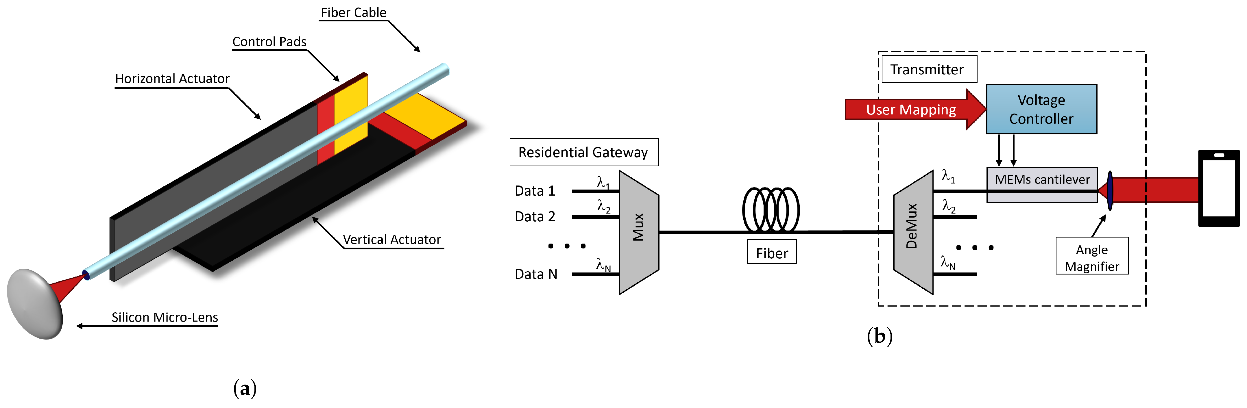
2. Beam-Steering for Optical Wireless Communications Transmitter
2.1. Introduction
2.2. State of the Art for Narrow Beam-Steering
2.3. Transmitter Experimental Setup
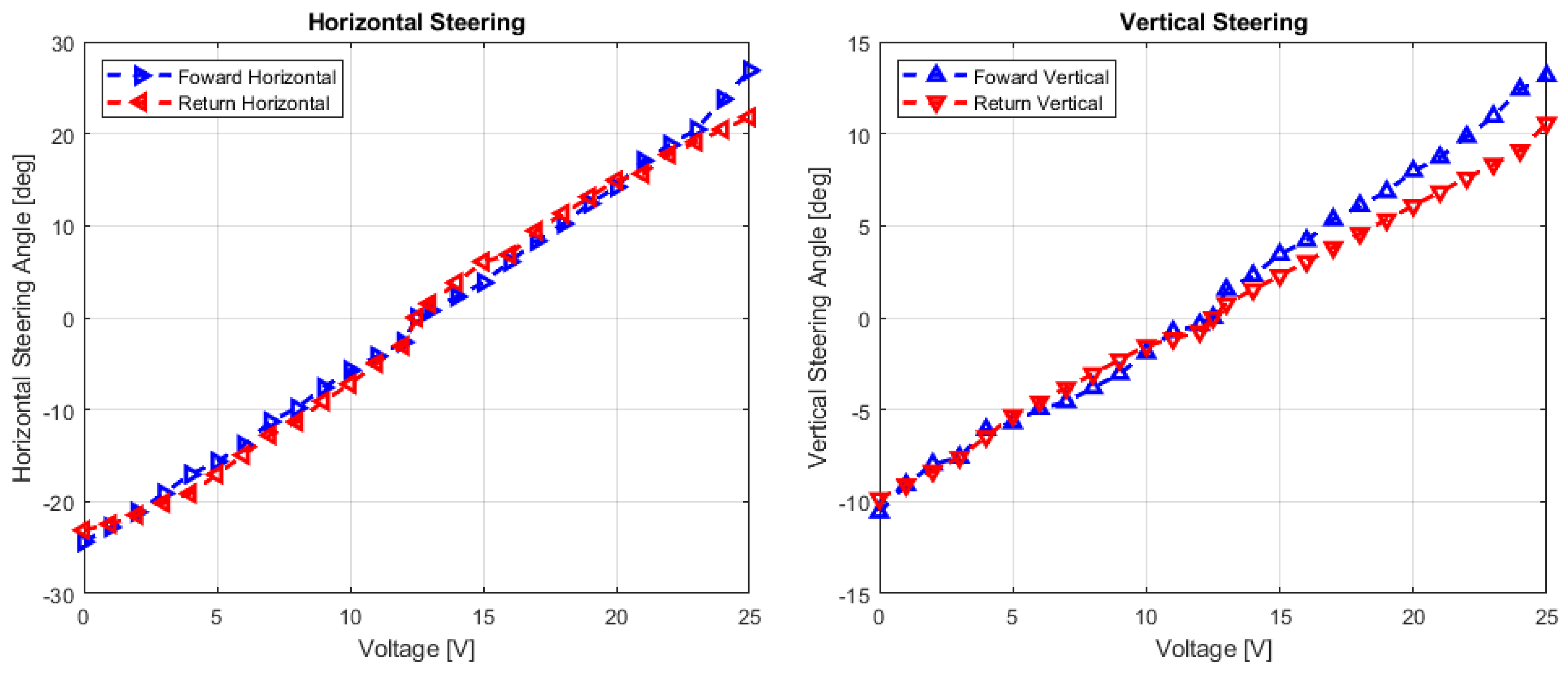
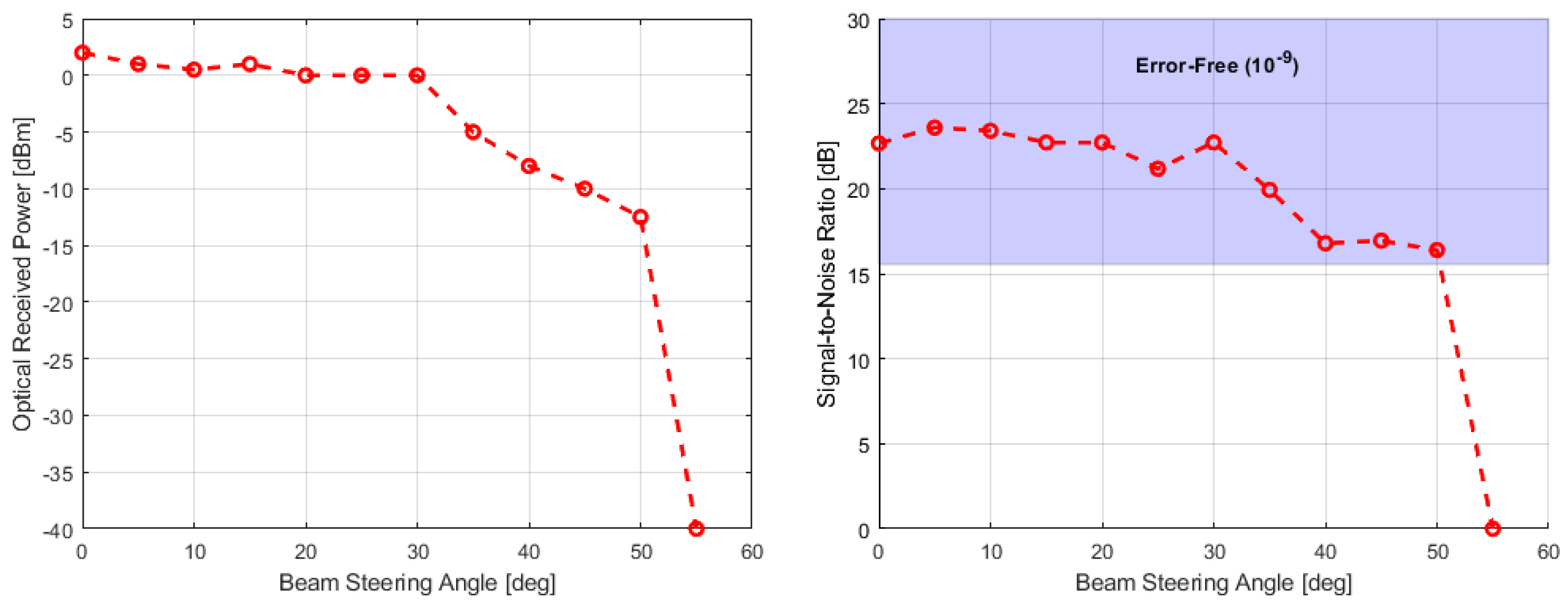
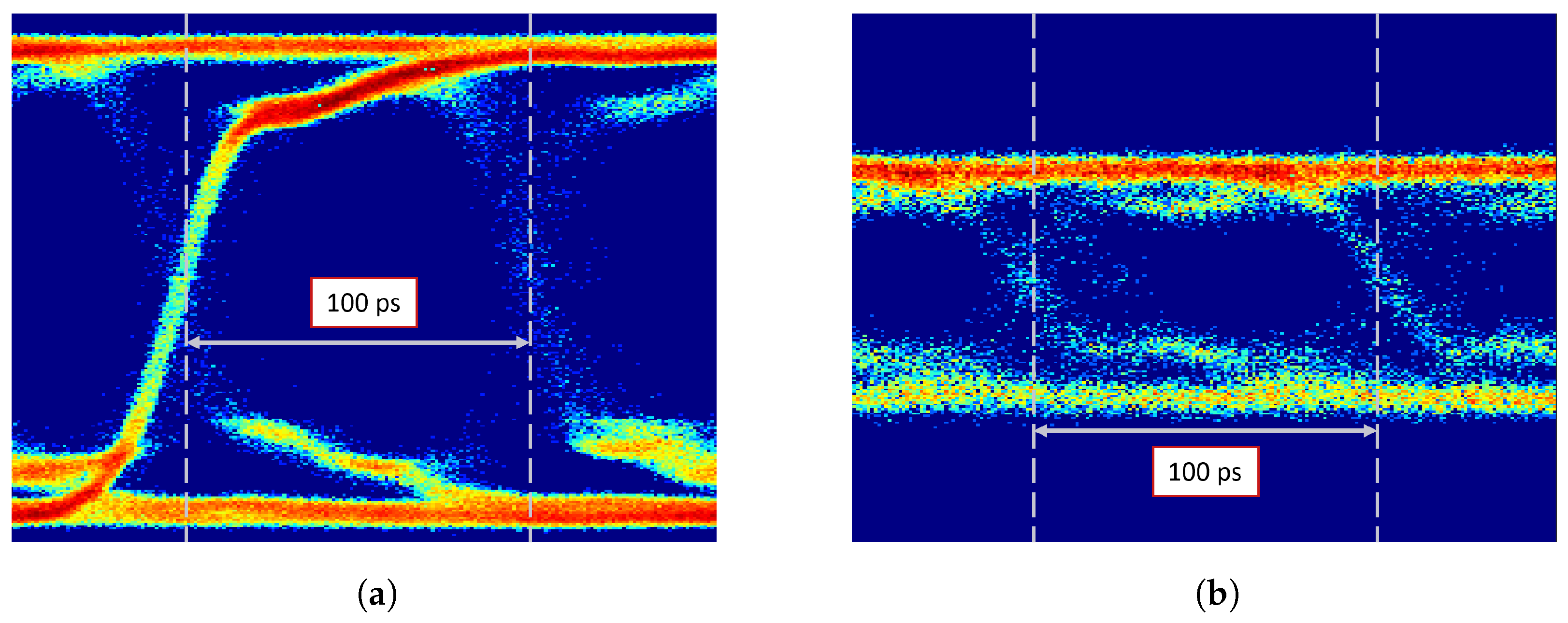
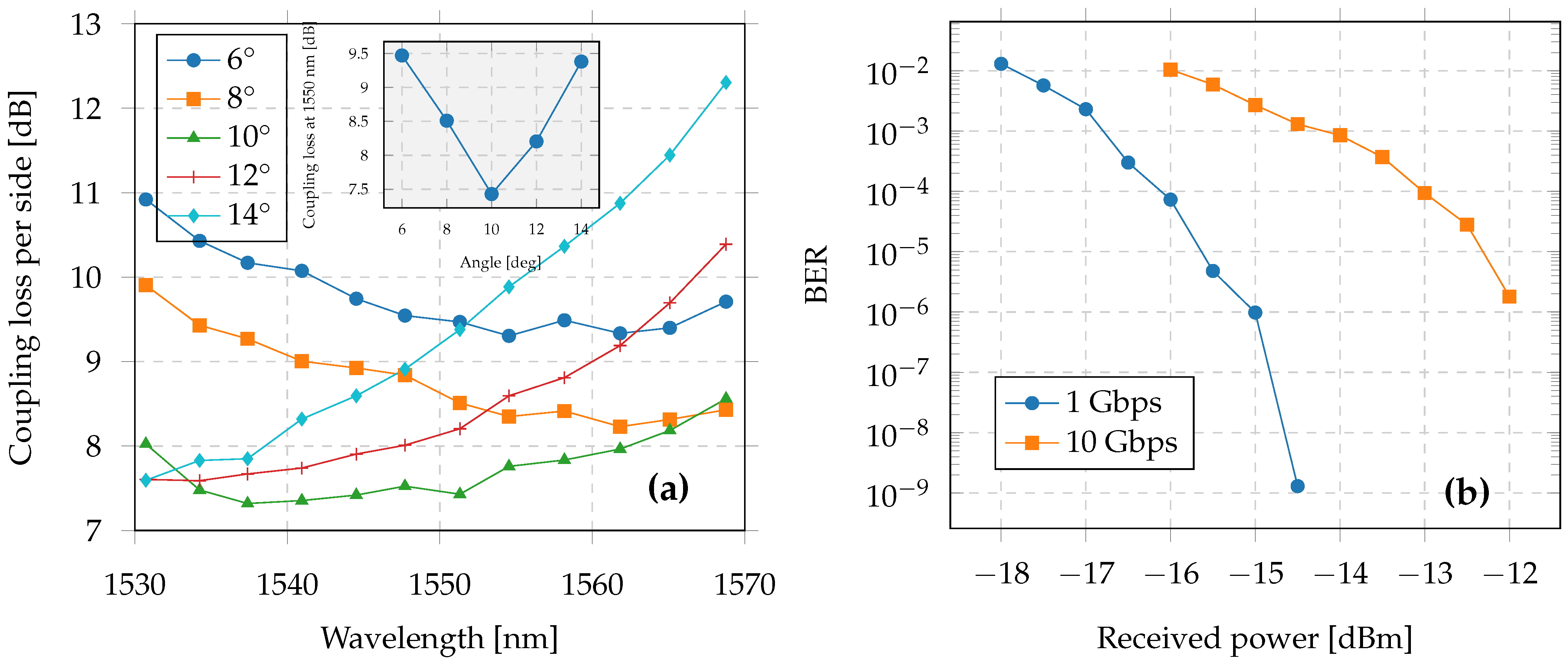
2.4. Experimental Results
3. Receiver for Optical Wireless Communication
3.1. Introduction
3.2. State-of-the-Art
Indium-Phosphide Membrane on Silicon
3.3. Quad Photodiode Array
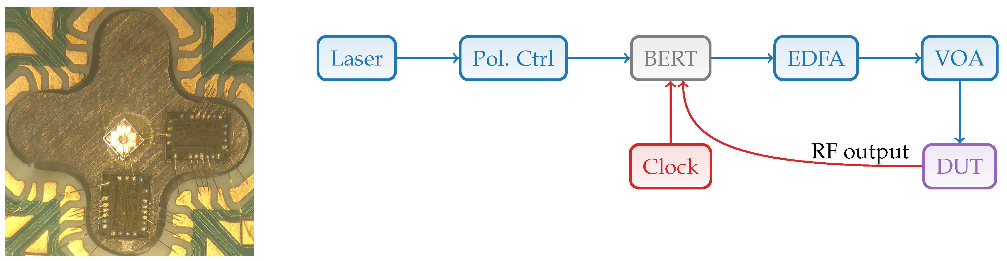
3.3.1. Description
3.3.2. Experiment
3.3.3. Results
3.4. WDM OWC Receiver with a Single Surface Grating Coupler
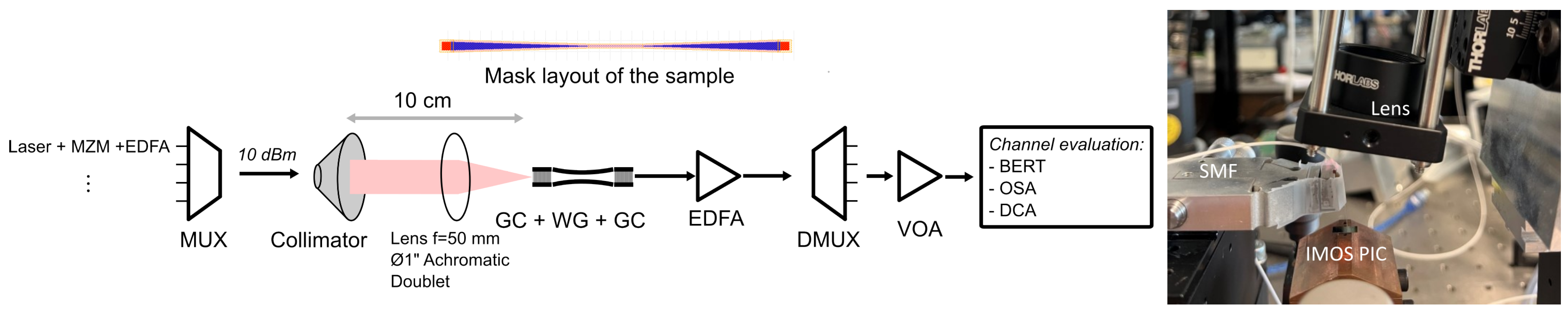
3.4.1. Introduction
3.4.2. Experiment
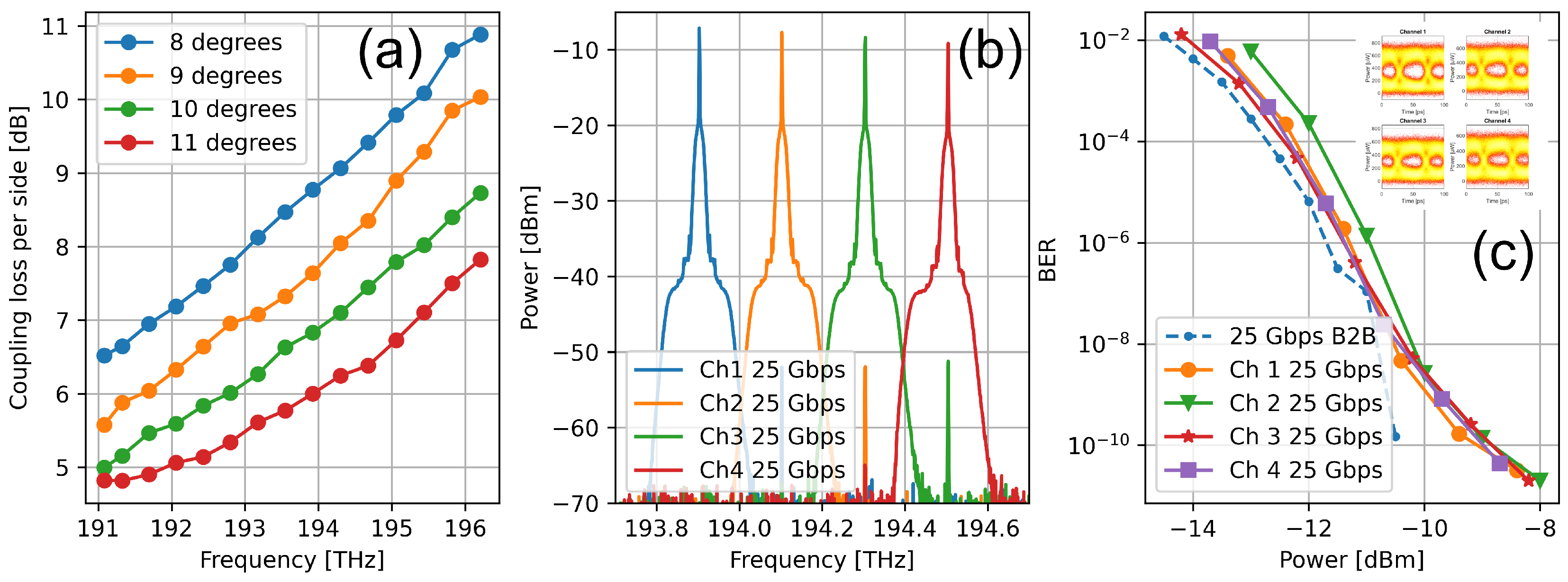
3.4.3. Results
3.5. OWC Receiver with an Array of Surface Grating Couplers
3.5.1. Description
3.5.2. Experiment
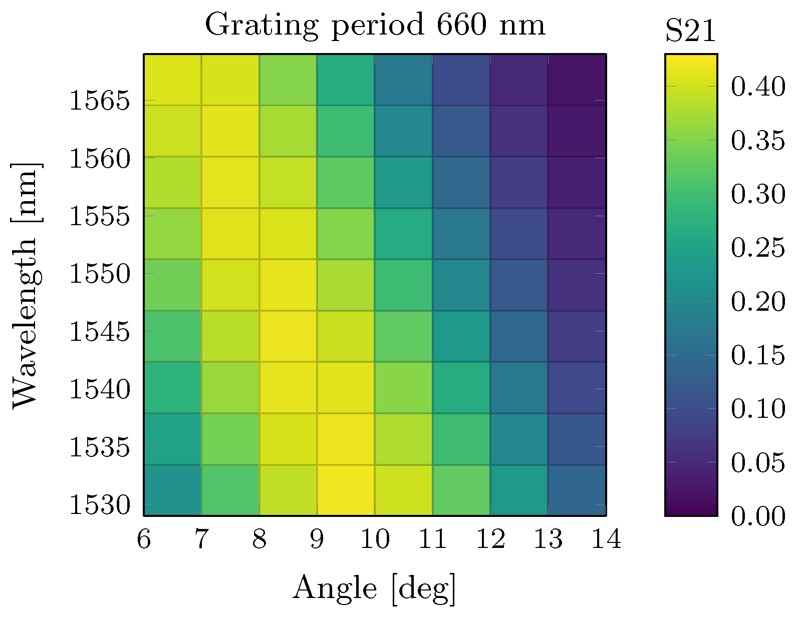
3.5.3. Results
4. Conclusions
Author Contributions
Funding
Institutional Review Board Statement
Informed Consent Statement
Data Availability Statement
Acknowledgments
Conflicts of Interest
Abbreviations
| ADR | Angle Diversity Receiver |
| AR | Anti-Reflection |
| AWGN | Additive White Gaussian Noise |
| AWGR | Arrayed Waveguide Grating Router |
| BER | Bit Error Rate |
| BERT | Bit Error Rate Tester |
| DCA | Digital Communication Analyzer |
| DUT | Device Under Test |
| EDFA | Erbium Doped Fiber Amplifier |
| FEC | Forward Error Correction |
| FoV | Field of View |
| IMOS | Indium-Phosphide Membrane on Silicon |
| IR | Infrared Light |
| ITU | International Telecommunication Union |
| MEMs | Micro Electrical-Mechanical systems |
| MMI | Multi-Mode Interferometer |
| MMF | Multi-Mode Fiber |
| MZM | Mach-Zehnder Modulator |
| NRZ | Non-return-to-zero |
| OOK | On Off Keying |
| OSA | Optical Spectrum Analyzer |
| OSNR | Optical Signal to Noise Ration |
| OWC | Optical Wireless Communication |
| PIC | Photonic Integrated Circuit |
| PRBS | Pseudo-Random Binary Sequence |
| PZT | Piezo-Electric Transducers |
| SDM | Space Division Multiplexing |
| SLM | Spatial Light Modulators |
| SNR | Signal to Noise Ratio |
| TIA | Trans-Impedance Amplifier |
| VCSEL | Vertical-cavity surface-emitting laser |
| VOA | Variable Optical Attenuator |
| WDM | Wavelength Division Multiplexing |
References
- Wei, Z.; Wang, Z.; Zhang, J.; Li, Q.; Zhang, J.; Fu, H. Evolution of optical wireless communication for B5G/6G. Prog. Quantum Electron. 2022, 83, 100398. [Google Scholar] [CrossRef]
- Koonen, T.; Mekonnen, K.; Cao, Z.; Huijskens, F.; Pham, N.Q.; Tangdiongga, E. Ultra-high-capacity wireless communication by means of steered narrow optical beams. Philos. Trans. R. Soc. 2020, 378, 20190192. [Google Scholar] [CrossRef] [PubMed]
- Koonen, T. Indoor optical wireless systems: Technology, trends, and applications. J. Light. Technol. 2018, 36, 1459–1467. [Google Scholar] [CrossRef]
- Hoy, C.; Stockley, J.; Shane, J.; Kluttz, K.; McKnight, D.; Serati, S. Non-Mechanical Beam Steering with Polarization Gratings: A Review. Crystals 2021, 11, 361. [Google Scholar] [CrossRef]
- Yu, D.; Lou, S.; Ou, X.; Yu, P.; Duan, H.; Hu, Y. Polarization Independent Dynamic Beam Steering based on Liquid Crystal Integrated Metasurface. Sci. Rep. 2024, 14, 23627. [Google Scholar] [CrossRef] [PubMed]
- Doylend, J.K.; Heck, M.J.R.; Bovington, J.T.; Peters, J.D.; Coldren, L.A.; Bowers, J.E. Two-dimensional free-space beam steering with an optical phased array on silicon-on-insulator. Opt. Express 2011, 19, 21595. [Google Scholar] [CrossRef]
- Gomez, A.; Quintana, C.; Faulkner, G.; O’Brien, D. Point-to-Multipoint Holographic Beamsteering Techniques for Indoor Optical Wireless Communications; SPIE: San Francisco, CA, USA, 2016; p. 97720Q. [Google Scholar] [CrossRef]
- Cardarelli, S.; Calabretta, N.; Stabile, R.; Williams, K.; Luo, X.; Mink, J. Wide-Range 2D InP Chip-to-Fiber Alignment Through Bimorph Piezoelectric Actuators. In Proceedings of the 2018 IEEE 68th Electronic Components and Technology Conference (ECTC), San Diego, CA, USA, 29 May–1 June 2018; IEEE: Piscataway, NJ, USA, 2018; pp. 1124–1129. [Google Scholar] [CrossRef]
- Muller, E.; Song, Y.; Koonen, T.; Tangdiongga, E. Beam-Forming and -Steering in Optical Wireless Communication using Piezoelectric Actuators and Micro-Lenses. In Proceedings of the 50th European Conference on Optical Communications (ECOC 2024), Frankfurt, Germany, 22–26 September 2024; pp. 1267–1270. [Google Scholar]
- Elsheikh, O.E.; Swillam, M.A. Wide-angle non-uniform optical phased array using compact and efficient antenna design. Sci. Rep. 2024, 14, 3780. [Google Scholar] [CrossRef]
- Pedrotti, F.L.; Pedrotti, L.M.; Pedrotti, L.S. Matrix Methods in Paraxial Optics, 3rd ed.; Cambridge University Press: Cambridge, UK, 2017; pp. 396–418. [Google Scholar] [CrossRef]
- Franta, D.; Dubroka, A.; Wang, C.; Giglia, A.; Vohánka, J.; Franta, P.; Ohlídal, I. Temperature-dependent dispersion model of float zone crystalline silicon. Appl. Surf. Sci. 2017, 421, 405–419. [Google Scholar] [CrossRef]
- Barua, B. Comparison the Performance of Free-Space Optical Communication with OOK and BPSK Modulation under Atmospheric Turbulence. Int. J. Eng. Sci. Technol. 2011, 3, 4391–4399. [Google Scholar]
- Mekonnen, K.; Gelinck, G. Modified Angle Diversity Receiver with Wide Field-of-View for Short-Range High-Speed Optical Wireless Communication. In Proceedings of the 50th European Conference on Optical Communications (ECOC 2024), Frankfurt, Germany, 22–26 September 2024; Volume 2024, pp. 1–4. [Google Scholar]
- Umezawa, T.; Matsumoto, A.; Akahane, K.; Nakajima, S.; Yamamoto, N. Large Submillimeter High-Speed Photodetector for Large Aperture FSO Receiver. IEEE J. Sel. Top. Quantum Electron. 2022, 28, 1–9. [Google Scholar] [CrossRef]
- Hirakawa, K.; Harada, S.; Ohnuki, Y.; Umezawa, T.; Matsumoto, A.; Akahane, K.; Yamamoto, N.; Kawanishi, T. Monolithic Integrated 2D Micro-Lens Array Design with High-Speed 2D-Photodetector Array. In Proceedings of the 2024 IEEE Photonics Conference (IPC), Rome, Italy, 10–14 November 2024; pp. 1–2. [Google Scholar] [CrossRef]
- Weng, Z.K.; Yoshida, Y.; Umezawa, T.; Bekkali, A.; Hattori, M.; Matsumoto, A.; Kanno, A.; Yamamoto, N.; Kawanishi, T.; Akahane, K. 40-Gbit/s Mobile FSO with High-speed Beam Stabilizer and 2D-PDA-based Diversity Receiver for Support Robots. In Proceedings of the 2024 Optical Fiber Communications Conference and Exhibition (OFC), Los Angeles, CA, USA, 15–19 March 2024; pp. 1–3. [Google Scholar]
- Wolny, M.; Henader, S.; Mink, J.; Koonen, A.; Tangdiongga, E. Quad photodiode array for optical wireless communication. In Proceedings of the IEEE Benelux Chapter Annual Symposium 2022, IEEE Photonics Benelux Chapter Annual Symposium 2022, Virtual, 24–25 November 2022. [Google Scholar]
- Sarbazi, E.; Kazemi, H.; Crisp, M.; El-Gorashi, T.; Elmirghani, J.; Penty, R.V.; White, I.H.; Safari, M.; Haas, H. Design and Optimization of High-Speed Receivers for 6G Optical Wireless Networks. IEEE Trans. Commun. 2024, 72, 971–990. [Google Scholar] [CrossRef]
- Song, Y.M.; Xie, Y.; Malyarchuk, V.; Xiao, J.; Jung, I.; Choi, K.J.; Liu, Z.; Park, H.; Lu, C.; Kim, R.H.; et al. Digital cameras with designs inspired by the arthropod eye. Nature 2013, 497, 95–99. [Google Scholar] [CrossRef] [PubMed]
- Brandl, P.; Enne, R.; Jukić, T.; Zimmermann, H. OWC Using a Fully Integrated Optical Receiver With Large-Diameter APD. IEEE Photonics Technol. Lett. 2015, 27, 482–485. [Google Scholar] [CrossRef]
- Kakarla, R.; Schröder, J.; Andrekson, P.A. One photon-per-bit receiver using near-noiseless phase-sensitive amplification. Light. Sci. Appl. 2020, 9, 153. [Google Scholar] [CrossRef] [PubMed]
- Peyronel, T.; Quirk, K.J.; Wang, S.C.; Tiecke, T.G. Luminescent detector for free-space optical communication. Optica 2016, 3, 787–792. [Google Scholar] [CrossRef]
- Riaz, A.; Collins, S. A wide field of view VLC receiver for smartphones. In Proceedings of the 2020 European Conference on Optical Communications (ECOC), Brussels, Belgium, 6–10 December 2020; pp. 1–4. [Google Scholar] [CrossRef]
- Traverso, A.J.; Huang, J.; Peyronel, T.; Yang, G.; Tiecke, T.G.; Mikkelsen, M.H. Low-loss, centimeter-scale plasmonic metasurface for ultrafast optoelectronics. Optica 2021, 8, 202–207. [Google Scholar] [CrossRef]
- Wang, S.; Le-Van, Q.; Peyronel, T.; Ramezani, M.; Van Hoof, N.; Tiecke, T.G.; Gómez Rivas, J. Plasmonic Nanoantenna Arrays as Efficient Etendue Reducers for Optical Detection. ACS Photonics 2018, 5, 2478–2485. [Google Scholar] [CrossRef]
- Shalaginov, M.Y.; An, S.; Yang, F.; Su, P.; Lyzwa, D.; Agarwal, A.M.; Zhang, H.; Hu, J.; Gu, T. Single-Element Diffraction-Limited Fisheye Metalens. Nano Lett. 2020, 20, 7429–7437. [Google Scholar] [CrossRef]
- García-Márquez, J.; Valencia-Estrada, J.C. Freeform concentrator design for IR wireless-to-fiber link communications. J. Opt. Soc. Am. A 2023, 40, 1741–1752. [Google Scholar] [CrossRef]
- Winston, R.; Jiang, L.; Ricketts, M. Nonimaging optics: A tutorial. Adv. Opt. Photon. 2018, 10, 484–511. [Google Scholar] [CrossRef]
- Graaf, J.; Zhao, X.; Konstantinou, D.; van den Hout, M.; Reniers, S.; Shen, L.; van der Heide, S.; Rommel, S.; Tafur Monroy, I.; Okonkwo, C.; et al. Beyond 110 GHz uni-traveling carrier photodiodes on an InP-membrane-on-silicon platform. IEEE J. Sel. Top. Quantum Electron. 2022, 28, 1–10. [Google Scholar] [CrossRef]
- Milanizadeh, M.; SeyedinNavadeh, S.; Zanetto, F.; Grimaldi, V.; De Vita, C.; Klitis, C.; Sorel, M.; Ferrari, G.; Miller, D.A.B.; Melloni, A.; et al. Separating arbitrary free-space beams with an integrated photonic processor. Light. Sci. Appl. 2022, 11, 197. [Google Scholar] [CrossRef] [PubMed]
- Xu, L.; Chen, X.; Li, C.; Tsang, H.K. Bi-wavelength two dimensional chirped grating couplers for low cost WDM PON transceivers. Opt. Commun. 2011, 284, 2242–2244. [Google Scholar] [CrossRef]
- Cheng, L.; Mao, S.; Zhao, C.; Tu, X.; Li, Q.; Fu, H.Y. Three-Port Dual-Wavelength-Band Grating Coupler for WDM-PON Applications. IEEE Photonics Technol. Lett. 2021, 33, 159–162. [Google Scholar] [CrossRef]
- Wolny, M.; Deng, W.; Reniers, S.; Koonen, A.; Tangdiongga, E. 100 Gbps WDM OWC Link Performance Using IMOS Surface Grating Coupler and Commercial Fiber Receivers. In Proceedings of the Optical Fiber Communication Conference (OFC), San Diego, CA, USA, 24–28 March 2024; Optica Publishing Group: Washington, DC, USA, 2024. [Google Scholar] [CrossRef]
- Wolny, M.; Sosa, M.P.; de Graaf, J.; Koonen, A.; Tangdiongga, E. Surface Grating Coupler Array for Optical Wireless Communication Receivers. In Proceedings of the 2024 International Topical Meeting on Microwave Photonics—MWP, Pisa, Italy, 17–20 September 2024; Institute of Electrical and Electronics Engineers: Piscataway, NJ, USA, 2024. [Google Scholar]
- van der Tol, J.J.G.M.; Jiao, Y.; Shen, L.; Millan-Mejia, A.; Pogoretskii, V.; van Engelen, J.P.; Smit, M.K. Indium Phosphide Integrated Photonics in Membranes. IEEE J. Sel. Top. Quantum Electron. 2018, 24, 1–9. [Google Scholar] [CrossRef]


| Metric | This Paper | Metasurfaces [5] | OPA [10] | SLM [7] | AWGR [2] |
|---|---|---|---|---|---|
| Field of View | 51.3° × 22.4° | 54.2° | 160° | 60° | 17° × 17° |
| Throughput | 10 Gbps | NA | NA | 224 Gbps | 112 Gbps |
| Steering Type | Continuous | Discrete | Discrete | Discrete | Discrete |
| Multi-Beams | No | No | No | Yes | Yes |
| Wavelength | 1550 nm | 950 nm | 1550 nm | 1550 nm–1600 nm | 1550 nm |
Disclaimer/Publisher’s Note: The statements, opinions and data contained in all publications are solely those of the individual author(s) and contributor(s) and not of MDPI and/or the editor(s). MDPI and/or the editor(s) disclaim responsibility for any injury to people or property resulting from any ideas, methods, instructions or products referred to in the content. |
© 2025 by the authors. Licensee MDPI, Basel, Switzerland. This article is an open access article distributed under the terms and conditions of the Creative Commons Attribution (CC BY) license (https://creativecommons.org/licenses/by/4.0/).
Share and Cite
Wolny, M.; Muller, E.; Tangdiongga, E. Transmitters and Receivers for High Capacity Indoor Optical Wireless Communication. Telecom 2025, 6, 26. https://doi.org/10.3390/telecom6020026
Wolny M, Muller E, Tangdiongga E. Transmitters and Receivers for High Capacity Indoor Optical Wireless Communication. Telecom. 2025; 6(2):26. https://doi.org/10.3390/telecom6020026
Chicago/Turabian StyleWolny, Mikolaj, Eduardo Muller, and Eduward Tangdiongga. 2025. "Transmitters and Receivers for High Capacity Indoor Optical Wireless Communication" Telecom 6, no. 2: 26. https://doi.org/10.3390/telecom6020026
APA StyleWolny, M., Muller, E., & Tangdiongga, E. (2025). Transmitters and Receivers for High Capacity Indoor Optical Wireless Communication. Telecom, 6(2), 26. https://doi.org/10.3390/telecom6020026