1. Introduction
Energy Harvesting (EH) is a method within the realm of renewable energy exploitation that primarily involves capturing minute amounts of ambient energy, stemming from either natural sources or human actions, which would normally go untapped. EH is typically deployed in remote or challenging environments where access to the electrical grid is unavailable, yet there is a requirement to power essential electronic circuits. The Internet of Things (IoT) domain serves as a prime illustration of this concept [
1,
2].
Kinetic Energy Harvesters (KEHs) among the array of designed devices stand out as they transform vibrations into electrical energy via the utilization of electromagnetic generators or smart materials like piezoelectrics and magnetostrictives. KEHs employing magnetostrictive materials primarily harness the Villari effect (or inverse magnetostrictive effect) and Faraday’s law. This method holds significant promise in providing power to low-power electronic systems, such as Wireless Sensor Networks (WSNs). These networks find applications, for instance, in the Structural Health Monitoring (SHM) of bridges and viaducts [
3,
4]. More details on working principles exploited by KEH can be found in [
5,
6,
7,
8].
Magnetostrictive materials like
Galfenol exhibit favorable mechanical properties, possess high energy density, and display minimal sensitivity to temperature variations. Importantly, while piezoelectric materials suffer from issues such as cracking and depolarization, magnetostrictive materials are metals alloys [
9,
10]. Conversely, the latter ones are susceptible to robust non-linear and hysteresis effects. Consequently, the amount of harvested energy relies on magnetic bias and mechanical pre-stress, needing appropriate modeling techniques [
11,
12].
Figure 1 illustrates the design of a
force-driven energy harvester using Galfenol as its core material. This device leverages the inverse magnetostrictive (
Villari) effect to respond to the varying force applied at the top, resulting in fluctuations in magnetic flux density within the active material. Subsequently, the harvester generates an electrical voltage across a coil wrapped around the magnetostrictive material, operating in accordance with Faraday’s law [
13]. In addition, a secondary coil can be employed to monitor the output characteristics and initiate a Power Electronic Interface (PEI) circuit. This PEI circuit serves the purpose of optimizing the connection between the KEH and the intended load. A comprehensive analysis of the entire potential harvester has been conducted using fully integrated non-linear Finite Element Method (FEM) modeling [
14], and preliminary experimental tests [
15] have been previously reported in related research works.
On the contrary, in
velocity-driven harvesters, the mechanical stress is not directly applied to the active material. Instead, the approach involves harnessing the surrounding environmental vibrations to induce acceleration. In such cases, a common design for the harvester is a cantilever beam. The choice between using one type of harvester over the other depends on the characteristics of the environmental vibrations. Force-driven harvesters are typically employed when there is a high level of mechanical stress and a broad range of vibration frequencies. In contrast, velocity-driven harvesters are preferred when vibrations exhibit a narrower frequency range, and the cantilever is designed to operate under resonance conditions. Moreover, the power density extracted from these harvesters varies, with force-driven harvesters yielding power densities in the range of about 10–30 mW/cm
, while velocity-driven harvesters can achieve higher power densities ranging from 20 to 200 mW/cm
[
8].
Magnetostrictive KEHs frequently encounter irregular input forces due to the unpredictable nature of their energy sources. In such circumstances, employing an appropriate PEI, as AC–DC boost converters, can yield significant advantages. Depending on the specific operating conditions, this power conditioning system serves the dual purpose of optimizing the efficiency of the energy harvesting system [
17] and of increasing the available voltage output. It is worth noting that the conventional AC-to-DC conversion stage typically comprises a passive diode bridge followed by a DC–DC Buck or Boost converter. However, the use of a passive full bridge rectifier inherently leads to power losses and a decrease in overall power efficiency [
18,
19,
20,
21]. To achieve higher conversion efficiency, an alternative solution involves employing an AC–DC converter (active full bridge), which is still an extensively researched approach in the present day [
18,
19,
21,
22,
23]. Aside from efficiency enhancements, such an implementation could lead to a more streamlined and lighter KEH. Indeed, as mentioned earlier, the harvester already incorporates an inductor, which not only offers economic benefits but also holds the promise of simultaneously reducing losses and minimizing the device’s dimensions [
24].
Preliminary experiments were performed and compared with the simulations’ results in [
16]. Here, the experimental setup has been enriched and output performances, in different operating working conditions and output parameters, have been studied. The paper is organized as described below. In
Section 2, the AC–DC boost switching converter is introduced and its operation is analyzed, while the experimental setup is described. In
Section 3, the new experimental results are reported and discussed. The Conclusions section ends the paper.
2. Experimental Setup
AC–DC boost converters operate based on the precise timing of transistor “ON-OFF” switching, positioned within a dedicated circuit to enable voltage regulation at the output. In this context, it is possible to elevate the DC voltage to a specific level without the necessity of transformers or amplifiers. During the “ON” phase (when the switches are closed), magnetic energy is stored within an inductor. Subsequently, during the “OFF” phase (when the switches are opened one at a time), this stored energy is released in a controlled manner into the output stage, often comprising an RC filter. By fine tuning the circuit parameters, including the Duty Cycle (
D) and Time Delay (
), remarkably high levels of conversion efficiency can be attained, typically falling within the range of 80–
[
17,
25,
26,
27]. Due to the irregular and non-periodic nature of the input for KEH, it becomes essential to employ a controller capable of
real-time measurement of input fluctuations and of triggering the circuit accordingly. In our research, we advocate the use of a low-cost controller, such as Arduino, and proceed to experimentally validate its effectiveness in controlling the AC–DC boost process. Arduino boards are ideal for trial studies since they are highly configurable and programmable for different purposes.
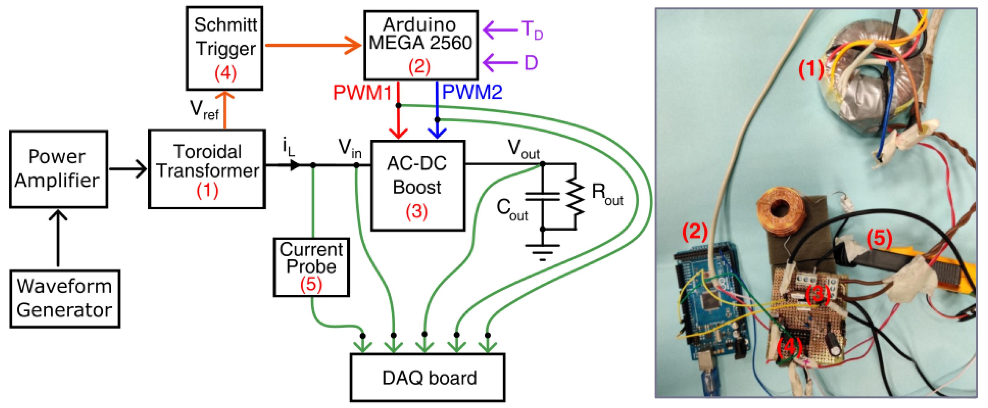
Figure 2 illustrates the electrical configuration of the full-wave AC–DC boost Converter which serves as the focus of our study. In this setup,
represents the generic AC source, while
L and
represent the inductance and internal resistance of the inductor, respectively. As illustrated in the figure, two MOSFETs function as controlled switches. The gates of the MOSFETs are connected to two distinct Pulse Width Modulation (PWM) signals that are generated by the Arduino board. These PWM signals, influenced by parameters
and
D, enable the regulation of the output voltage (
) across the load resistor (
) [
16,
24].
Detailed information regarding the circuit parameters and the model of electronic components used in this study can be found in
Table 1.
Here, the experimental setup has been designed to serve as a proof of concept for demonstrating the AC–DC boosting effect on an unidentified AC source.
Figure 3 shows the setup scheme where the AC–DC boost circuit, described in the previous section, is fed by one of the secondary windings of a 150 VA transformer with an RMS value of about 155 mV. The inset of
Figure 3 shows a picture of the actual experimental setup, where the main devices and components used are identifiable. The transformer output current corresponds to the inductor one (
) and is measured using a non-contact current clamp (model: Fluke i30s). The latter has a working frequency range up to 100 kHz, which is far above the signal frequencies used in the experimental measurements (<100 Hz). The primary winding of the transformer is fed by a power amplifier (model: KEPCO BOP 50-20MG), driven by an arbitrary waveform voltage generator (model: Aim-TTi TGA12104). The boost charges an RC (resistive–capacitive) load, where the resistive load is fixed at 2.2 k
, while the capacitor has been changed in order to study its output performances (10, 100, and 330 μF). The gates of the MOSFETs are driven by two digital outputs of an Arduino Mega 2560 board. It is worth noting that those PWMs signals are a further input of power to the system. But, the latter can be neglected because of the very low input currents of MOSFETs’ gates (in the order of hundreds of nA) and has not been considered in all the figures of merit in the following. A Schmitt trigger is devoted to intercept the sign changes in the input AC signal, via a secondary winding referenced to ground. Indeed, because of the floating nature of the AC–DC boost input, a second winding has been exploited to have a phase signal for triggering. This is not an issue for magnetostrictive KEHs, as explained in the introduction. Furthermore, a data acquisition board (model: National Instruments SCXI-1000 + NI 1520 board), at a 30 kS/s sampling frequency, measures and acquires the input voltage (
), the inductor current (
), the two Arduino PWMs, and the voltage over the capacitor–resistor parallel (
). The input voltage is measured in differential mode, while all the other voltages are measured in single-ended mode. It is worth noting that the choice of the 2.2 k
output resistor is the result of a tradeoff between the need to represent the load of a generic low-power wireless sensor node and to obtain a reasonable ripple of the output voltage with the adopted capacitors.
The Arduino board is the control unit. The Schmitt trigger drives a digital input, exploited as an interrupt pin. This interrupt is considered as the reference timing. The difference between two interrupt events is the AC signal period. Then, the two controllable parameters D and , expressed in percents of the time period T, are real-time translated into effective timing for the PWM signals. This piece of code is very important because it allows, in perspective, to deal with non-periodic, non-deterministic input signals, as expected for a true energy-harvesting application.
3. Measurements and Discussion
This work can be considered an evolution of the conference work presented in [
16]. Indeed, by driving the transformer primary with a waveform signal generator, it is possible to evaluate the proposed PEI behavior at different input frequency conditions. Other performance parameters such as efficiency and ripple factor, under different operating conditions, were also evaluated in this work.
Table 2 shows the main differences between the two works. It is noticeable that here the considered input voltage
is very low, thus emulating the
dim output of an energy harvester.
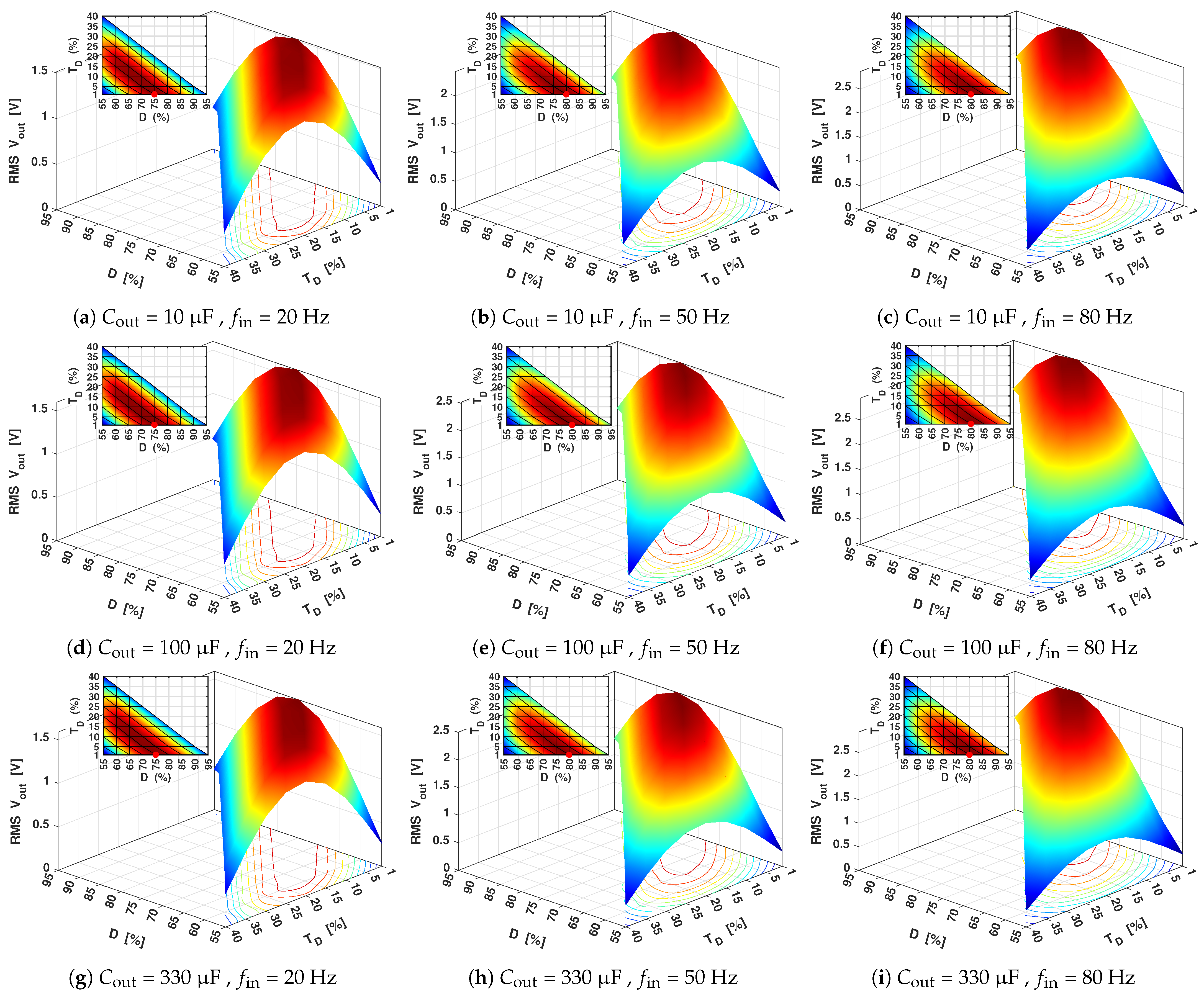
Many experimental measurements have been performed using the setup described in the previous section. In particular, different sinusoidal signals have been generated by the arbitrary waveform generator to drive the power amplifier and then applied to the toroidal transformer. Furthermore, input voltages at a constant amplitude with three different frequencies (i.e., 20, 50, and 80 Hz) and three different output capacitors (i.e., 10, 100, and 330
F) have been exploited. Furthermore, the controllable parameters
D and
have been varied and the output voltage measured. The circuit of
Figure 2 has been implemented, and the experimental
and PWMs signals have been used as inputs of the circuit.
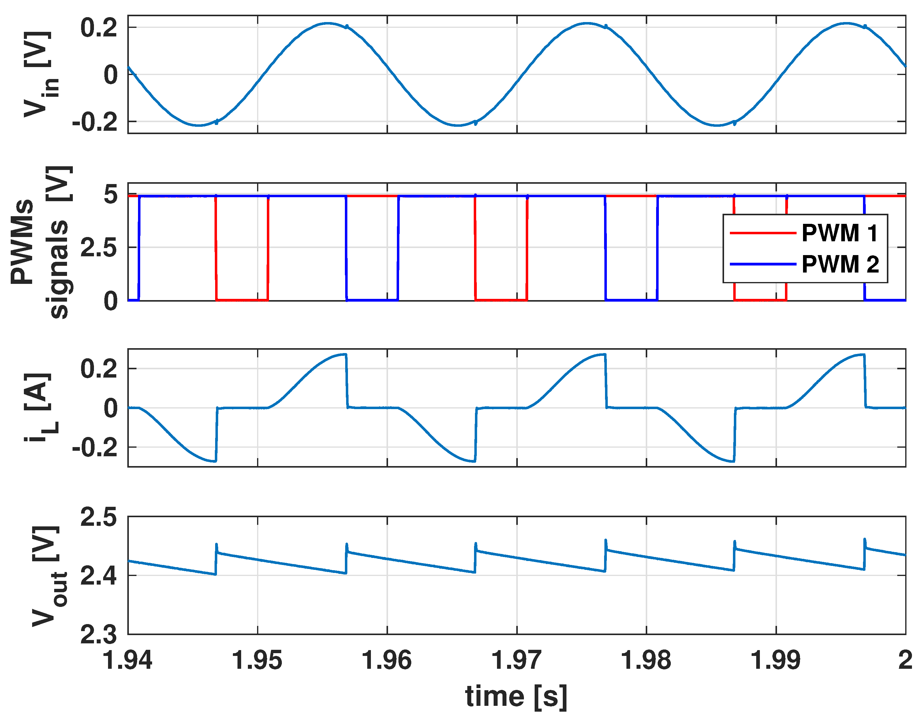
Figure 4 shows the input voltage, PWMs signals, inductor current, and output voltage in steady state, with
= 330
F, while
= 1% and
D = 80%, which are the optimal controllable parameters at
= 50 Hz, as will be shown in the following. The PWM1 signal rises when the input voltage changes signs by positively crossing zero and falls after about 15 ms, i.e.,
T, while the PWM2 signal is
forward shifted with respect to PWM1, as expected. Finally, the current profile shows that the energy stored in the inductor discharges on the capacitor–resistor parallel load after each intersection between the two “ON” states of the PWM signals, then when both MOSFETs are closed.
It is worth to note that, in order to boost the output DC voltage, the following conditions should be addressed:
, i.e., the inductor should be short-circuited on the AC input, and then charge in a certain time interval;
, i.e., the delay and “ON” timing of the two PWM signals should belong to a time period T of the AC input ( of the time period T).
As a consequence, the following plots of the RMS output voltage, efficiency, and ripple factor are triangular matrices with respect to and D.
In
Figure 5, it is reported a mapping of the RMS output voltage surfaces with respect to different values of Time Delay, Duty Cycle, input voltage frequency, and output capacitor. The surfaces have similar shapes and show peaks in the working conditions where the circuit behaves as a boost, while the shapes rapidly decreases near the above-mentioned boundary conditions. As expected, by increasing the input frequency, the RMS output voltage maxima also increases because of the related switching frequency which depends on
. Thus, the peaks’ RMS output voltage increases from 1.52 V (at
= 20 Hz) up to 2.86 V (at
= 80 Hz) for
= 10
F. Conversely, the peaks’ RMS output voltage slightly changes with respect to the output capacitor. However, for
= 100
F, it shows the maximum values of 1.60, 2.52, and 2.94 V at 20, 50, and 80 Hz, respectively, which correspond to a voltage gain factor of about 10, 16, and 19 V/V. The corresponding peaks of the RMS powers are about 1.2, 3, and 4 mW, respectively.
About the controllable parameters, the
–
D pair that maximizes the output voltage are placed on an almost straight zone, as shown by the insets of
Figure 5a–i, then by confirming the results achieved by the authors with preliminarily circuit simulations in [
24]. In particular, maximum RMS output voltages are achieved at
= 1% and
D = 75% for
= 20 Hz, while at
= 1% and
D = 80% for
, they are equal to 50 and 80 Hz, respectively.
An important performance factor to take into account, when exploiting an electronic interface for harvesting purposes, is the conversion efficiency. The AC–DC boost efficiency
, expressed in %, is computed as:
where
is the RMS input power, computed in a steady-state condition as:
with
, i.e., the instantaneous input power, while
is the RMS output power, computed as:
It is important to underline that the power absorbed by the AC–DC system via the PWMs signals is neglected in the computation of input power of Equation (
2), as motivated above. It is known that the discrepancy between input and output powers is represented by the power losses (
), which is manly due to the switching, conduction, and passive devices losses [
28].
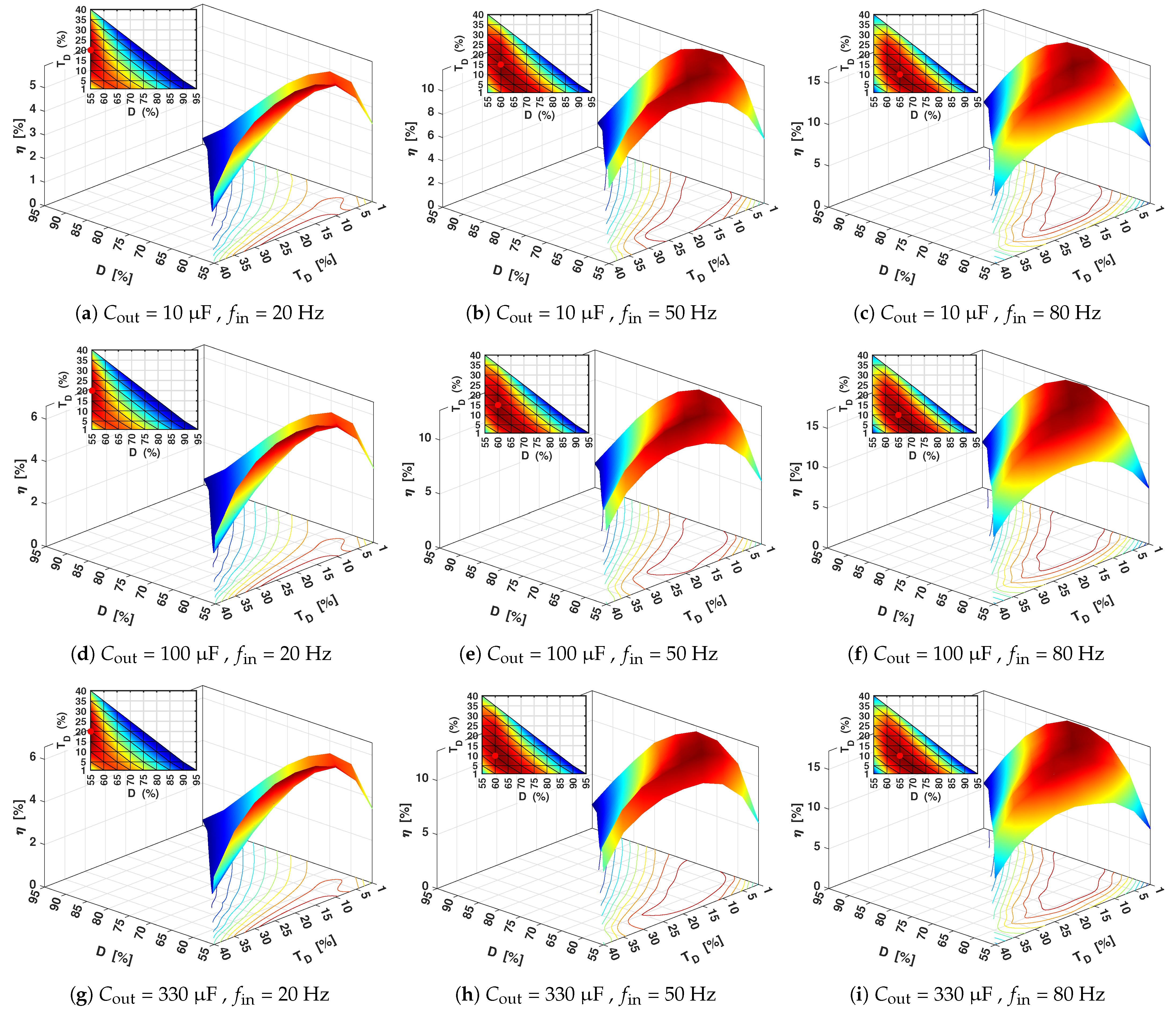
Figure 6 shows a mapping of the power efficiencies of the considered AC–DC boost, with respect to the Time Delay and Duty Cycle, input voltage frequency, and output capacitor. As expected, it is noticeable that the efficiency increases with respect to the increasing input frequency
because of the correlated increasing in switching frequency. Moreover, it is observable that the efficiency peaks are located in low
D and intermediate
values regions at 20 Hz (
is about 6%), while they shift towards slightly higher
D and lower
within increasing the input frequency (
is about 17% at 80 Hz). Furthermore, the peaks’ efficiency are very weakly affected by the output capacity
.
In particular, the peaks’ efficiency variations, with respect to the output capacity, is limited to below 1% for all the considered input frequency values.
It is worth pointing out that, even if the achieved peaks’ efficiency, which are included in a range from about 6% to 17%, could appear as very low values, they are much greater than KEH energy conversion efficiencies shown in the literature, which range in units or tenths of % [
29]. Furthermore, the power efficiency of a KEH could not be merely defined as the ratio of electrical output power and mechanical input power. Indeed, when considering EH world, this definition fails to consider various crucial factors, such as the significant influence of device design on the input mechanical power. Consequently, it is often preferable to lean towards employing certain figures of merit (FoM), as the ones reported in [
30].
An important design factor to be considered in designing an AC–DC converter is the Ripple Factor (
). Indeed, in order to reduce the size of converters, it would be necessary to use small inductors and capacitors, with a corresponding increasing in
value, which is strongly undesirable. Indeed, the higher the
value, the higher the non-ideality into the DC output voltage waveform, due to the rectification process. An estimation of the signal shape is the Form Factor (
), which is defined as [
31]:
where
and
are the RMS and average output voltage computed in steady state, respectively. A measure of the ripple content of a signal is then the Ripple Factor, defined as [
31]:
In
Figure 7, it shows a mapping of Ripple Factors in the considered AC–DC boost, with respect to the Time Delay and Duty Cycle, input voltage frequency, and output capacitor. It can be noticed that the ripple is very hardly affected by controllable parameters
and
D; indeed, each surface appears substantially flat. Conversely,
is directly affected by the input voltage frequency
, and thus, by the switching frequency. Indeed, by quadrupling
, the
is scaled by a factor of about 4, for each
. As expected, the output capacity strongly concerns the
value: the greater the capacity, the greater is the discharging time on the output resistor. In particular, the results shown in
Figure 7a–i suggest that a 10
F capacitance should be avoided for the AC–DC boost used in these working conditions, while for the 100 and 330
F output capacitance, the designed boost converter seems to have a low harmonic content in the output voltage, which is a desirable property.


 ,
, 


