Article

Combined Light and Data Driving Stages without Capacitors for Energy Transformation

1
Faculty Electronic Engineering & Entrepreneurship, University of Applied Sciences Technikum Wien, 1200 Vienna, Austria
2
Automation, Computers, Electrical and Energy Engineering Department, University of Petrosani, 332006 Petrosani, Romania
*
Author to whom correspondence should be addressed.
Electricity 2024, 5(2), 313-333; https://doi.org/10.3390/electricity5020016
Submission received: 17 April 2024 / Revised: 13 May 2024 / Accepted: 13 May 2024 / Published: 5 June 2024
(This article belongs to the Special Issue Electricity in 2024)

Abstract

:
Three LED drivers which can be used for illumination, but whose main task is the transmission of information (data) via the light of the LEDs, are explored in this paper. The converter circuits need no capacitors for the energy transformation and avoid an inrush current. The lack of necessity of electrolytic capacitors reduces cost and space. Dimming the illumination is also easy to achieve. The control concept of the converters and the generation of pulsing of the LEDs for transmitting the information (data) are explained. The converters can also be expanded to more stages to drive more LEDs with different types of information. All three converters are explained in detail; all presented circuits are built up and simulated with LTSpice. Several data transmission concepts are applied and demonstrated through simulations.

1. Introduction

Supplying light emitting diodes (LEDs) with converters which have no electrolytic capacitors reduces the cost and improves the reliability of the system. Three converter topologies which do not need large capacitors are explored in this paper. Furthermore, these converters can be used for illumination, but they are also able to transmit data via light. The use of LEDs for illumination and for data transmission is a topic which has a bright future. Ref. [1] proposes a general concept for vehicle-to-vehicle (V2V) communication by using visible light. Ref. [2] shows the use of visible light communication in indoor environments, as each light unit is multiplexed with a unique tone for transmission. Using dimming, light with pulse width modulation (PWM) and quadrature amplitude modulation (QAM) is discussed in [3]. LED arrays based on GaN are proposed in [4] for illumination and high-speed visible light communication. Combined illumination dimming on PWM and visible light communication based on a discrete multitone signal can be found in [5]. The optimization of the illumination performance of trichromatic white LEDs and the characterization of the modulation bandwidth for communication applications are addressed in [6]. Ref. [7] shows a study of illumination and communication using organic LEDs. So far, in [1,2,3,4,5,6,7], different concepts of light data transmission and LED technologies are mentioned. Ref. [8] shows several modulation concepts and a high dynamic current source for LED light and data transmission applications. The application of visible light communication for industrial IoT and the necessary interference management based on reconfigurable photodetectors are discussed in [9]. A combination of data and optical power transmission across a single fiber for high-voltage applications is shown in [10], where a classical Boost converter with a large output capacitor is used. Interesting LED drivers for optical wireless communication (but also needing large capacitors) are presented in [11]. Experiments on vehicle-to-vehicle (V2V) communication via light can be found in [12]. In [13], indoor experimental validation and performance analysis for simultaneous illumination and communication using commercial white LED lamps are explored. Ref. [14] discusses a vehicle-based internet system based on the automotive headlight. The application of visible light commutation is useful in airplanes, buildings, at home, and in cars, with multiple input and multiple output quadrature modulation being explained in [15]. A constant current control circuit for a primary-side controlled AC-DC LED driver based on the flyback converter (with an output capacitor) is explained in [16]. Up to this point, in [10,11], and [16], different converters with output capacitors are discussed, and in some of them, inrush currents can also occur. Ref. [17] shows a resonant switched-capacitor auxiliary circuit for active power decoupling in electrolytic capacitor-less AC/DC LED drivers. Ref. [18] explores a multi-channel low-power LED driver for medical application. A highly efficient LED driver based on a hybrid DC-DC converter can be found in [19]. An LED driver with a power factor corrector (PFC) without electrolytic capacitors (but still relatively large capacitors) is shown in [20]. In [17,18,19,20], different LED driver circuits with various control concepts and applications are described. In this context, no data transmission via light communication is applied.

2. Driving Stage I

Figure 1 shows the basic circuit. The converter is based on the Buck converter and consists of the main electronic switch SM, the inductor L1, and the diode DM. The capacitor at the outside is replaced by LEDs. The diode D1 must only be used when the LED load is not able to switch off quickly. Power LEDs have larger reverse recovery currents when switched off quickly. This occurs when using LEDs for illumination. The current through the load is equal to the current through the coil. With the switch SP, the current through the load can be pulsed. An advantage of this LED driver circuit is that no capacitor is necessary for the energy transformation. This leads to a cheaper and more reliable design.
The best way to operate this converter is by a bang–bang current controller. With this controller, the current can be held within a band; the smaller the hysteresis of the controller, the smaller the tolerance band of the current, but the higher the switching frequency. When the converter is not pulsed, two modes exist. In the first mode M1, the electronic switch SM is on, DM is off, and the current flows from the input source through the switch SM, the inductor, and the load. In mode M2, the transistor is turned off and the current through the inductor free-wheels through the diode DM and the load. The voltage across the LEDs can be described by a crack characteristic with a fixed voltage VLED and a differential resistor RLED. In this model, the crack voltage VD and the differential resistor RD of the load diode D1 are included. The change in the current through the inductor during M1 is described by the differential equation
d i L d t = u 1 ( V L E D + R L E D · i L ) L .
The current increases. When the electronic switch SM is turned off, the free-wheeling diode DM turns on and the current decreases according to
d i L d t = ( V L E D + R L E D · i L ) L .
With a hysteresis controller, a near-constant current through the coil IL0 is produced. When the transistor is on, the current increases by ΔI:
U 1 ( V L E D + R L E D · I L 0 ) = L Δ I T o n .
One can calculate the necessary on-time of the active switch according to
d i L d t = ( V L E D + R L E D · i L ) L .
When the active switch turns off, the current decreases by ΔI within the off-time Toff:
( V L E D + R L E D · I L 0 ) = L Δ I T o f f .
The off-time can now be given by
T o f f = L Δ I V L E D + R L E D · I L 0 .
One can now calculate the period of the controller, when only the modes M1 and M2 are used (no pulsing with SP occurs):
T M 1 M 2 = T o n + T o f f = L Δ I U 1 U 1 ( V L E D + R L E D · I L 0 ) ( V L E D + R L E D · I L 0 ) .
The switching frequency of the hysteresis controller is therefore
f M 1 M 2 = 1 T o n + T o f f = U 1 ( V L E D + R L E D · I L 0 ) ( V L E D + R L E D · I L 0 ) L Δ I U 1 .
Changes in the input voltage or changes in the parameters of the load change only the frequency of the controller and therefore of the converter. So, the control is very robust. The accuracy of the current is given by the hysteresis. A smaller hysteresis and/or a smaller inductor lead to a higher switching frequency.
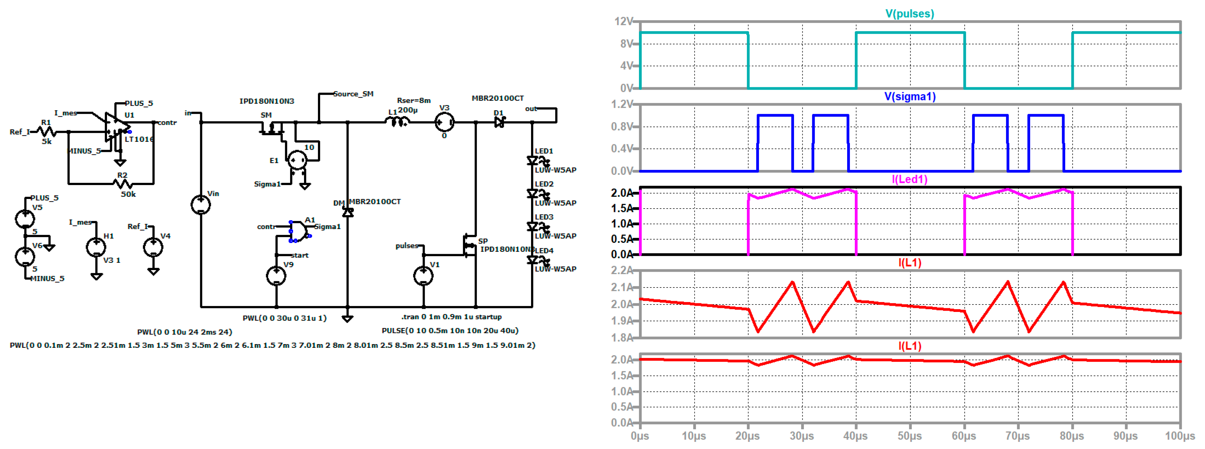
When the light has to be pulsed to dim the illumination or to produce significant changes in the radiation, such as when the system is used for, e.g., disinfection purposes or to send information, a third mode has to occur. In mode M3, the switch SP is on and the inductor is nearly short-circuited. Using a MOSFET with only a few mΩ as the resistor and a Schottky diode for the free-wheeling diode DM, the current through the inductor stays nearly constant. Figure 2 shows the control signals of the main and the pulse switch, as well as the currents through the coil and the load. The current through the coil changes around 2 A, the frequency without pulsing is about 175 kHz and the hysteresis is about 300 mA. The input voltage is 48 V. The simulation circuit is also shown in Figure 2. The controller is realized by the comparator U1. The hysteresis of the controller is fixed by the resistors R1 and R2. The current through the coil is measured and transferred by the current-controlled voltage source H1. This signal is compared with the voltage of the arbitrary voltage source V4 which produces the reference value. The high-side driver, which is necessary for the high-side switch, is built by the voltage-controlled voltage source E1. The control signal Sigma1, which is the output signal of the and gate A1, is amplified by the factor 10.
With an input voltage of 24 V, one obtains longer on-times of the main switch SM. The switching frequency is lower (compared to Figure 2), which can be seen in Figure 3, but the current is still around the desired value (Figure 3, bottom traces).
A reduction in the input voltage leads to a longer on-time of the main switch SM. The pulsed load is still supplied by a near-constant current (Figure 4).
The here-described driving circuit is very easy to realize and a relatively high data rate can be achieved.

2.1. Pulsing of More Channels in Series

To achieve more channels in the series, MOSFETs could be connected to groups of LEDs (Figure 5). To each LED or group of LEDs which can be short-circuited by an electronic switch SP, a diode is connected in the series to avoid a large reverse recovery time of the LEDs. The simulation circuit is shown in Figure 5. Three pulse switches SP are used. Now, two additional high-side drivers are used. It should be mentioned that other switches like p-channel MOSFET can simplify the control of the switches SP.
Figure 6 shows the current through the three LEDs, the control signal of the main switch SM, the control signals for pulsing the three LEDs, and the current ripple of the current through the coil.
With three LEDs and using different types of LEDs (red, green, and blue), one can now code the information into three channels and the information can be included in the pulse length and in the phase shifts between the pulses. Furthermore, one can change the chrominance and the color temperature.

2.2. Variation in the Arrangement of the Inductor L1, the Main Switch SM, and the Diode DM

In Figure 7a, the negative terminal of the input is connected with the negative side of the load. The variant according to Figure 7b has the advantage that the main switch is connected to ground; the output side, however, is floating.
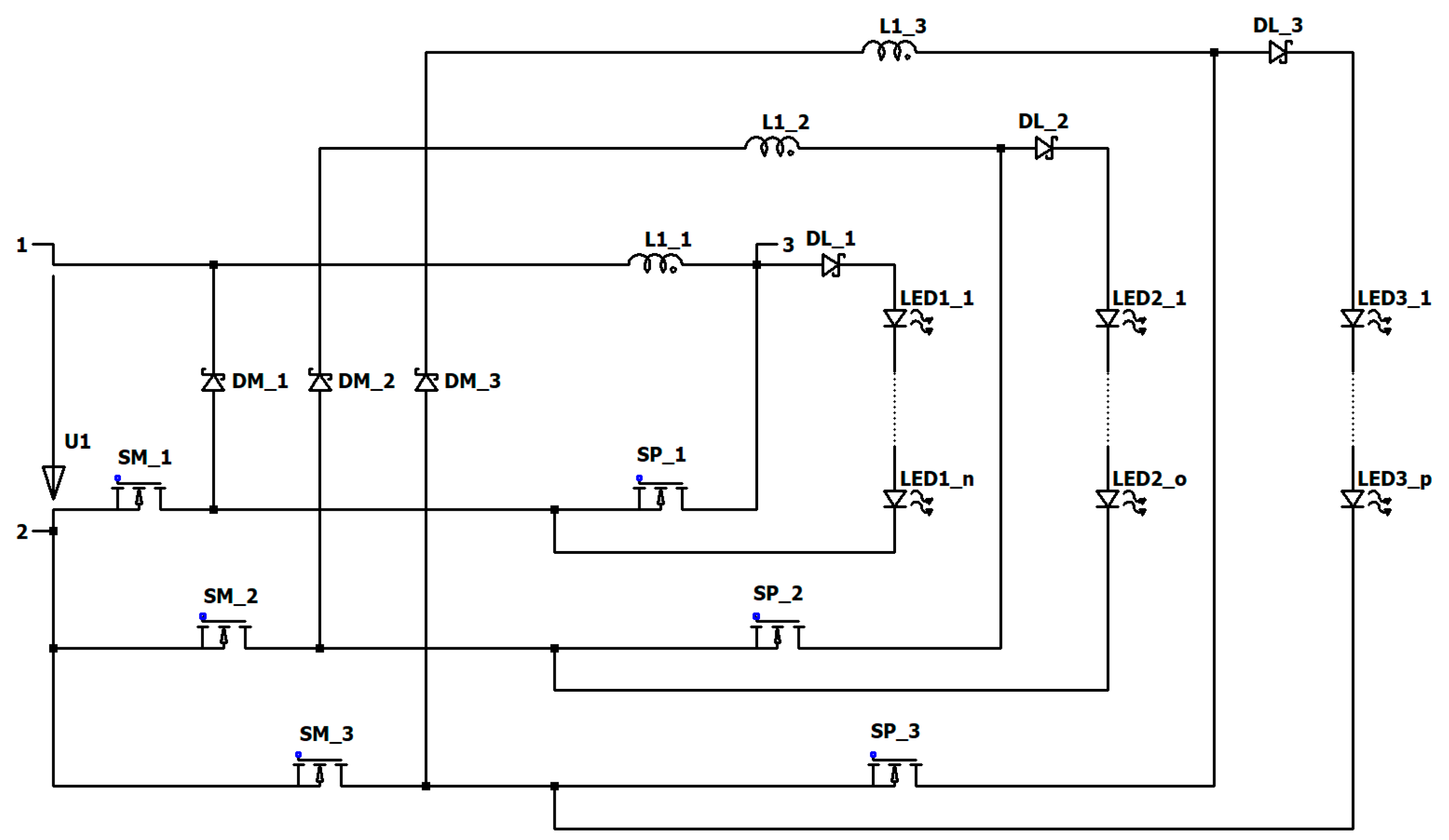
Another way to combine groups of LEDs radiating red, green, and blue light is shown in Figure 8. Three half-bridges consisting of a main switch SM and a pulse switch SP are used to control the three groups of LEDs. The half-bridges have the advantage that their parasitic inductance is very small.

2.3. Influence of the Parasitic Load Inductance

The load should be as near as possible to the output. This is not always possible and some parasitic inductance always occurs. Figure 9 shows the current through L1, the current through the load, the voltage across S2, and the voltage across S1. The parasitic inductance in series connection to the LEDs is 1 µH. When S2 turns off, the parasitic inductance produces a significant overvoltage across S2 and a short ringing of the current in the load occurs. With a small RC snubber, the overvoltage can be removed, as is also shown in Figure 9. With an additional RC snubber across the load (LEDs plus the series diode), a second modeled parasitic inductance can also be deactivated (Figure 10).
A further reduction is shown in Figure 10. Parallel to the LEDs, a second small RC snubber is connected (and the parasitic inductance is modeled by 1 µH in two different lines). It should be mentioned that 1 µH is relatively large.

3. Driving Stage II (Pulsed LED Driver with Half-Bridge)

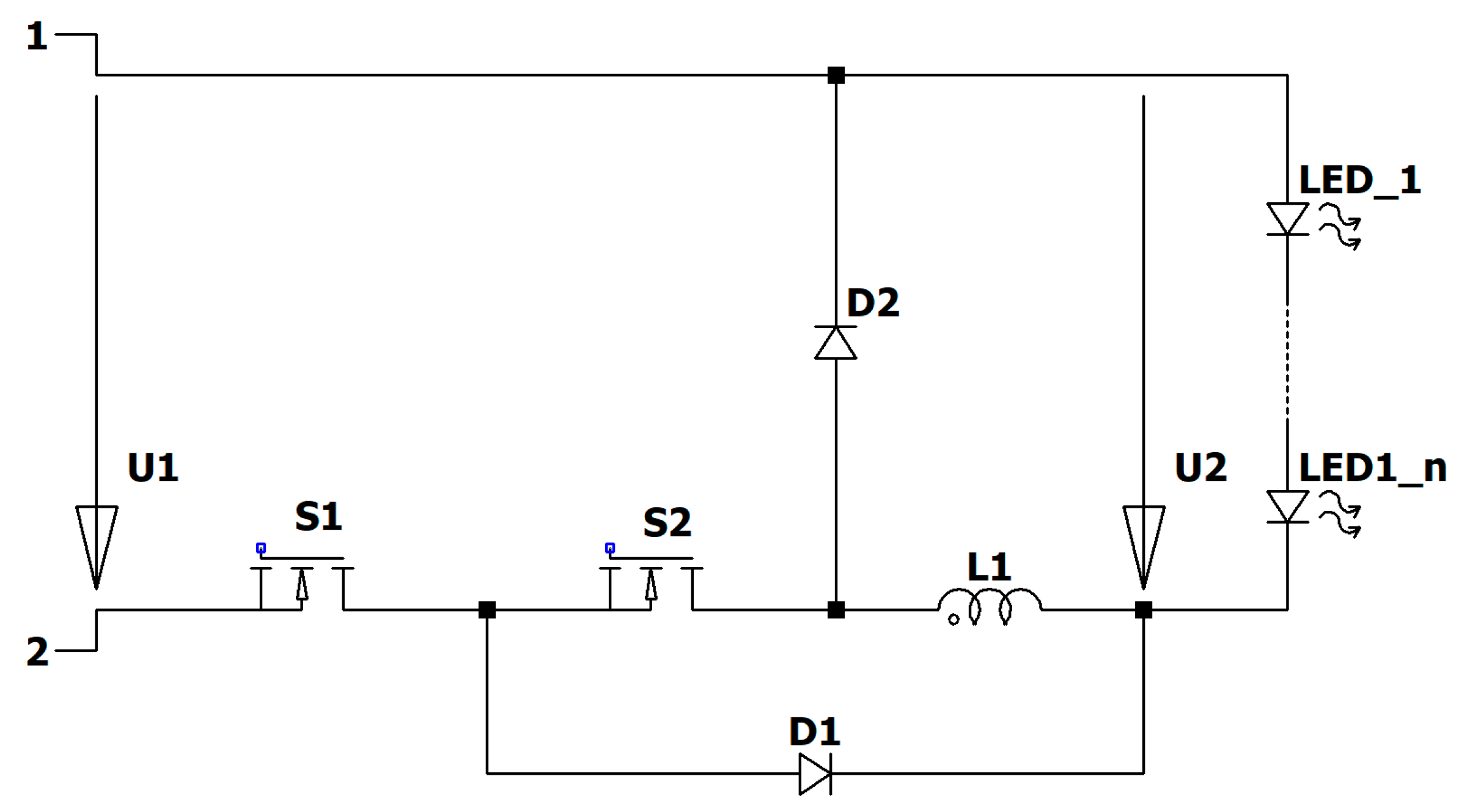
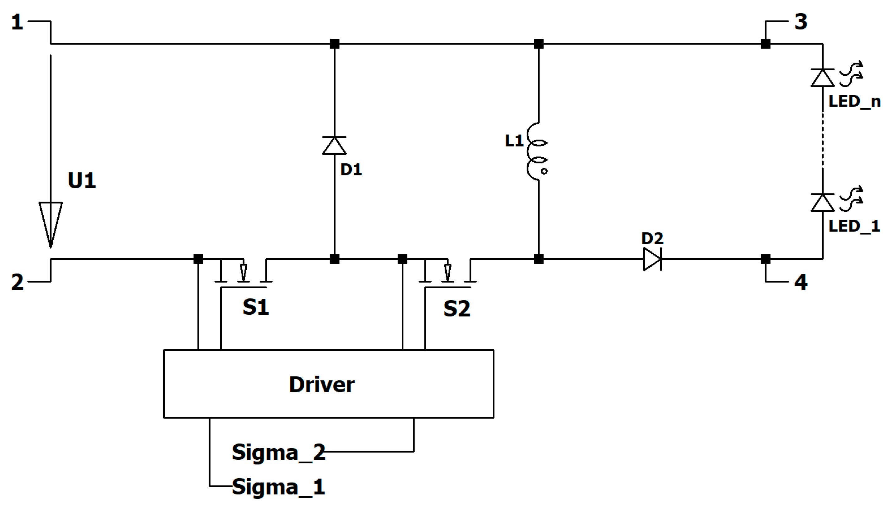
Another capacitor-free LED driver with the possibility to pulse the output is shown in Figure 11. It consists of two in-series connected electronic switches S1 and S2, two diodes D1 and D2, and an inductor L1. The input voltage is connected between the terminals 1 and 2. The load consists of the series connection from LED_1 to LED_n. This circuit has, again, the main advantage of needing no capacitor for the energy transformation. Only when the source of the input voltage is not directly connected does a small capacitor have to be connected between the negative pole of switch S1 and the cathode of D2 to avoid an overvoltage across the switches caused by the parasitic input inductance.
The driver has three modes in the continuous inductor current mode. During mode M1, both electronic switches S1 and S2 are on and both diodes are blocked. The current flows through the load, through L1, through the switches, and back to the input source U1. When S1 is turned off, the current through the inductor free-wheels through the diode D1. The current through the load is interrupted and the LEDs turn off. This is mode M2. Mode M3 starts when the active switch S2 is turned off, too. Now, D2 turns on and D1 turns off. The current through the inductor L1 free-wheels through diode D2 and the load. The information can now be transferred by the length of mode M2. During this mode, the light is turned off. When the current through L1 is controlled, the current can be held constant, and when mode M3 starts again, the current through the LEDs is the same as before during mode M1. A constant current through the LEDs causes a constant color temperature.
Modeling again the load by a crack characteristic, the current through the inductor during mode M1 is described by
d i L 1 d t = u 1 ( V L E D + R L E D · i L 1 ) L 1 .
The current increases linearly and when the current reaches the upper desired value, the electronic switch S1 is turned off. When no information has to be transmitted, the second electronic switch S2 is turned off, too. When information has to be transmitted, S2 stays on, the current through the coil turns on the diode D1, and the current free-wheels through S2 and D1 and stays nearly constant. Now, no current flows through the load and the LEDs are extinguished. When the electronic switch S2 is turned off, mode M3 begins and the current free-wheels through the diode D2 and the load. Now, the LEDs are turned on and produce light. The current through the inductor decreases according to the differential equation
d i L 1 d t = ( V L E D + R L E D · i L 1 ) L 1 .
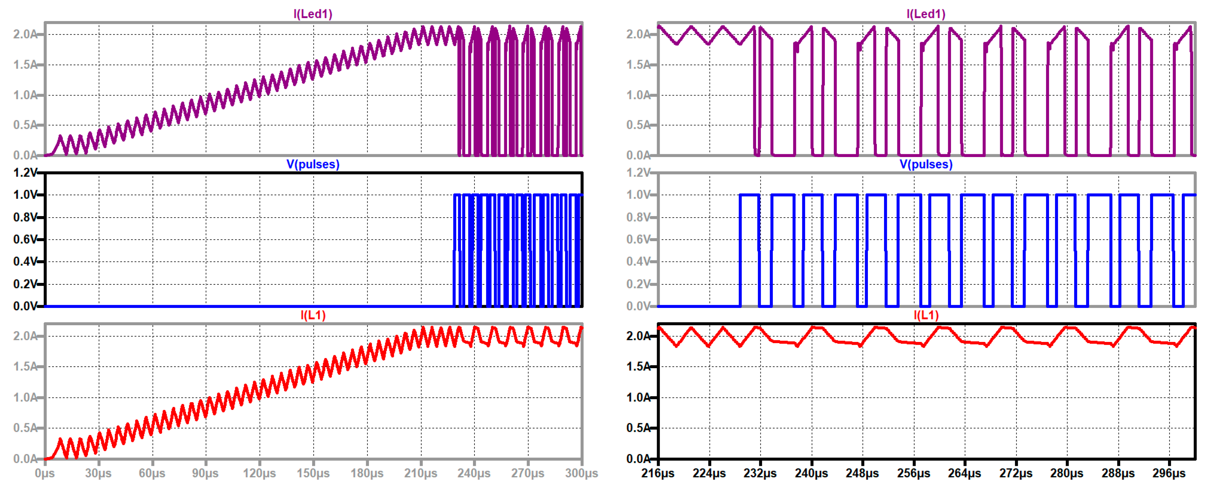
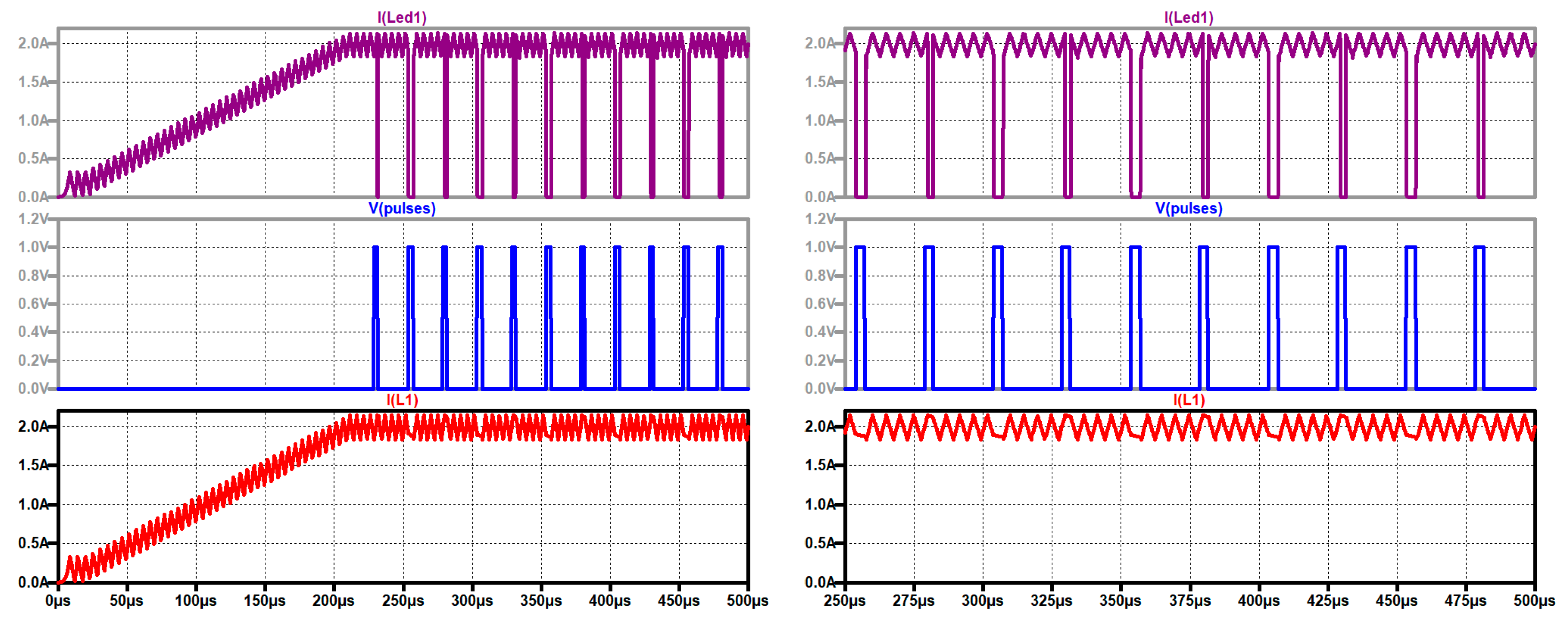
Figure 12 shows the current through the load, the control signal of S2, which carries the information over two different lengths, and the current through the inductor. On the left of the figure, the start-up is also shown; on the right side, the pulsing is shown enlarged. One can see the two different pulse lengths which bear the information. If the pulse lengths are only short, information telegrams are sent, e.g., eight bit, and then the next telegram is sent about eight pulses later, so the reduced illumination does not matter. When continuous information has to be sent, the current should be increased. The information should be formatted in such a way that the mean value of the current through the load should be constant.
Another way to maintain a constant current mean value through the load is by reducing the data rate. This is shown in Figure 13. Again, a little increase in the reference value can be made to keep the illumination constant.
To increase the data rate, each pulse is bearing information, as shown in Figure 14. The two switches must be synchronized and start at the same moment. The switching frequency and the data frequency are 500 kHz in Figure 14a and 1 MHz in Figure 14b. The current through the load, the control signal of the switches, and the current through the inductor are shown.
Figure 15 shows the combination of three converters to control groups of LEDs with the colors blue, red, and green. The control of each stage can be achieved through integrated half-bridge drivers with separate input signals. The supply voltage of the high-side driver is generated by a charge pump.

Influence of the Parasitic Output Inductance

Figure 16 shows the current through the load, the current through the coil, the data signal, and the control signal of S1, with a small parasitic inductance of 0.2 µH. Figure 16 also shows the voltage across S2, the voltage across S1, the current through the load, the current through the coil, the data signal, and the control signal of S1 without and with a small RC snubber of 10 Ω and 10 nF.

4. Driving Stage Type III

This driving stage for LEDs as shown in Figure 17, also needs no capacitor for the energy transformation and is more flexible concerning the input voltage, because it is based on the Buck–Boost converter. A peculiarity of this circuit is that the frequency of the data must be the same as the frequency of the converter. Again, the best way to control the current through the coil is by employing a hysteresis controller. Both active switches are turned on at the same time. When the current reaches the upper limit, the switch S1 is turned off. S2 is still on and the current through the coil commutates into the diode D1. When S2 is turned off, the current commutates into the load and the LEDs turn on. With two distinguishable turn-on times of S2, a digital signal can be produced; with three different turn-on times, a ternary logic is produced. The current through the load should be constant at the mean value.
The driving circuit consists of two active switches S1 and S2 and two diodes D1 and D2. Again, the circuit has three modes. During mode M1, both switches are turned on, the input voltage is across the inductor, and the current increases. The current through the coil changes according to
d i L 1 d t = u 1 L 1 .
When only S1 is turned off and S2 stays on, the current of the coil commutates into D1 and free-wheels. The voltage across the coil is now nearly zero. The small negative voltage is caused by the forward voltage of the diode plus the on-resistor of the active switch S2 and the parasitic resistor of the coil.
When S2 is turned off, the current commutates into the diode D2, the current of the coil flows through the load, and the illumination starts. The on-time of the LEDs depends on the off-time of the switch S2. With changes in the off-time of S2, information can be coded.
The inductor current changes now according to
d i L 1 d t = ( V L E D + R L E D · i L ) L 1 .
In VLED and RLED, not only the crack voltage of the LEDs and the differential resistor of the LEDs but also the crack voltage and the differential resistor of the diode D2 are included.
Using a hysteresis controller with the hysteresis ΔI, the duration of the on-time of the switch S1 is calculated as follows:
T o n = L 1 Δ I U 1 .
When no information has to be transmitted, S2 turns off after the same amount of time and the current decreases by ΔI during the same time, calculated as follows:
T o f f = L 1 Δ I V L E D + R L E D · I L 0 .
T o n + T o f f = L 1 Δ I 1 V L E D + R L E D · I L 0 + 1 U 1 = L 1 Δ I U 1 + V L E D + R L E D · I L 0 U 1 V L E D + R L E D · I L 0 .
The frequency of the hysteresis controller is therefore
f = U 1 V L E D + R L E D · I L 0 L 1 Δ I U 1 + V L E D + R L E D · I L 0 .
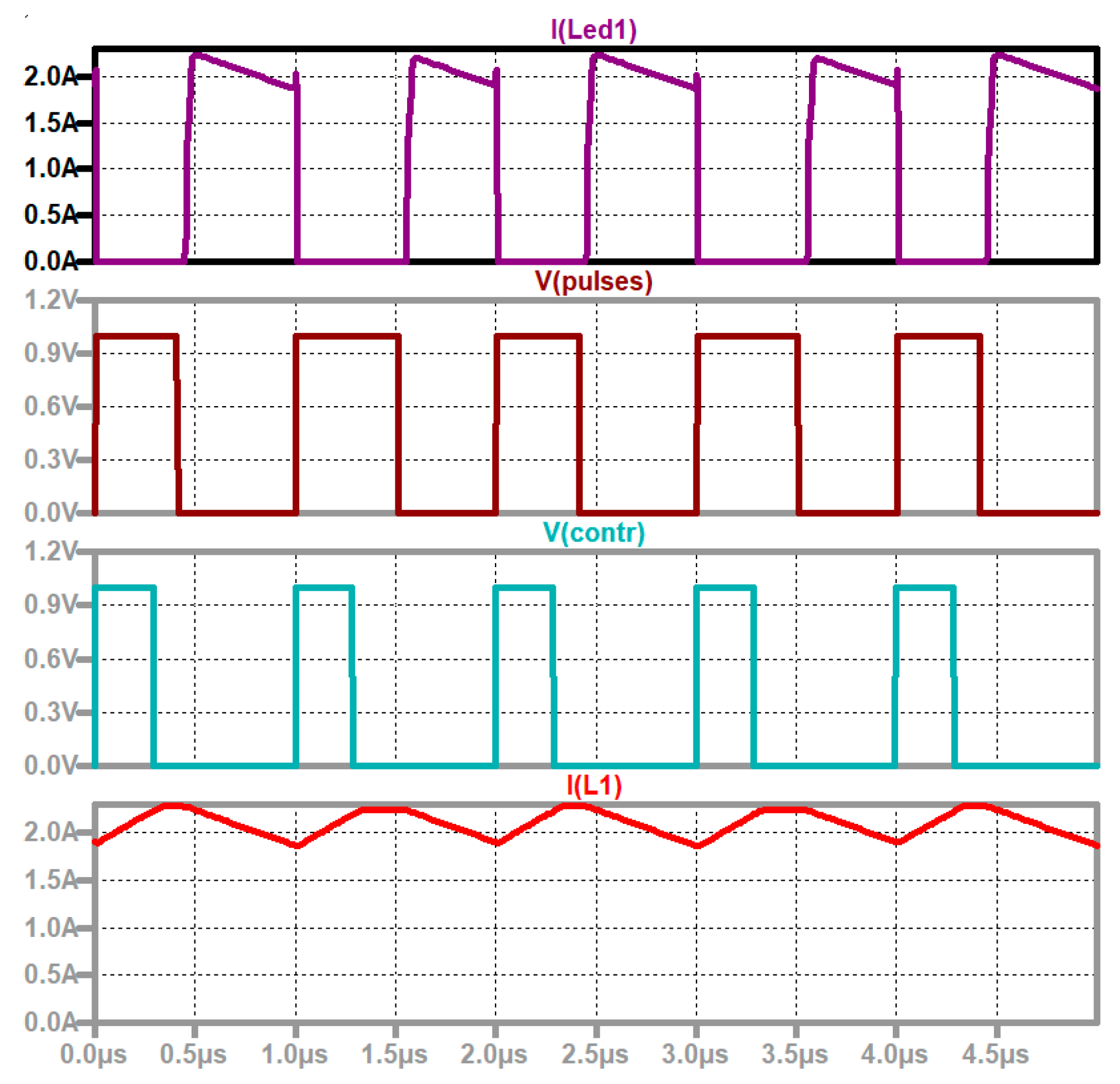
Figure 18 shows the current through the load, the pulses which contain the information, the control signal of the switch S1 which comes from the controller, and the current through the coil. The pulses change between two values which can be coded as high and low. The current increases when the signal “contr” is on, stays nearly constant during the time interval between the on-time of the “pulses” (this is the control signal of the switch S2) and the on-time of “contr” (this is the control signal of the switch S1), and decreases when the switch S2 is turned off.
To achieve the same mean value of the current through the LEDs, the current through the coil must be higher than the mean value of the current through the LEDs. Figure 19 shows the same signals, but the current through the coil is controlled to have a certain value so that the desired current flows through the LEDs at the same mean value.

4.1. Hysteresis Controller

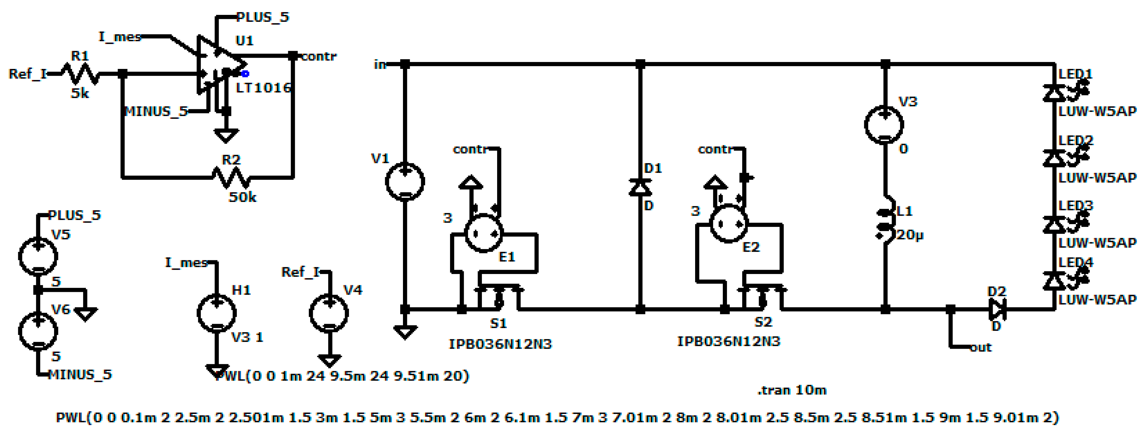
The simulation circuit of the driver of type III with a hysteresis controller is depicted in Figure 20. The current through the coil is measured by the current through the voltage source V3 and transformed into a voltage by the current-controlled voltage source H1. The voltage I_mes is compared with the reference value Ref_I by the comparator U1. The hysteresis is adjusted by the resistors R1 and R2. The output signal of the controller contr is amplified by the voltage-controlled voltage sources E1 and E2, which are connected to the gate and source of the electronic switches.
Figure 21 shows the behavior of the hysteresis controller. The reference value, the input voltage, and the current through the coil are shown. The current follows the reference value and the changes in the input voltage do not disturb.
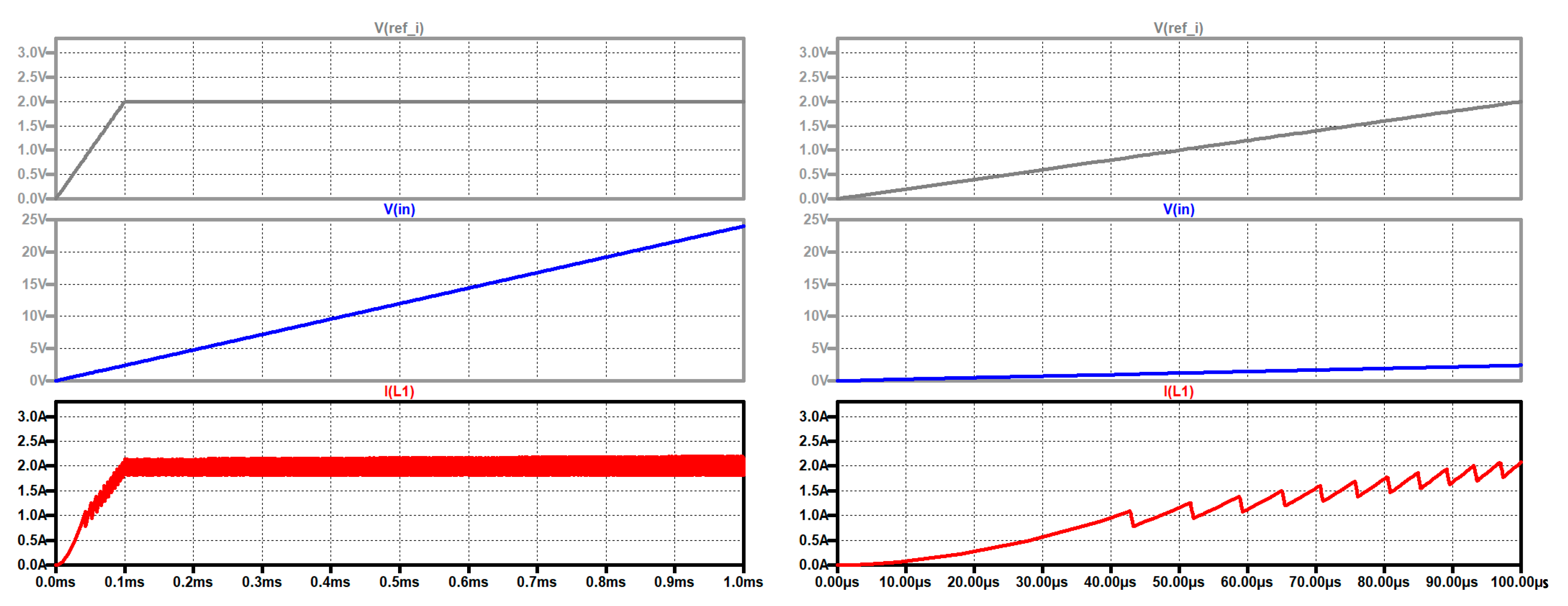
Figure 22 shows the start-up. The input voltage increases and so does the reference value. The current follows the reference value even when the voltage is low. The frequency of the controller is now also low.
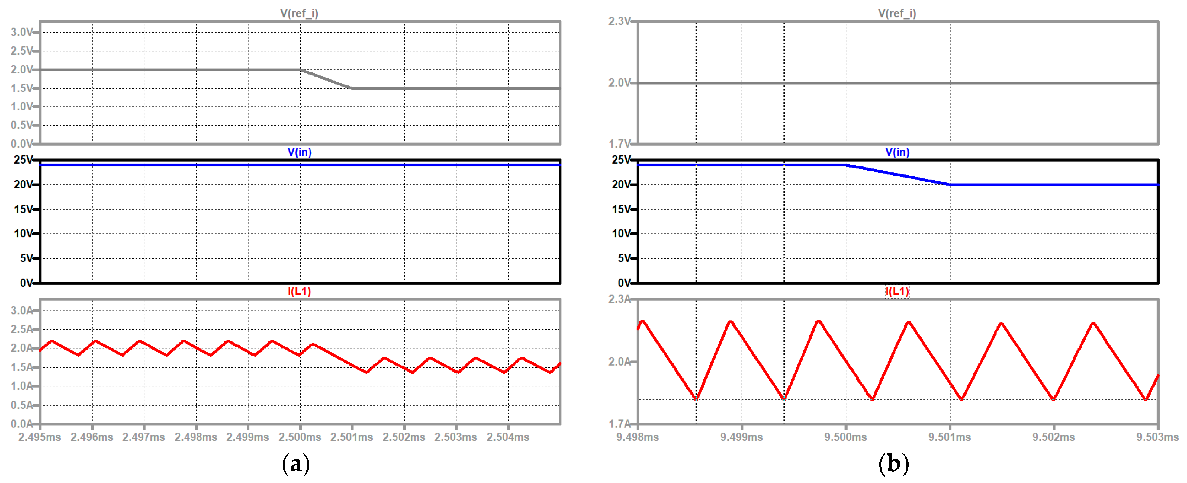
The controller reacts immediately to changes in the reference value and the input voltage. Figure 23a shows a step of the reference value within 1 µs. The current follows and the frequency changes from 1.18 MHz to 0.89 MHz. Figure 23b shows a step of the input voltage within 1 µs, where the current stays constant.
Figure 24 shows an extended version where the group of LEDs can be short-circuited. So, with red, green, and blue LEDs, the chrominance can be changed and the data can now be sent through three channels.

4.2. Influence of the Parasitic Inductance at the Load Side

Figure 25 shows the influence of the parasitic inductance of the load. Ringing occurs during mode M3. The ripple current through the coil, the voltage across the load, the voltage across S2, the voltage across S1, and the input voltage are depicted.
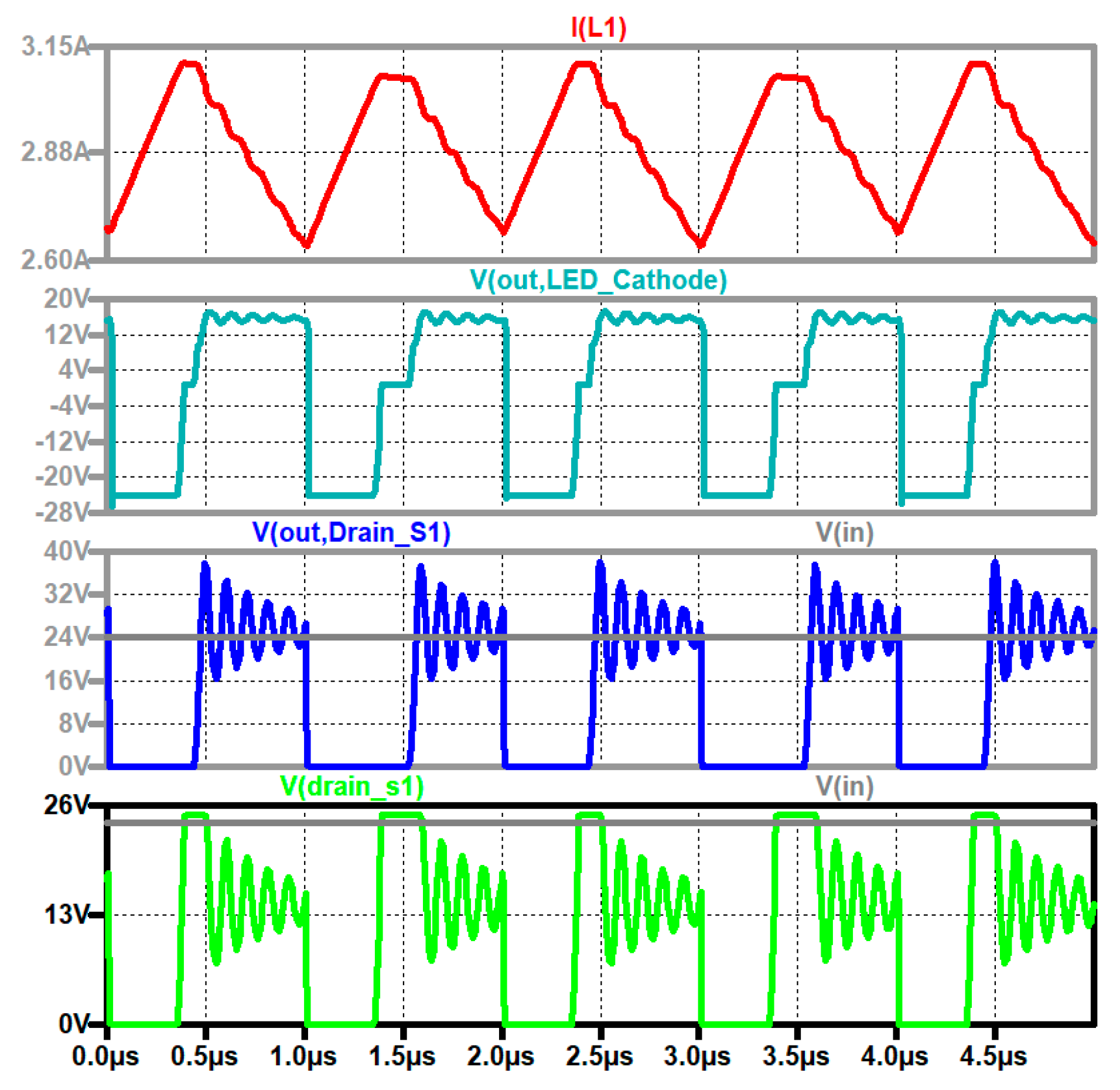
The load (LEDs) and the diode D2 should be connected as near as possible to the coil L1 to avoid the overvoltage. Figure 26 shows the ripple current through L1, the voltage across the load, the voltage across S2 (gray), and the voltage across S1. The straight line in the bottom two graphs is the input voltage. The parasitic inductance has the value 0.2 µH. When the switches are off, a pronounced ringing of the voltage occurs across them. To avoid this ringing, a small RC snubber (10 Ω in series with 10 nF) is connected across the second active switch S2. The time constant of the snubber is near to the period of the ringing.

5. Combination of Three Converters

Figure 27 shows a combination of three converters building a single-input multiple-output system. The current of each coil is again controlled by a hysteresis controller. When the groups of LEDs have the colors red, blue, and green, the chrominance and the color temperature can be changed, and with three equivalent photodetectors, one can now send information through three channels.

6. Further Aspects

It should be mentioned first that these considerations are also valid for all three circuits.

6.1. Influence of the Parasitic Input Inductance

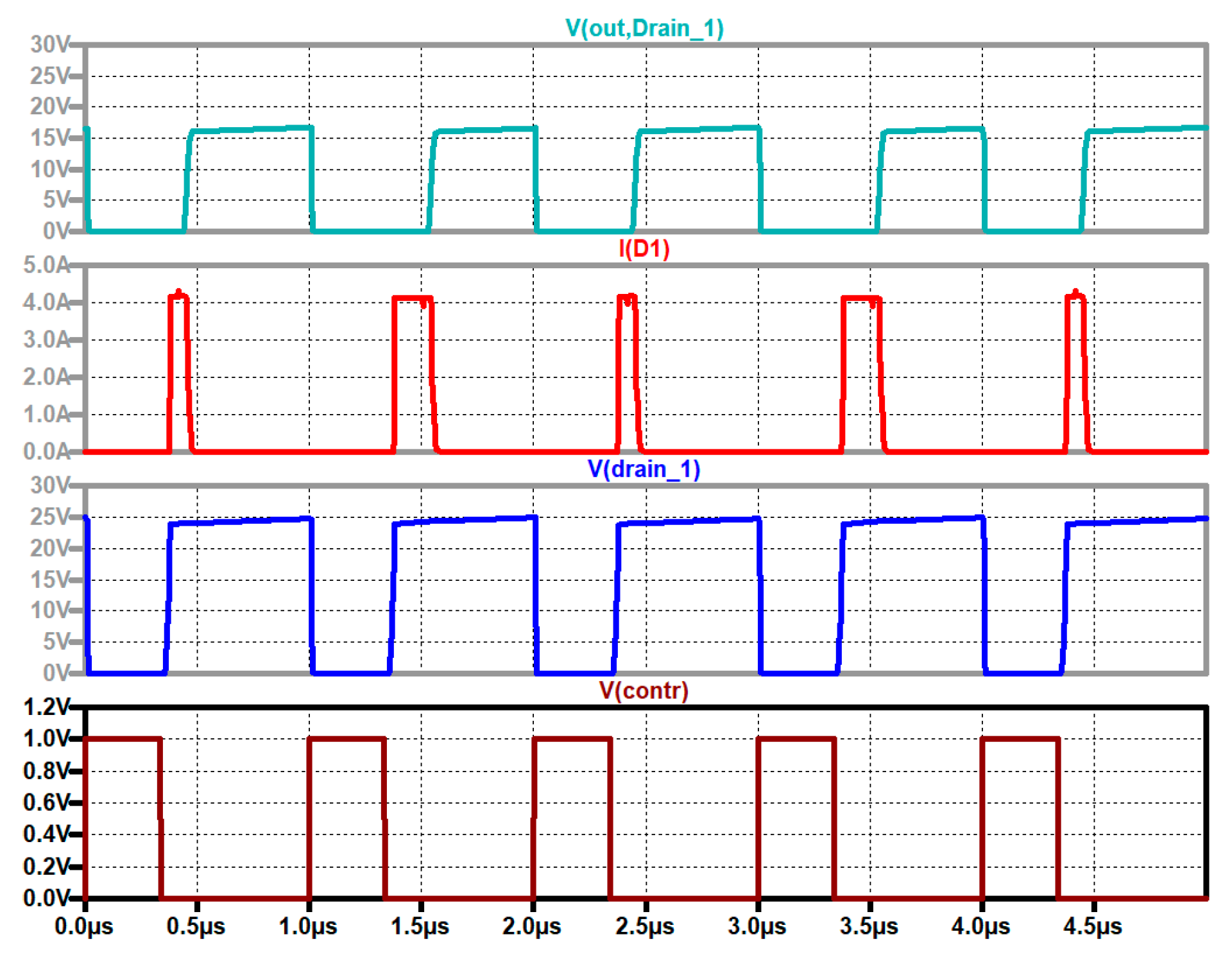
The input source should be an ideal voltage source, e.g., a DC microgrid. The converter is connected by wires to the source. The parasitic inductance leads to a high overvoltage across the switch S1. To avoid the overvoltage, a small capacitor must be connected between the cathode of D1 and the negative terminal of the switch S1. Figure 28 shows the effect of a 470 nF capacitor in the interplay with a typical parasitic inductance of 1 µH. The overvoltage is suppressed.

6.2. Dimming

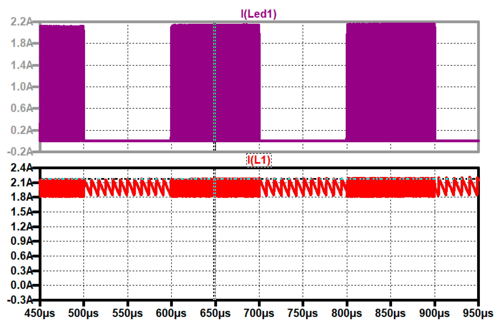
There are two possibilities to dim the radiation. First, one can reduce the reference value of the current through the coil, and second, one can reduce the frequency. The second concept has the advantage that the LEDs radiate with a constant color temperature and the light pulses have the same amplitude. This is advantageous for the data receiver. Figure 29 shows the dimming signal, the current through the load, and the current through the coil. The current through the coil is controlled to be 2 A. The frequency during turn off is 117 kHz, and during lighting, it is 1.05 MHz.

7. Conclusions

This paper presents three LED drivers which have some interesting features and can be used for illumination and simultaneous data transmission. No large capacitors are necessary, so the circuits are compact and cheap. There is no inrush current when connected to a stable input supply. The simple control concept is realized with a hysteresis current controller. A small capacitor, to avoid an overvoltage across the active switch caused by the input inductor of the wiring of the supply voltage, is necessary. Only a small RC snubber, with a very small capacitor, may be necessary when the load is not directly connected. By using red, green, and blue LEDs, the chrominance can be controlled and three data channels can be used. Furthermore, dimming is easily possible. A future research topic can be to extend the converters to multi-stage systems, as briefly suggested in this paper. This can easily be achieved by adopting single-phase systems. In this context, investigating the control of the chrominance and color temperature could be a potential field of research. The converters can be easily extended to multi-stage systems. There are various interesting real-world applications of the proposed system. The LED driving converters can be used for illumination combined with data transmission. This could be applied for indoor and outdoor applications, such as in the home, in industry, and for office solutions. Promising topics are illumination, vehicles, autonomous cars, traffic signs, railways, automotive applications, robotics, maritime applications, medicine, and many more possible application cases.

Author Contributions

Conceptualization, M.W. and F.A.H.; writing, M.W. and F.A.H.; simulation, M.W. and F.A.H.; validation, M.W. and F.A.H.; writing—original draft preparation, H.L.V.; writing—review and editing, M.W., F.A.H. and H.L.V.; visualization, F.A.H.; supervision, F.A.H., H.L.V., M.L. and O.S. All authors have read and agreed to the published version of the manuscript.

Funding

This research received no external funding.

Institutional Review Board Statement

Not applicable.

Informed Consent Statement

Not applicable.

Data Availability Statement

No new data were created or analyzed in this study. Data sharing is not applicable to this article.

Acknowledgments

Open Access Funding by the University of Applied Sciences Technikum Wien.

Conflicts of Interest

The authors declare no conflict of interest.

References

  1. Céspedes, M.M.; Guzmán, B.G.; Jiménez, V.P.G.; Armada, A.G. Aligning the Light for Vehicular Visible Light Communications: High Data Rate and Low-Latency Vehicular Visible Light Communications Implementing Blind Interference Alignment. IEEE Veh. Technol. Mag. 2023, 18, 59–69. [Google Scholar] [CrossRef]
  2. Younus, S.H.; Al-Hameed, A.A.; Hussein, A.T.; Alresheedi, M.T.; Elmirghani, J.M.H. Parallel Data Transmission in Indoor Visible Light Communication Systems. IEEE Access 2019, 7, 1126–1138. [Google Scholar] [CrossRef]
  3. You, X.; Chen, J.; Zheng, H.; Yu, C. Efficient Data Transmission Using MPPM Dimming Control in Indoor Visible Light Communication. IEEE Photonics J. 2015, 7, 7902512. [Google Scholar] [CrossRef]
  4. Xie, E.; Chen, C.; Ouyang, C.; Hill, J.; McKendry, J.J.; Zhang, Y.; Gu, E.; Herrnsdorf, J.; Haas, H.; Dawson, M.D. GaN-Based Series Hybrid LED Array: A Dual-Function Light Source With Illumination and High-Speed Visible Light Communication Capabilities. J. Light Technol. 2024, 42, 243–250. [Google Scholar] [CrossRef]
  5. Ntogari, G.; Kamalakis, T.; Walewski, J.; Sphicopoulos, T. Combining Illumination Dimming Based on Pulse-Width Modulation with Visible-Light Communications Based on Discrete Multitone. J. Opt. Commun. Netw. 2011, 3, 56–65. [Google Scholar] [CrossRef]
  6. Xiao, H.; Xiao, X.; Wang, K.; Wang, R.; Xie, B.; Chiang, K.S. Optimization of Illumination Performance of Trichromatic White Light-Emitting Diode and Characterization of Its Modulation Bandwidth for Communication Applications. IEEE Photonics J. 2018, 10, 8201511. [Google Scholar] [CrossRef]
  7. Chun, H.; Chiang, C.-J.; Monkman, A.; O’Brien, D. A Study of Illumination and Communication using Organic Light Emitting Diodes. J. Light Technol. 2013, 31, 3511–3517. [Google Scholar] [CrossRef]
  8. Edelmoser, K.H.; Himmelstoss, F.A. High Dynamic Current Source for LED Light and Data Transmission Applications. In Proceedings of the International Exhibition and Conference for Power Electronics, Intelligent Motion, Renewable Energy and Energy Management, Nuremberg, Germany, 28–30 June 2016; pp. 1–8, PCIM Europe 2016. [Google Scholar]
  9. Morales-Céspedes, M. Interference Management in Visible Light Communications based on Reconfigurable Photodetectors for Industrial IoT. In Proceedings of the 2023 IEEE International Workshop on Metrology for Industry 4.0 & IoT (MetroInd4.0 & IoT), Brescia, Italy, 6–8 June 2023; pp. 376–381. [Google Scholar] [CrossRef]
  10. Heinig, S.; Jacobs, K.; Norrga, S.; Nee, H.-P. Single-Fiber Combined Optical Power and Data Transmission for High-Voltage Applications. In Proceedings of the IECON 2020 The 46th Annual Conference of the IEEE Industrial Electronics Society, Singapore, 18–21 October 2020; pp. 1473–1480. [Google Scholar] [CrossRef]
  11. Pawlikowski, W.; Barmaki, A.; Narimani, M.; Hranilovic, S. Light-Emitting Commutating Diodes for Optical Wireless Communications within LED Drivers. IEEE Photonics J. 2020, 12, 7905111. [Google Scholar] [CrossRef]
  12. Soundari, D.V.; Varshini, G.; Vijayalakshmi, G. Development of V2V Communication using Light Fidelity. In Proceedings of the 2022 3rd International Conference on Electronics and Sustainable Communication Systems (ICESC), Coimbatore, India, 17–19 August 2022; pp. 565–568. [Google Scholar] [CrossRef]
  13. Sangmahamad, P.; Pirajnanchai, V.; Junon, S. Experimental Validation and Performance Analysis for Simultaneous Illumination and Communication System of Indoor Commercial white-LED Lamps. In Proceedings of the 2021 13th International Conference on Information Technology and Electrical Engineering (ICITEE), Chiang Mai, Thailand, 14–15 October 2021; pp. 30–33. [Google Scholar] [CrossRef]
  14. Wang, C.; Zou, P.; Chen, J.; Li, G.; Chi, N. Internet of Vehicle System Based on Automotive Headlight utilizing Probabilistic Shaping. In Proceedings of the 2019 11th International Conference on Wireless Communications and Signal Processing (WCSP), Xi’an, China, 23–25 October 2019; pp. 1–4. [Google Scholar] [CrossRef]
  15. Deng, P.; Kavehrad, M. Real-time software-defined single-carrier QAM mimo visible light communication system. In Proceedings of the 2016 Integrated Communications Navigation and Surveillance (ICNS), Herndon, VA, USA, 19–21 April 2016; pp. 5A3-1–5A3-11. [Google Scholar] [CrossRef]
  16. Chen, Y.; Chang, C.; Yang, P. A novel constant current control circuit for a primary-side controlled AC-DC LED driver. In Proceedings of the 2014 11th International Conference on Electronics, Computer and Computation (ICECCO), Abuja, Nigeria, 29 September–1 October 2014; pp. 1–4. [Google Scholar] [CrossRef]
  17. Shan, Z.; Chen, X.; Fan, S.; Yuan, G.; Tse, C.K. Resonant Switched-capacitor Auxiliary Circuit for Active Power Decoupling in Electrolytic Capacitor-less AC/DC LED Drivers. In Proceedings of the 2019 IEEE Energy Conversion Congress and Exposition (ECCE), Baltimore, MD, USA, 29 September–3 October 2019; pp. 866–871. [Google Scholar] [CrossRef]
  18. Yu, J.; Zhou, J. A Multi-Channel Low-Power LED Driver Circuit for PPG. In Proceedings of the 2023 IEEE 17th International Conference on Anti-counterfeiting, Security, and Identification (ASID), Xiamen, China, 1–3 December 2023; pp. 12–15. [Google Scholar] [CrossRef]
  19. Pham-Nguyen, L.; Nguyen, V.-Q.; Nguyen, D.-M.; Han, H.-D.; Nguyen, K.-H.; Le, H.-P. A 14-W 94%-Efficient Hybrid DC-DC Converter with Advanced Bootstrap Gate Drivers for Smart Home LED Applications. In Proceedings of the 2018 IEEE Energy Conversion Congress and Exposition (ECCE), Portland, OR, USA, 23–27 September 2018; pp. 4744–4749. [Google Scholar] [CrossRef]
  20. Pallapati, R.B.; Chinthamalla, R.; Reddy, S.S.; Mishra, S.; Bommu, H.V. Reduced Power Processing Constant Output Current High Efficient Electrolytic Capacitor-less Single Phase LED Driver. In Proceedings of the 2023 IEEE 3rd International Conference on Smart Technologies for Power, Energy and Control (STPEC), Bhubaneswar, India, 10–13 December 2023; pp. 1–6. [Google Scholar] [CrossRef]
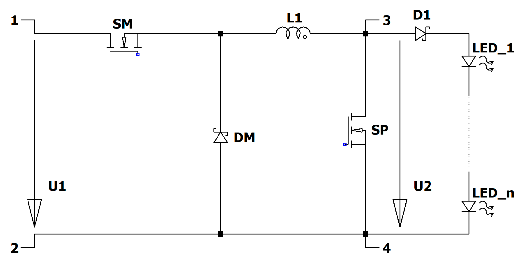
Figure 1. The basic structure of the LED driver of type I with the possibility to pulse the output.
Electricity 05 00016 g001
Figure 2. The simulation circuit. From top to bottom: the control signal of the pulsing switch (turquoise), the control signal of the main switch (blue), the load current (violet), the current through the coil (red), and the change in the current through the coil (red).
Electricity 05 00016 g002
Figure 3. The simulation circuit. From top to bottom: the control signal of the pulsing switch (turquoise), the control signal of the main switch (blue), the load current (violet), the current through the coil (red), and the change in the current through the coil (red).
Electricity 05 00016 g003
Figure 4. From top to bottom: the input voltage (green); the control signal of the pulsing switch (turquoise); the control signal of the main switch (blue); the load current (violet); the current through the coil (red); the change in the current through the coil (red).
Electricity 05 00016 g004
Figure 5. Simulation circuit.
Electricity 05 00016 g005
Figure 6. From top to bottom: current through LED3 (brown), current through LED2 (violet), current through LED1 (dark violet), control signal of main switch (dark blue), control signal of LED3 (turquoise), control signal of LED2 (blue), control signal of LED1 (green), and change in current through coil (red).
Electricity 05 00016 g006
Figure 7. (a) First variation. (b) Second variation.
Electricity 05 00016 g007
Figure 8. Combination of three converters of type I.
Electricity 05 00016 g008
Figure 9. Influence of parasitic load inductance. From top to bottom: ripple current through L1 (red), current through load (dark violet), voltage across S2 (blue), control signal of S2 (turquoise), voltage across S1 (green), and parasitic load inductance 1 µH without and with RC snubber of 10 Ω and 10 nF across S2.
Electricity 05 00016 g009
Figure 10. From top to bottom: ripple current through L1 (red), current through load (dark violet), voltage across S2 (blue), control signal of S2 (turquoise), voltage across S1 (green), and parasitic load inductance of 1 µH twice with RC snubber with 10 Ω and 10 nF across S2 and across load.
Electricity 05 00016 g010
Figure 11. Driving stage II.
Electricity 05 00016 g011
Figure 12. Start-up and pulsing information. From top to bottom: the current through the LEDs (dark violet), the information (blue), and the current through the coil (red).
Electricity 05 00016 g012
Figure 13. Start-up and pulsing information. From top to bottom: the current through the LEDs (dark violet), the information (blue), and the current through the coil (red).
Electricity 05 00016 g013
Figure 14. (a) A clock frequency of 500 kHz. From top to bottom: the current through the load (dark violet); the control signal of S2 (black); the control signal of S1 (turquoise); the current through the inductor (red). (b) A clock frequency of 1 MHz. From top to bottom: the current through the load (dark violet); the control signal of S2 (black); the control signal of S1 (turquoise); the current through the inductor (red).
Electricity 05 00016 g014aElectricity 05 00016 g014b
Figure 15. Combination of three LED drivers of type II.
Electricity 05 00016 g015
Figure 16. With parasitic inductance of 0.2 µH, from top to bottom: voltage across S2 (dark green); voltage across S1 (turquoise); current through load (dark violet); current through coil (red); data (blue); control signal of S1 (green), without and with snubber in parallel to S2.
Electricity 05 00016 g016
Figure 17. LED driver and pulser of type III.
Electricity 05 00016 g017
Figure 18. The current through the coil measuring at 2 A. From top to bottom: the current through the load (dark violet); pulses (black); the control signal of the switch S1 (turquoise); the current through the coil (red).
Electricity 05 00016 g018
Figure 19. A current through the coil measuring at 2 A. From top to bottom: the current through the load (dark violet); pulses (black); the control signal of the switch S1 (turquoise); the current through the coil (red).
Electricity 05 00016 g019
Figure 20. Simulation circuit of hysteresis-controlled driving stage of type III.
Electricity 05 00016 g020
Figure 21. Hysteresis-controlled driving stage of type III. From top to bottom: reference value (gray), input voltage (blue), and current through coil (red).
Electricity 05 00016 g021
Figure 22. Start-up of hysteresis-controlled driving stage of type III. From top to bottom: reference value (gray), input voltage (blue), and current through coil (red).
Electricity 05 00016 g022
Figure 23. Hysteresis-controlled driving stage of type III: (a) reference value step; (b) input voltage step. From top to bottom: reference value (gray), input voltage (blue), and current through coil (red).
Electricity 05 00016 g023
Figure 24. Extended version of type III.
Electricity 05 00016 g024
Figure 25. Hysteresis-controlled driving stage of type III: influence of parasitic inductor at load side with 0.2 µH and 0.2 Ω. From top to bottom: current through L1 (red); voltage across load (turquoise); voltage across S2 (blue); input voltage (gray); voltage across S1 (green); input voltage (gray).
Electricity 05 00016 g025
Figure 26. Hysteresis-controlled driving stage of type III: influence of parasitic inductor at load side with 0.2 µH and 0.2 Ω and with RC snubber 10 Ω + 10 nF. From top to bottom: current through L1 (red); voltage across load (turquoise); voltage across S2 (blue); input voltage (gray); voltage across S1 (green); input voltage (gray).
Electricity 05 00016 g026
Figure 27. Combination of three driving stages of type III.
Electricity 05 00016 g027
Figure 28. The removal of the influence of the parasitic inductance at the input side. From top to bottom: the voltage across S1 (turquoise); the current through D1 (red); the voltage across S1 (blue); the control signal of S1 (black). The parasitic inductance is 1 µH and 470 nF is used as the input capacitor.
Electricity 05 00016 g028
Figure 29. Dimming, from top to bottom: current through LEDs (dark violet); current through L1 (red).
Electricity 05 00016 g029
Disclaimer/Publisher’s Note: The statements, opinions and data contained in all publications are solely those of the individual author(s) and contributor(s) and not of MDPI and/or the editor(s). MDPI and/or the editor(s) disclaim responsibility for any injury to people or property resulting from any ideas, methods, instructions or products referred to in the content.