Abstract
This article presents the development and execution of a Single-Ended Primary-Inductor Converter (SEPIC) multiplier within a Hardware-in-the-Loop (HIL) emulation environment tailored for photovoltaic (PV) applications. Utilizing the advanced capabilities of the dSPACE 1104 platform, this work establishes a dynamic data exchange mechanism between a variable voltage power supply and the SEPIC multiplier converter, enhancing the efficiency of solar energy harnessing. The proposed emulation model was crafted to simulate real-world solar energy capture, facilitating the evaluation of control strategies under laboratory conditions. By emulating realistic operational scenarios, this approach significantly accelerates the innovation cycle for PV system technologies, enabling faster validation and refinement of emerging solutions. The SEPIC multiplier converter is a new topology based on the traditional SEPIC with the capability of producing a larger output voltage in a scalable manner. This initiative sets a new benchmark for conducting PV system research, offering a blend of precision and flexibility in testing supervisory strategies, thereby streamlining the path toward technological advancements in solar energy utilization.
1. Introduction
The growing concern over the exacerbation of the greenhouse effect, primarily attributed to the significant emissions of pollutants from human activities, has been a driving force behind the innovation of new models for energy generation [1,2,3,4]. This imperative has led to the development and implementation of renewable energy systems, including solar photovoltaic (PV), wind, hydraulic, and geothermal power systems, aimed at curtailing our dependency on fossil fuels and other non-renewable resources [4,5,6].
At the forefront of these advancements in power electronics is the strategic elimination of traditional fieldwork requirements. This objective is realized through the deployment of sophisticated emulation systems designed to replicate the dynamics of real-world power systems accurately. Such systems incorporate the precise characteristics of the energy systems under study, including the simulation of environmental atmospheric conditions. The adoption of these emulation techniques not only enhances the accuracy of energy system evaluations but also significantly contributes to the refinement of power generation technologies by providing a controlled yet realistic environment for testing and optimization. By leveraging these advanced emulation platforms, researchers and engineers are equipped with the tools necessary to conduct comprehensive analyses, thereby accelerating the development and adoption of efficient and sustainable energy solutions [7,8,9,10,11].
The employment of Hardware-in-the-Loop (HIL) simulation stands as a cornerstone in the realm of control systems testing, offering an innovative avenue for rigorous evaluation within a controlled virtual setting before establishing a direct interface with the actual converter. This methodology markedly diminishes the temporal and logistical demands traditionally associated with the setup and execution of empirical trials and validations using tangible hardware components. Presently, the integration of advanced simulation platforms equipped with high-performance multicore processors empowers researchers and engineers to meticulously design and test complex systems. These platforms enable the construction and manipulation of detailed virtual models, thereby accelerating the development process without compromising the fidelity or accuracy of the outcomes. The strategic utilization of HIL simulation not only streamlines the research and development cycle but also enhances the precision and reliability of the system under test, ensuring that results are both swift and precise [10,11,12,13,14].
Although solar panel emulation systems are available on the market [15,16], they are developed around closed (non-customizable by the user) platforms that do not allow for simple experimentation with different power electronics-based conversion systems. Programmable sources, such as those offered by CHROMA, are expensive compared to laboratory prototypes that can maximize the flexibility of emulating solar panel modules and the conversion systems used to implement MPPT algorithms.
This paper posits the utilization of Power Hardware-in-the-Loop (PHIL) simulation as a transformative approach for the integration of a DC/DC Single-Ended Primary-Inductor Converter (SEPIC) multiplier converter within a solar panel emulation framework managed by an advanced Maximum Power Point Tracking (MPPT) algorithm. An improved version of the work preliminarily introduced in [17], the proposed system aims to optimize power extraction, thereby enhancing the overall efficiency and reliability of photovoltaic systems. The SEPIC multiplier converter is a recently introduced and studied topology which can provide a larger voltage gain according to the number of diodes and capacitors added to the topology.
PHIL simulation facilitates a detailed and realistic emulation of solar energy systems, allowing for the thorough investigation and refinement of control strategies to ensure maximum energy yield and system performance. Through this approach, the research endeavors to bridge the gap between theoretical models and practical applications, fostering the development of more efficient and sustainable renewable energy solutions.
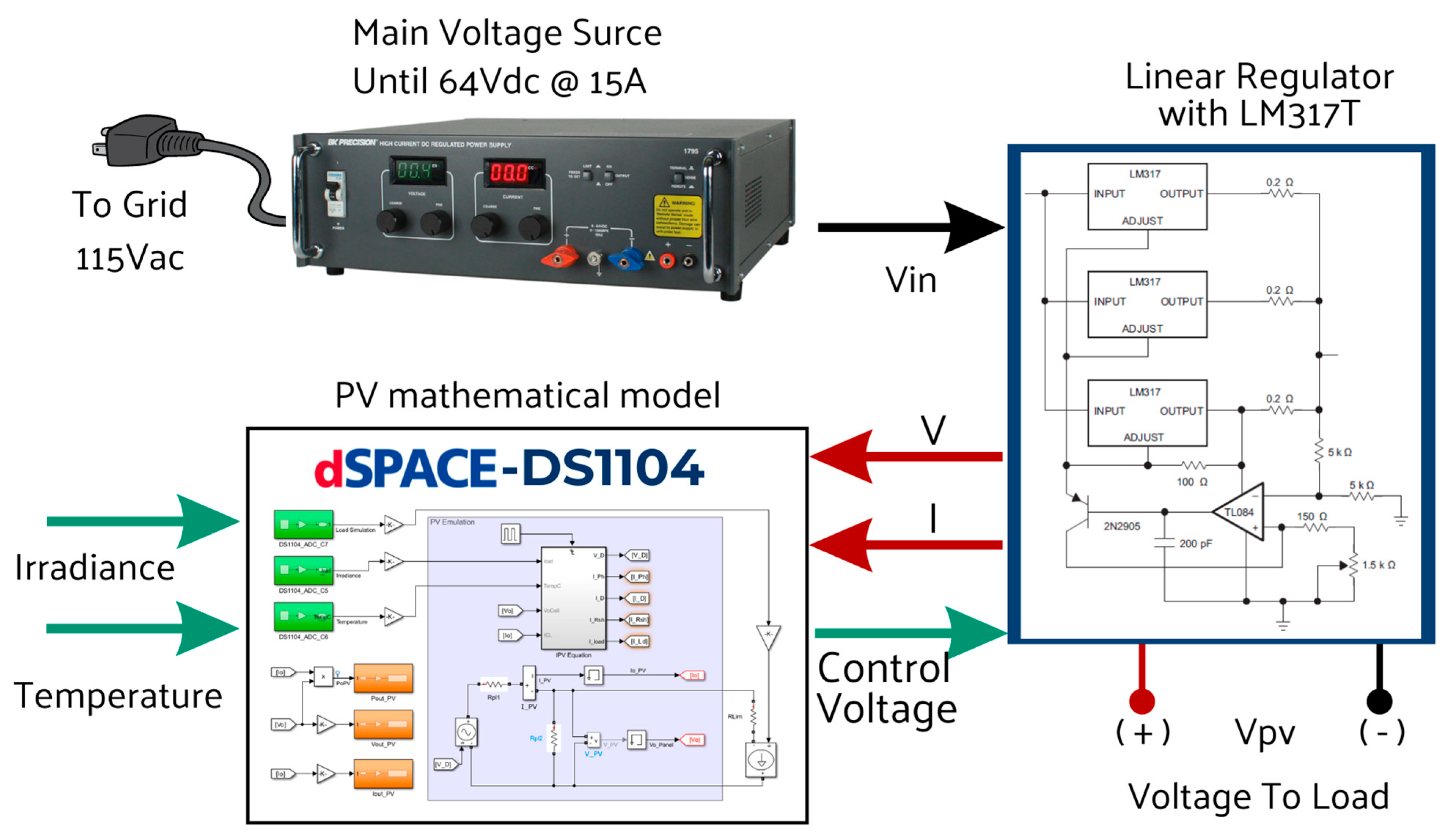
The PHIL system implemented in this work has the DS1104 data acquisition system from dSPACE as its central element. The DS1104 is a comprehensive data acquisition and processing card. With the aid of Matlab-Simulink – R2023b, detailed models can be created, which are then programmed on the DS1104. The general scheme of the data acquisition system is shown in Figure 1, where the software–hardware interaction that allows the emulation of the system is schematized. While the mathematical models are digitally processed in the DAQ system (DS1104), the output variables, voltages, currents, and powers are amplified by an electronic power source. At the same time, the voltages entering the model—the external command signals—are integrated into the process through the analog inputs of the DS1104 system.
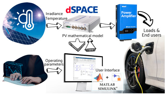
Figure 1.
PV system emulation scheme.
2. Emulating a Photovoltaic Panel-Based Source
In this section, we start by covering the emulation of a solar energy source derived from a photovoltaic panel. A photovoltaic panel comprises multiple photovoltaic cells connected in series, which set the panel’s output voltage, Vpv. At the same time, several panels are connected in series to form a string of panels in a photovoltaic system. In the photovoltaic system, multiple strings of panels can be connected in parallel, increasing the output power of the photovoltaic system.
A fundamental step in this process involves evaluating the device’s output performance and solar efficiency. To achieve this, it is imperative to delve into the characteristics of the solar PV panel in question. These essential attributes can be gleaned from the solar cell I-V characteristic curve depicted in Figure 2. This initial examination sets the groundwork for understanding how to accurately replicate the behavior of solar panels, which is crucial for the development of an effective photovoltaic system emulation.
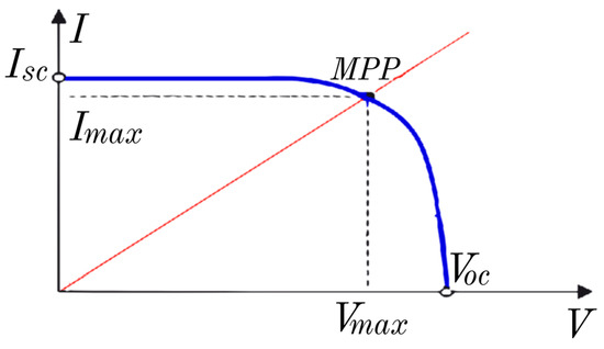
Figure 2.
The characteristic solar cell I-V.
As depicted in Figure 2, to trace the curve comprehensively, a variable load is needed to identify all potential operating points along it. It is important to recognize that multiple I-V curves can be derived from a single panel by varying conditions such as temperature and irradiance. The point of maximum power occurs where the curve shows the highest combination of current and voltage the panel can provide. These are the critical values targeted by the MPPT (Maximum Power Point Tracking) algorithm [18,19].
2.1. Modeling and Characteristics
For the purposes of emulation, the model of one diode from the photovoltaic solar cell will be taken as a reference, as shown in Figure 3. In this circuit, it can be observed that a photovoltaic solar cell works as a controlled source, where the control variable is the irradiance or solar radiation.
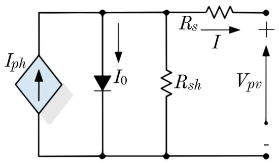
Figure 3.
Solar cell diode model [20].
The basic diode equation for a photovoltaic solar cell is (1).
where
I represents the total circuit current;
Iph is the photocurrent generated by illumination;
I0 denotes the dark saturation current of the diode;
V stands for the voltage across the diode;
q is the charge of an electron (1.602 × 10⁻¹⁹ C);
k is the Stefan–Boltzmann constant (1.381 × 10⁻²³ J/K);
T is the temperature in Kelvin.
The equation incorporating solar irradiance and internal resistances within a photovoltaic (PV) cell model, aiming to represent the dynamics of the cell comprehensively, involves parameters like Iph(G) for the photo-generated current, I0 for the dark saturation current, V for the voltage across the cell, I for the output current, Rs for the series resistance, Rsh for the parallel (shunt) resistance, and factors for temperature and irradiance effects. This model accounts for the non-ideal behavior of real PV cells by including resistances that affect the panel’s efficiency and performance. The Iph(G) increases with solar irradiance (G, in W/m2).
The mathematical function representing Iph as a function of solar irradiance (G) typically assumes direct proportionality between the irradiance and the current generated by the cell. A simplified form could be Iph = k⋅G, where k is a proportionality constant depending on the specific characteristics of the photovoltaic cell, including its efficiency and area. This model reflects how the photo-generated current increases linearly with irradiance under the assumption that all other factors remain constant.
A more detailed form of Iph considers various factors, including the panel’s efficiency dependency on temperature and specific material parameters. However, due to complexity and variability among different solar panel technologies, there is not a universally accepted ‘non-simplified form’ that does not consider specific panel model parameters. For precise details, consulting a solar panel’s technical datasheet is necessary, where equations based on its characteristics and response to irradiance and temperature are provided.
A detailed and widely accepted expression for Iph, considering both irradiance (G) and temperature (T), could be the following:
where Iph,STC is the photocurrent under standard test conditions (normally, 1000 W/m2 irradiance and 25 °C temperature), GSTC is the standard test condition irradiance (1000 W/m2), G is the current irradiance, TSTC is the standard test condition temperature (25 °C), T is the current module temperature, and α is the temperature coefficient of the current, indicating how the current varies with temperature. This formula reflects how the current generated by the cell increases with irradiance and adjusts with changes in module temperature. Reference [20] can be studied for a deeper analysis of the equations describing the operation of photovoltaic solar panels.
Let us discuss the emulated panel’s characteristics. The panel is a YINGLI 60 CELL-series, 40 mm, model YL250p-29b. The YL250p-29b photovoltaic panel has 60 cells connected in series, with an open-circuit voltage of 38.40 Vdc. According to its datasheet, under standard test conditions (STCs), it possesses the following electrical characteristics: The maximum rated power is 250 W, and the efficiency panel is 15.3%. At full power, its voltage is 30.4 V, and its current is 8.24 A. The open circuit voltage is 38.4 V, while the short circuit current is 8.79 A.
Beyond the I-V solar panel characteristics, the emulator also needs to consider various technical parameters: the temperature coefficient of the current α = 0.00385; the reference inverse saturation current (Io), which in this case is 1.2723 × 10⁻¹⁰ A; the electron charge q = 1.602 × 10⁻¹⁹ C; the diode’s ideality factor n = 0.9985; the Stefan–Boltzmann constant (K = 1.3806 × 10⁻²³ J/K); the energy bandgap at the reference temperature (EgRef = 1.212 J); and the values of the resistances Rsh = 364.52 Ω and Rs = 0.42475 Ω.
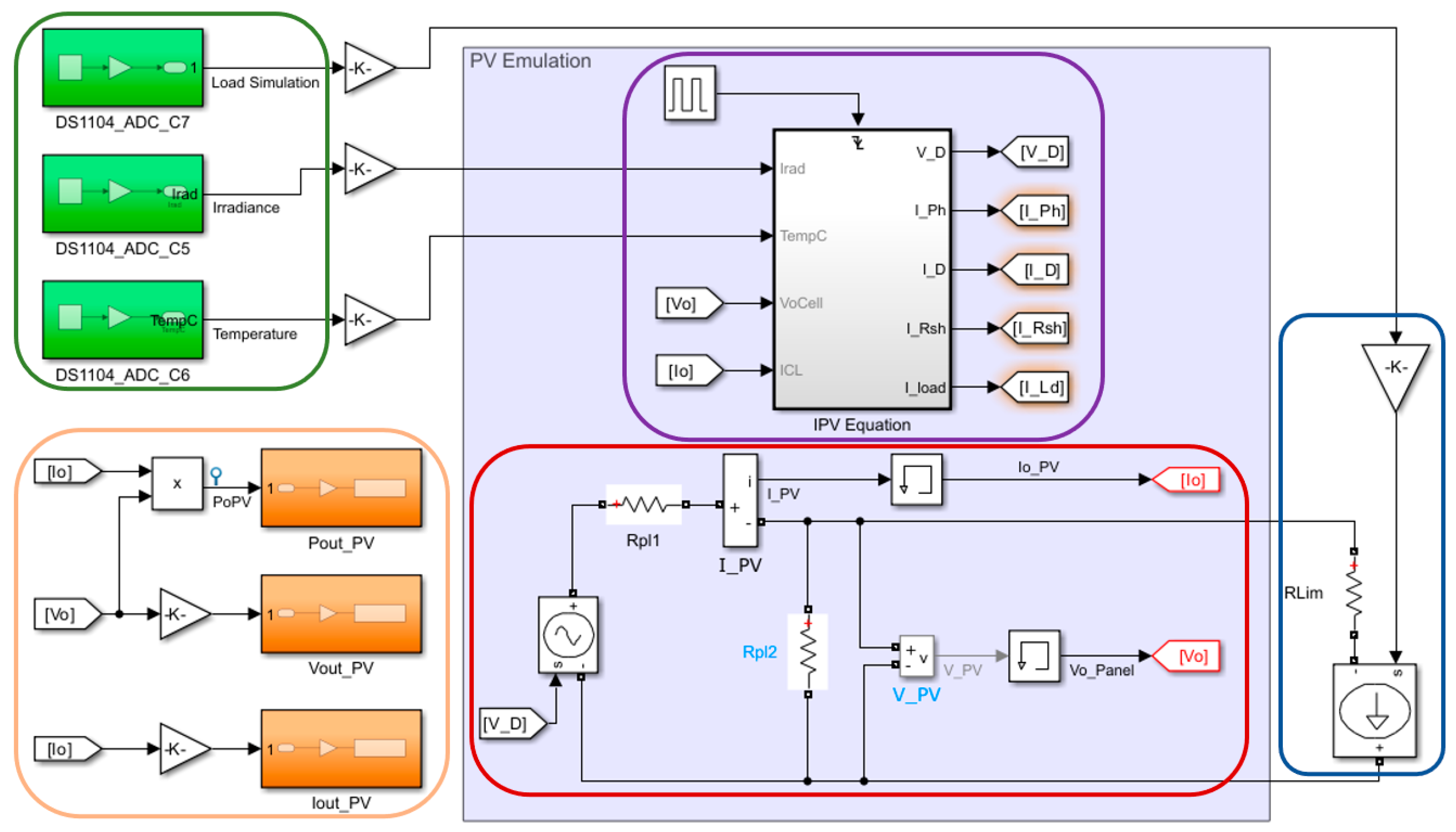
Figure 4 showcases the SIMULINK model representing the solar panel. As can be observed in the figure, two subsystems are implemented to determine the essential variables for solar panel voltage control according to weather and load conditions. The part marked in purple is a MATLAB script for the implementation of Equations (1) and (2). This script receives two variables, the panel temperature and the irradiance; the inputs to the model are highlighted in green. Since it is an emulation, the values for the mentioned signals are acquired through a data acquisition system that allows for the emulation of the PV array. The system marked in red is an electrical circuit similar to the single-diode model of the solar panel, the difference being that in the circuit there is no current source that depends on irradiance. Instead, the voltage across the panel terminals is used for its implementation, with ‘V_D’ being equal to the variable ‘V’ in Equation (1). The controlled current source, the gain, and the ‘RLim’ resistance aim to recreate the current demand in the PV. When a current demand is simulated through the dependent current source, the voltage V_D drops, as shown in Figure 1. The value of the voltage V_D is determined using Equation (1), where the current I (I_PV in Figure 4) is the current delivered by the PV panel to the load emulated by the circuit marked in blue. The simulation of the current demand is also performed by one of the analog inputs of the data acquisition system, which is described in a subsequent section. The model’s inputs and outputs are highlighted in green and orange, respectively. With these inputs and outputs, changes in the variables of voltages, currents, and powers in a PV system are obtained.
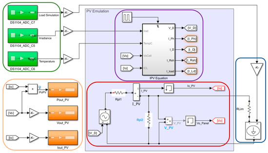
Figure 4.
Solar panel model for emulation.
2.2. PV Simulation
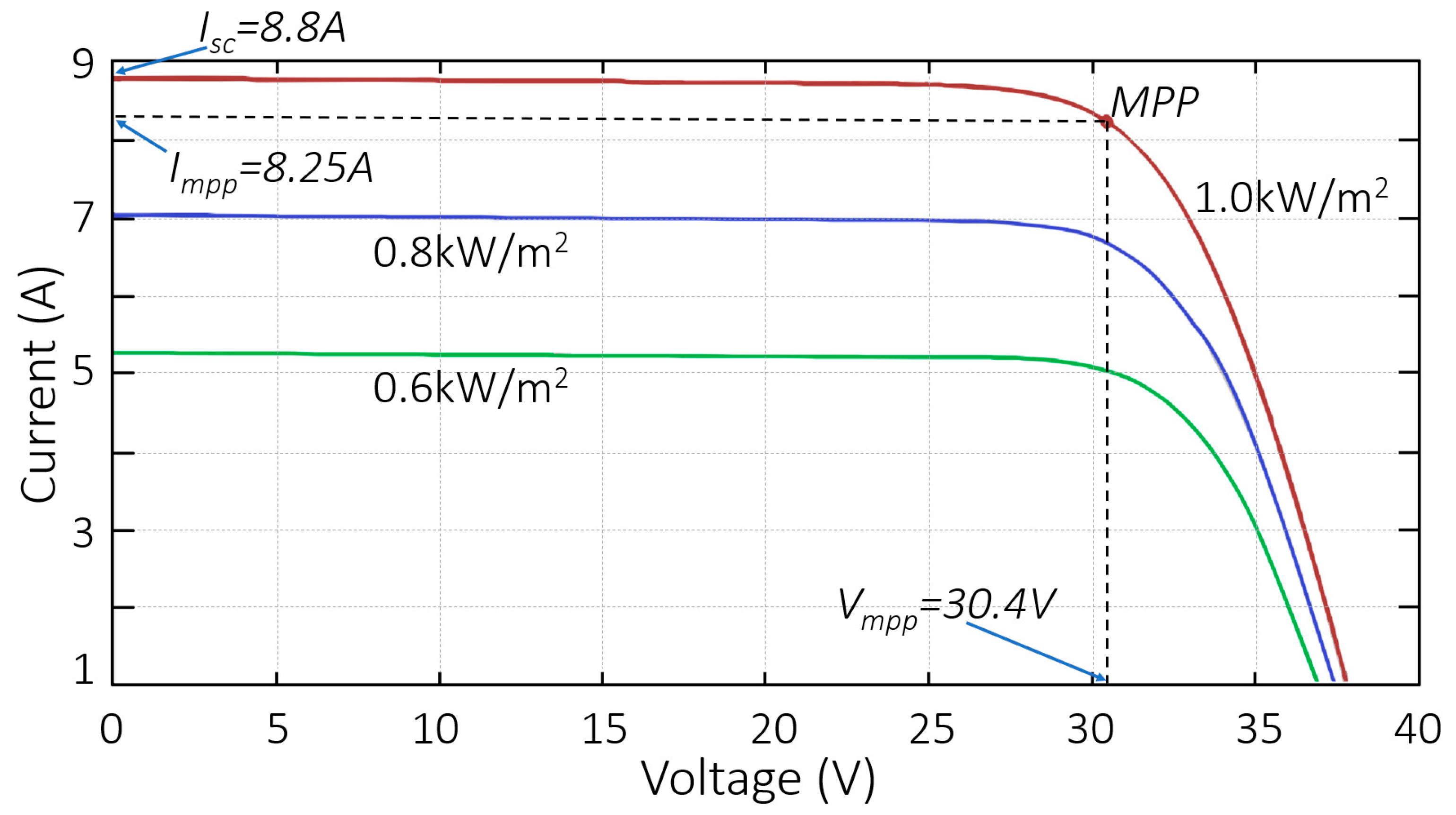
To obtain the array I-V graph of the emulated panel array, it was necessary to create a script that simulated the current demand (I) from 0 A up to its short-circuit value. This behavior is achieved by manipulating the controlled current source shown in Figure 4. The manipulation of this source is performed using a DC voltage, which is injected through one of the analog inputs of the data acquisition card. Figure 5 demonstrates how this emulator automatically transitions from one curve to another, replicating the panel’s array behavior, which is subjected to temperature and solar radiation. This ensures that the emulator maintains characteristics consistent with the referenced model.
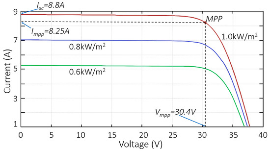
Figure 5.
I-V characteristic curve of the solar panel.
Taking as a reference the panel’s response curve at a power of 1 kW/m2, we find that the values for current and voltage at the maximum power point differ slightly from those reported by the manufacturer, as do the open-circuit operating conditions. The comparison of these values can be seen in Table 1, where the error percentage is also recorded. The error percentage is attributed to calculating the diode current in the panel model.

Table 1.
Panel parameters and simulation results.
To represent the solar panel’s module, a programable voltage source was devised to accept a reference signal from the dSPACE control board, which receives the signal from the simulation. This setup will regulate the voltage specified by the model using a linear regulator. Additionally, sensors will provide feedback on voltage and the current of the voltage source to ensure correct operation.
A complete scheme of the emulator power supply is shown in Figure 6. The core objective was to enable voltage regulation through a control signal, leading to the selection of an LM317, which allows for voltage adjustment by varying the input current at the ADJUST pin. It is important to remember that the reference signal for the voltage comes from the dSPACE board; an isolating barrier featuring isolation amplifiers was incorporated for protection. To augment the output current capacity of the regulator, the inclusion of a pass transistor was necessary, ensuring stable system regulation. Furthermore, to supply adequate power to the system, three additional regulators were implemented, as indicated by the blue boxes. The green boxes represent a control stage designed to distribute the current across each regulator evenly.

Figure 6.
Schematic diagram of the panel’s array emulator.
3. Multiplier SEPIC Converter
Power electronics is an essential discipline in the efficient conversion and control of electrical energy [21,22,23]. Its applications range from renewable energy generation systems to everyday consumer electronic devices. In the context of solar energy, power electronics play a crucial role in enabling the conversion of the energy captured by solar panels into usable and regulated forms of electrical power. The field of the DC-DC converter has many applications in PV panels [23,24,25]. The SEPIC (Single-Ended Primary Inductor Converter) is a power converter topology that offers advantages in terms of flexibility and efficiency, making it particularly suitable for solar panel emulators, where irradiance and environmental conditions can vary widely. Implementing a solar panel emulator based on a SEPIC converter allows for the recreation of the electrical characteristics of a real solar panel, facilitating the design and testing of photovoltaic systems under controlled and repeatable conditions.
With the aim of obtaining power from the PV-emulated circuit, a Multiplier SEPIC Converter was implemented. This converter will allow it to carry out the maximum power from the PV emulator using a traditional MPPT algorithm like Perturb and Observe (P&O). The strategy is to increase the voltage provided by the PV array with the SEPIC converter. At the same time, the SEPIC converter output voltage is supplied to a resistor, and the SEPIC voltage is changed to find the emulated PV array’s maximum power point (MPP).
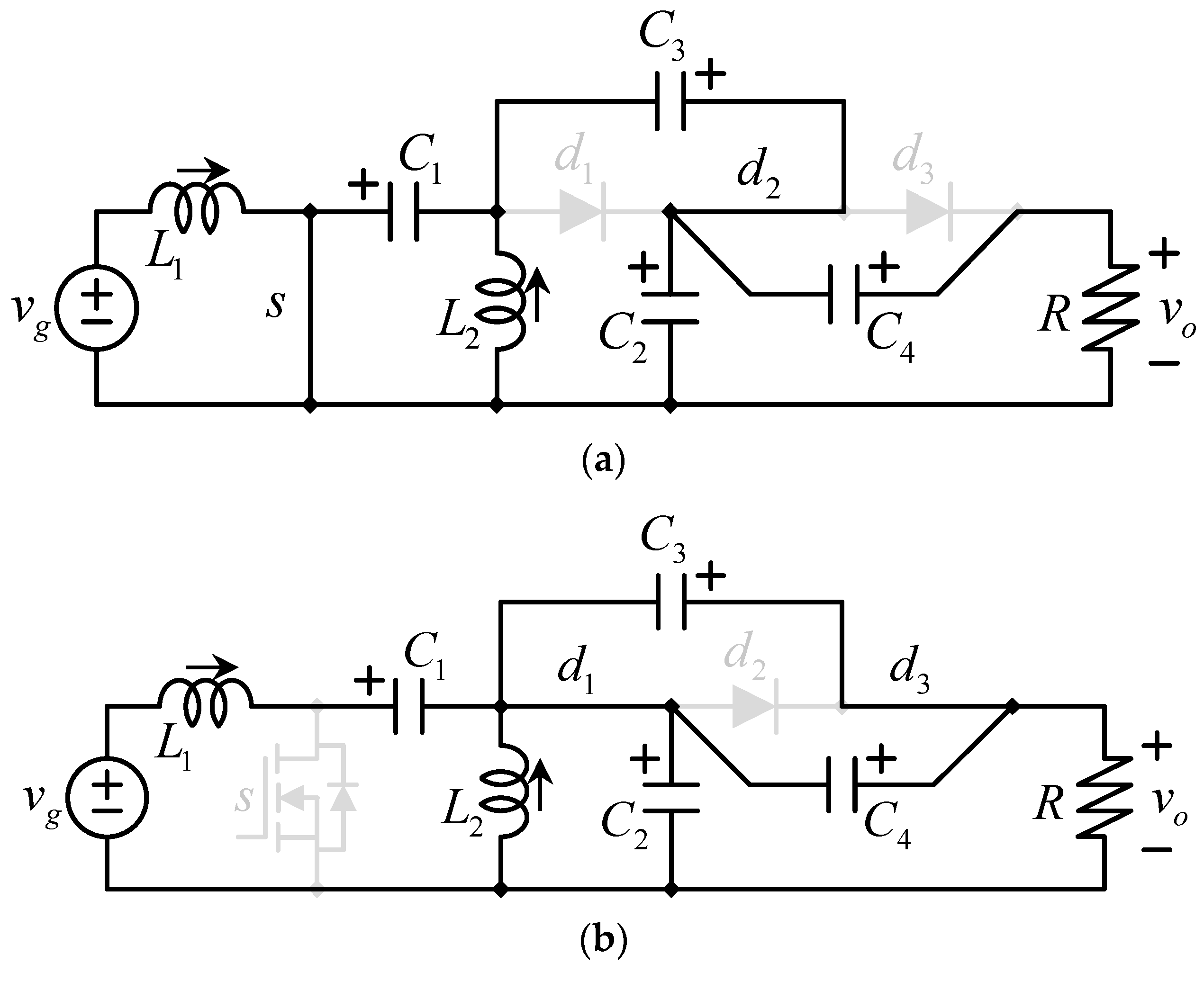
The Single-Ended Primary-Inductor Converter (SEPIC) is composed of a switch (s) (which can be synthesized with a transistor), a diode (d1), inductors (L1 and L2), and capacitors (C1 and C2); the load can be represented as a resistor (R), as shown in Figure 7a. The SEPIC is capable of providing output voltages that are higher and lower than the input voltage.
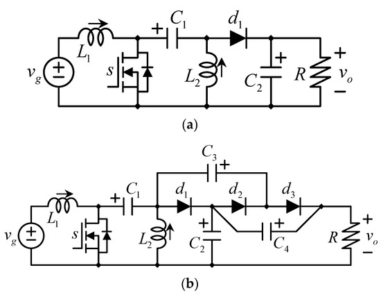
Figure 7.
(a) SEPIC converter. (b) Multiplier SEPIC converter.
An improved version of the conventional SEPIC [26,27] includes a hybrid topology with diode-capacitor multipliers, known as the Dickson charge pump. Figure 7b illustrates a SEPIC that incorporates a 2x multiplier.
The transistor closes and opens periodically with a constant switching frequency (fSW); the inverse of the switching frequency is called the switching period (TSW). During a switching period, the transistor remains closed for a duration called ton, and subsequently, it remains closed for a time called toff. Evidently, the relation between the switching period and the times in which the transistor is closed and open can be expressed as in (3):
A duty cycle or duty ratio (D) and its complement can be defined as in (4) and (5).
Figure 8 shows the equivalent circuits according to the switch state (open or closed). The fundamental operation of the SEPIC, as depicted in Figure 7a, can be explained with the following steps and by observing the equivalent circuits in Figure 8.
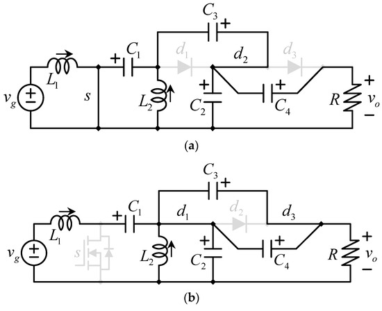
Figure 8.
Switching states when (a) the transistor is on and (b) when the transistor is off.
- (i)
- (ii)
- When the switch opens (see Figure 8b), it allows L1’s current to infuse C1 with a positive voltage (in alignment with the designated signs) since they are connected in series, and the current gets through the positive voltage sign of C1.
- (iii)
- The switching action of the transistor is periodic; it inevitably closes again, but this time the capacitor C1 already has some charge; it gets in parallel connection with the inductor L2, facilitating C1 in endowing L2 with a positive flow of current.
- (iv)
- Upon the transistor’s subsequent opening, L2’s current moves through d1, enriching C2 with a positive charge.
This sequence of actions detailing the operation of the traditional SEPIC illustrated in Figure 7a is equally applicable to the configuration shown in Figure 7b, with the following additional steps:
- (v)
- With the transistor open and L2’s current passing through d1, as seen in Figure 8b, the negative terminals of C3 and C4 are conjoined at the same potential, subsequently allowing C3 to engage d3 to positively charge C4.
- (vi)
- With the transistor’s closure, C1 aligns in a series setup with C2, as shown in Figure 8a, which then permits the charging of C3 through the engagement of d2.
The circuit in Figure 7b operates a diode-capacitor voltage multiplier, specifically a 2x multiplier in this scenario, which can be expanded through the addition of more diodes and capacitors. Calculating the average voltage across L1 over a single switching cycle while employing the conventional small ripple approximation [23] results in (6).
where vL1ton represents the voltage across L1 with the switch closed and vL1toff denotes the voltage across L1 when the transistor is open. This formula can be expressed in relation to the duty ratio outlined in (2) as follows.
The voltage across L1 during each equivalent circuit or switching state can be derived from the circuits depicted in Figure 8.
At equilibrium, the average voltage across the inductors equals zero, resulting in a steady current. Following Equation (7) and incorporating Equations (8) and (9), this can be articulated as (10).
Similarly, the (average) voltage across L2 can be expressed as (11).
And the voltage in each state can also be determined by applying the KVL in Figure 8 as in (12) and (13).
In the equilibrium condition or steady state, the voltage in L2 must also be in that state, which can be written using (11) to (13) as (14).
From (10), the voltage in C2 can be expressed as (15).
Substituting (15) in (11) leads to the following:
Finally, the load voltage is given by the series connection of C2 and C4, which can be expressed as (19).
The voltage gain is significant. Figure 9 illustrates the voltage gain relative to the duty cycle or duty ratio expressed in (19).
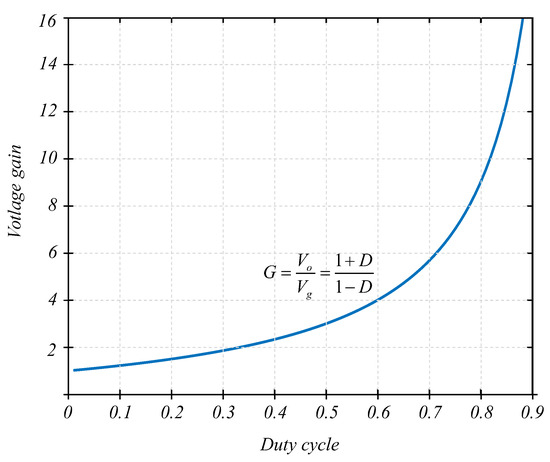
Figure 9.
Voltage boost factor vs. duty cycle or duty ratio.
As can be seen in Figure 8b, the voltage that the transistor needs to block (when it is open) is relatively low in comparison to the output voltage. This attribute is advantageous, as it allows for the use of transistors rated for lower voltages in the construction of high-voltage converters, embodying the essence of multilevel converters. Contrary to this, in other configurations like the cascaded boost converter, the final transistor must withstand the entire output voltage. This requirement caps the maximum achievable output voltage to the voltage rating of the transistor. Moreover, transistors designed to handle higher voltages typically exhibit greater on-resistance than those intended for lower voltages.
A further benefit of the Multilevel SEPIC lies in the ability to enhance the voltage gain without augmenting the count of inductors. Inductors are bulky, costly, and challenging to encapsulate. Moreover, a singular transistor suffices irrespective of the level count, as adding more transistors necessitates additional circuitry.
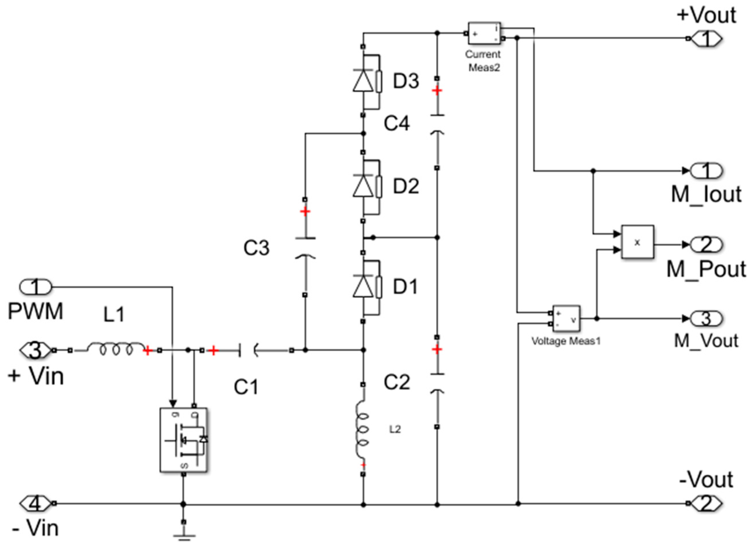
Figure 10 displays the simulated model of the proposed Multiplier SEPIC in MatlabSimulink R2023b software; the values of the Multiplier SEPIC components and the selected semiconductors are detailed in Table 2.
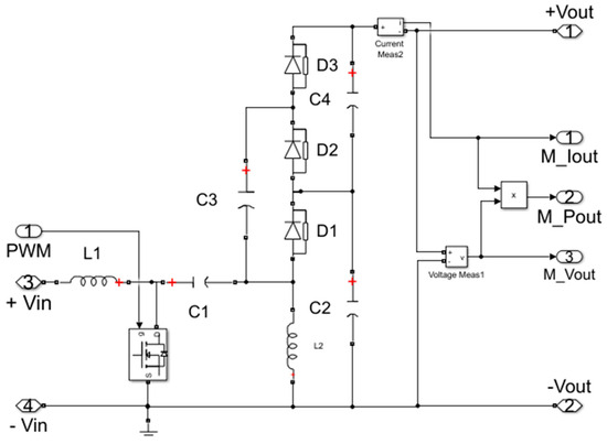
Figure 10.
Schematic of the Multiplier SEPIC.
Table 2.
Selected components of the Multiplier SEPIC.
Multiplier SEPIC Simulation and Hardware Test
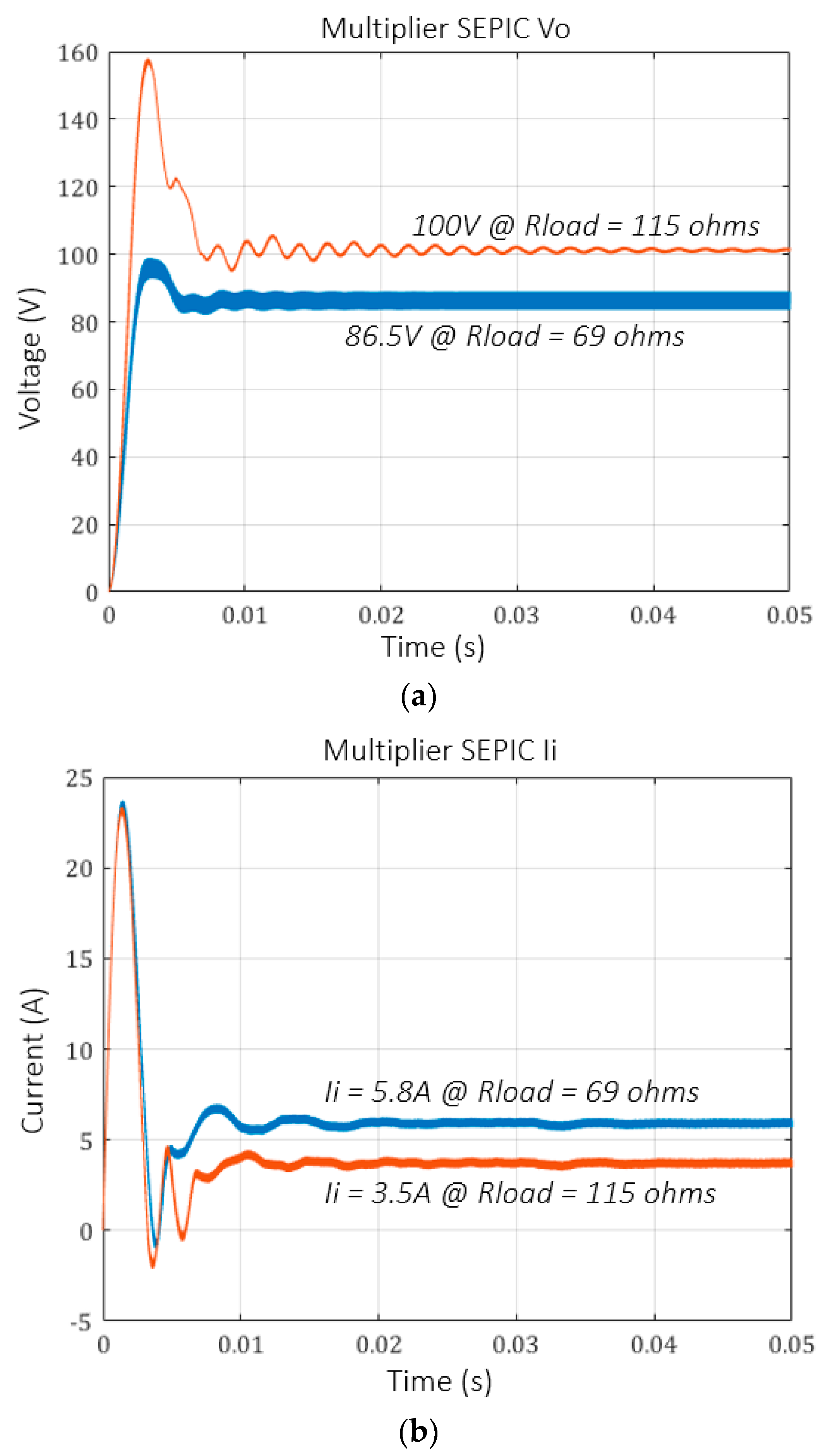
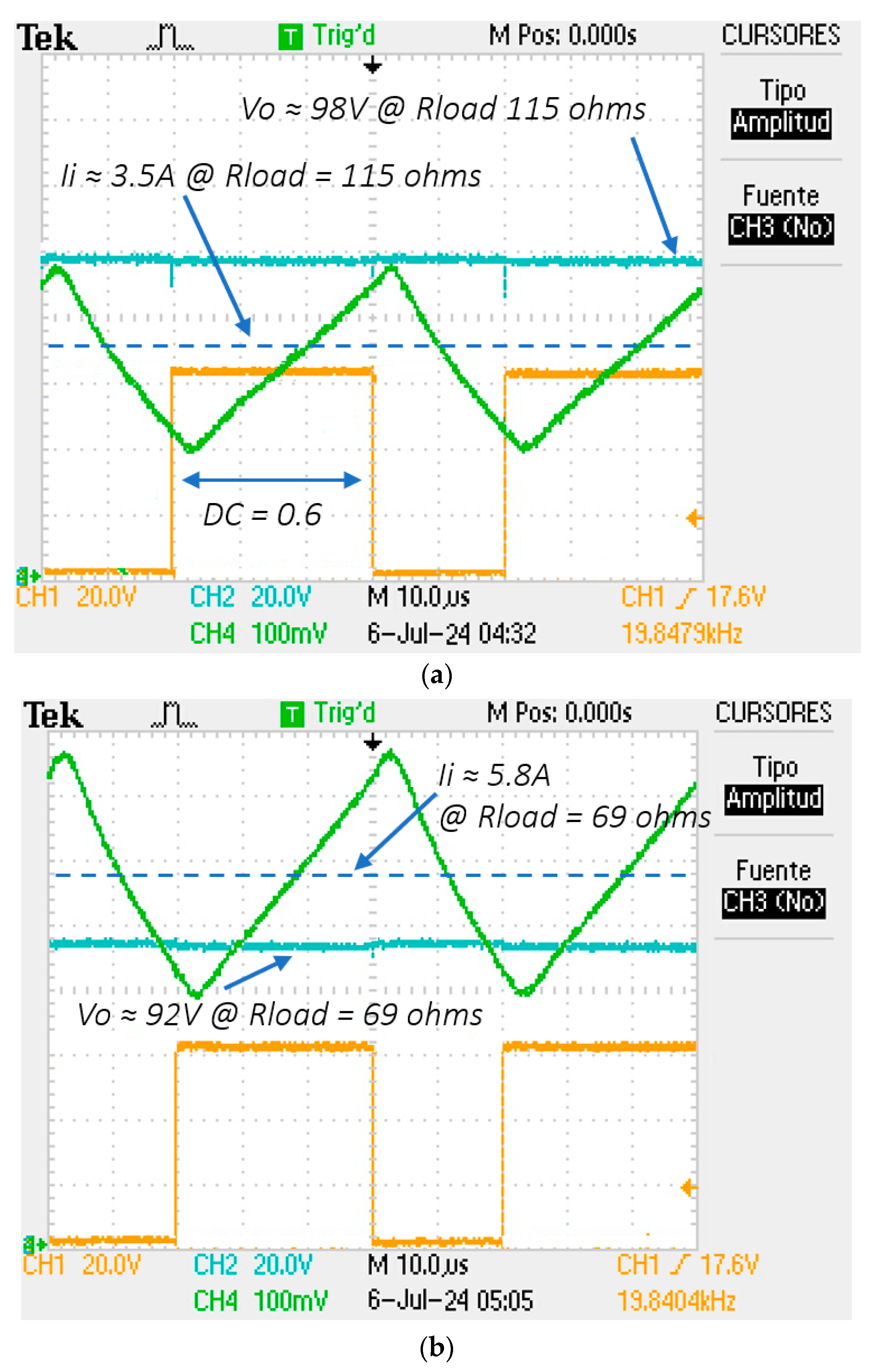
For the simulation and testing of the Multiplier SEPIC, an input voltage of 25 V, a useful cycle of 60%, and two different load resistances of 115 and 69 Ω were established in open loop. For the first case, with a load equal to 115 Ω, the output voltage should be 100 V, a theoretical current of approximately 0.88 A should be delivered, and the input current to the Multiplier SEPIC will be 3.5 A on average. For the second case, with a load equal to 69 ohms, the output voltage should be 100 V, a theoretical current of approximately 1.45 A should be delivered, and the input current to the Multiplier SEPIC will be 5.8 A on average.
Figure 11a shows the output voltages for the two cases, while Figure 11b shows the output and input currents. The hardware results for the Multiplier SEPIC are shown in Figure 12a,b. The over peaks and transients observed in the simulations are due to numerical approximations and initial conditions, which are not present in the real hardware. In boot cases, simulations, and hardware implementation, the output voltage was reduced by approximately 4 V. The current was measured with a sensing probe, with a 1 A/0.1 V reduction rate.
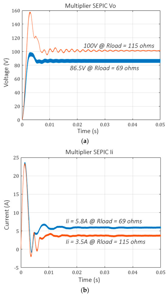
Figure 11.
(a) Simulation results for Vo. (b) Simulation results for Ii.
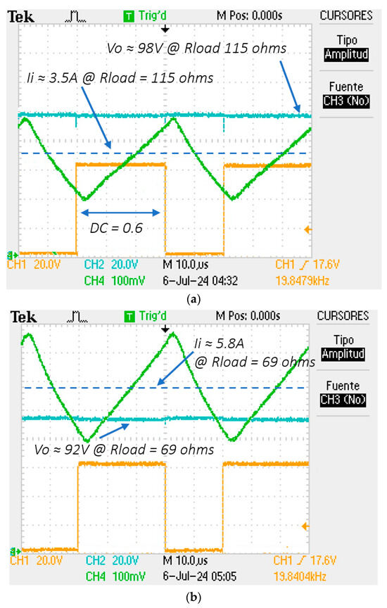
Figure 12.
(a) Experimental results for the case with Rload = 115 ohms load. (b) Experimental results for the case with Rload = 69 ohms load.
4. Simulation Results for the PV + Multiplier SEPIC
Table 3 outlines the specifications of the panel array used in the simulation; they correspond to a temperature equal to 25 °C and an irradiance of 1000 W/m2.
Table 3.
Input and output converter parameters.
Utilizing this information, one can refer to the I-V curve presented in Figure 5 to establish the necessary current and voltage values for designing the converter. The converter is designed to have an output power of 250 W and will operate in the linear region with a maximum duty ratio of 45% to ensure operation within a safe range. From this, the load resistance can be determined, which in turn allows for the calculation of the converter’s output voltage and current.
After defining the input and output variables, the next step is to choose the components to be used. It is crucial to select an adequate transistor; in this case, a metal–oxide–semiconductor field-effect transistor (MOSFET) was chosen to minimize energy losses through heat dissipation.
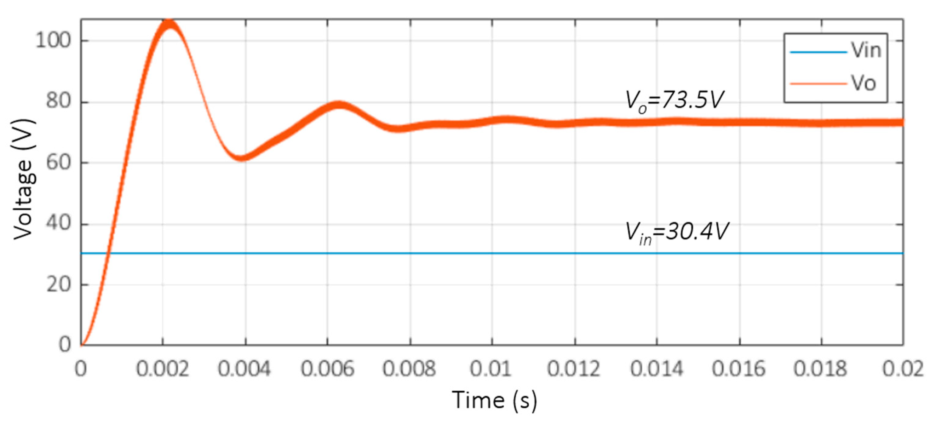
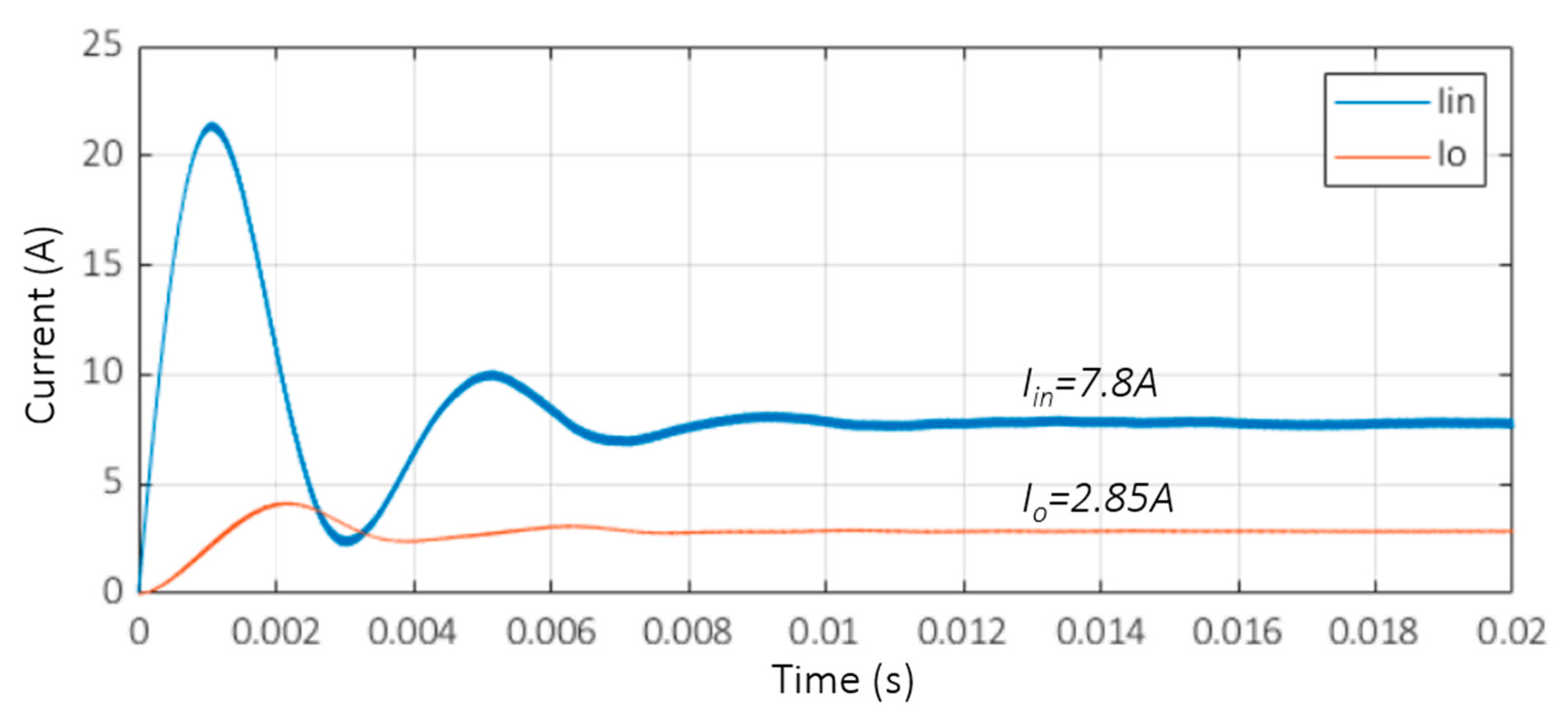
The results of the simulation described above are shown, with Figure 13 revealing that the voltage achieved was very near the ideal 80.25 V value, with minimal losses of 6.75 V. Additionally, the voltage gain achieved was 2.42, whereas, theoretically, with a 45% duty ratio, the ideal value is three, indicating that the system’s efficiency in terms of voltage gain is 91.6%. Furthermore, Figure 14 shows the current converter and illustrates that the emulator is not ideal and incurs power losses. When the output power is 209.5 W, the input power is about 237.1 W, resulting in an efficiency of 88.4%. The overpeaks and transients in Figure 13 and Figure 14 are due to numerical approximations and initial conditions, which are not present in the real hardware.

Figure 13.
Input (red) and output (blue) converter voltage signals.
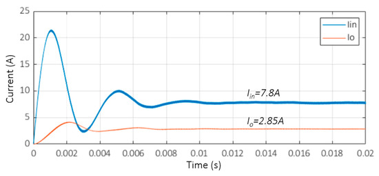
Figure 14.
Input (red) and output (blue) converter currents.
The block diagram shown in Figure 15 corresponds to the complete system. The system was run with 0.286 uS of the sample period in the simulation, adhering to the Nyquist criterion. This adjustment was necessary because the SEPIC operated with a sample period of 28.5714 µS (35 KHz) and it is the fastest subsystem. For example, the panel’s array emulator had a sample period of 1 mS and the Maximum Power Point Tracker (MPPT) algorithm ran with a sample period of 28 mS. Other parameters were the load resistance of 25.8 Ω over the total period simulation, which had a duration of 9 s.
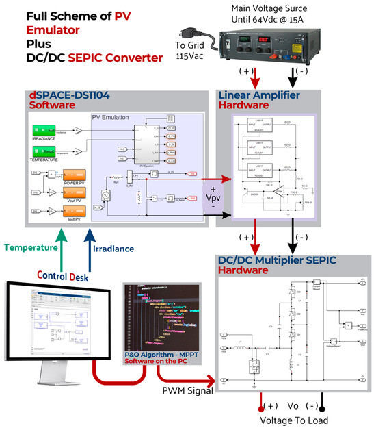
Figure 15.
System simulation.
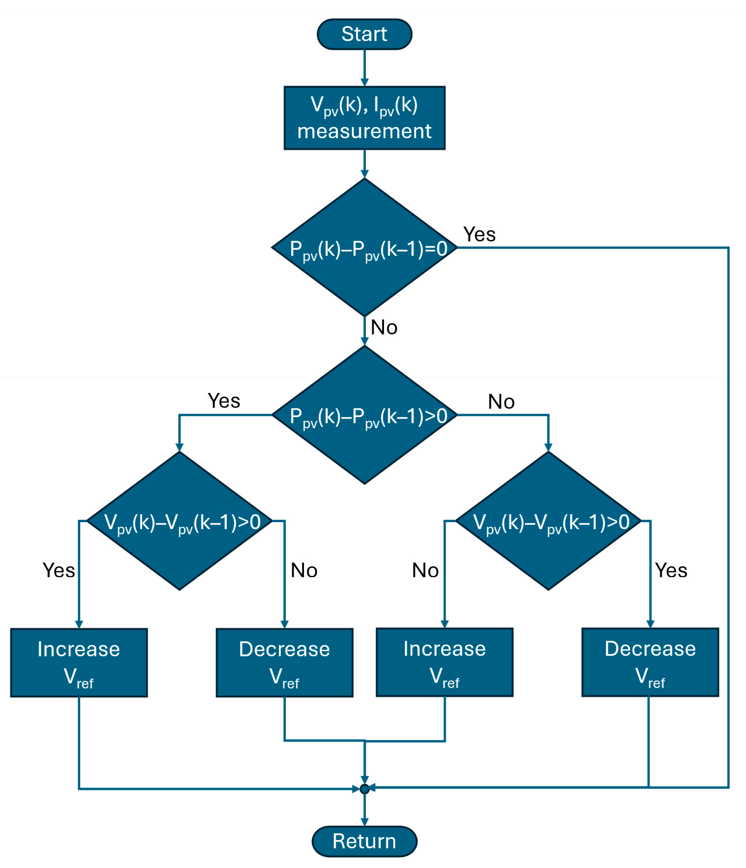
Among the various Maximum Power Point Tracking (MPPT) techniques, the Perturb and Observe (P&O) technique is the most widely used, being extensively implemented in commercial photovoltaic inverters due to the use of low-cost microcontrollers. However, despite its simplicity and reliability, the P&O algorithm has some major disadvantages. First, when the tracking reaches the vicinity of the MPP, the operating point tends to oscillate around it, resulting in a persistent fluctuation in the output power and, consequently, reducing the system quality. Secondly, P&O is prone to losing the search direction, meaning that it fails to adapt to changes in irradiance, causing the operating point to deviate from the MPP curve. This deviation also results in energy loss. In the work presented, the traditional Perturb and Observe technique was implemented to test the PHIL system rather than as an algorithm that excels in efficiency and effectiveness for finding and following the MPP. The P&O technique operates with a DC/DC or DC/AC converter, which helps extract power from the photovoltaic panel. When the panel’s output power changes, the voltage across its output terminals, Vpv, also changes. The algorithm periodically increases or decreases the output voltage of the photovoltaic module to estimate a power value. Subsequently, the power obtained in the current cycle, P(k), is compared with the power from the previous cycle, P(k − 1). If a perturbation is introduced in the system voltage, this will cause an increase or decrease in the output power. If the perturbation in the voltage causes an increase in power, the next perturbation is applied in the same direction as initially applied.
Conversely, if the power decreases, the next perturbation is applied in the opposite direction. After several perturbations, the algorithm converges to the maximum power point (MPP). Once the maximum power is reached, if the power in the next instant decreases, the perturbation should be applied in the opposite direction. Figure 16 shows the P&O algorithm. The emulation platform allows other algorithms to be used in the emulation process. Testing the platform with algorithms other than P&O was not within the scope of this article; rather, the aim was to demonstrate a platform development that will allow for their easy subsequent implementation.
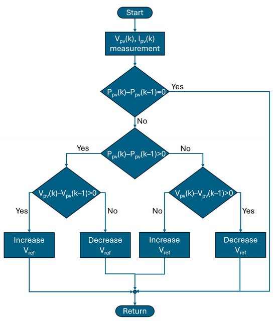
Figure 16.
P&O algorithm.
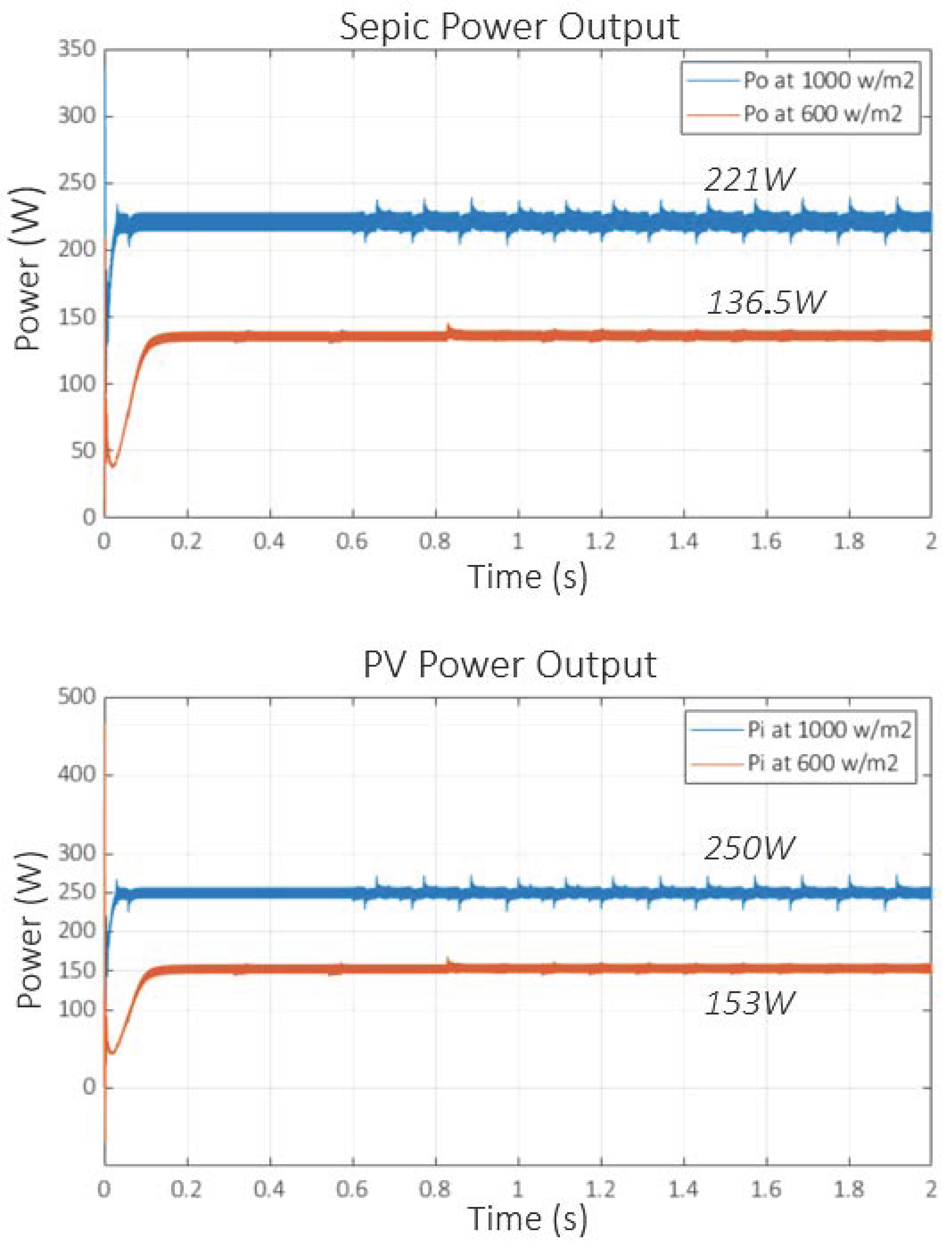
To test the MPPT algorithm and the Multilevel SEPIC regulator working together, a simulation was first conducted with two scenarios of constant solar radiation: the first with continuous radiation of 1000 W/m2, and the second with continual radiation of 600 W/m2—both scenarios with a panel temperature of 25 °C.
The results of this simulation are presented in Figure 17, Figure 18 and Figure 19. In Figure 17, the input power represents the maximum provided by the solar module. However, the output power demonstrates that the ripple caused by the MOSFET switching and the duty cycle adjustments enacted by the MPPT algorithm resulted in the system operating at an efficiency level below 100%. Figure 17 shows the power at the MPP. The peaks and transients in power are due to the typical oscillation around the MPP of the P&O algorithm; these variations can be reduced by adjusting the reference voltage increment of the P&O algorithm. Notably, under real environmental conditions, an increase in solar radiation or changes due to shadows are gradual, so the power transitions will be smoother.
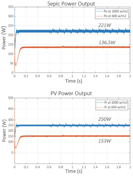
Figure 17.
System power with the SEPIC running in the dynamic mode.
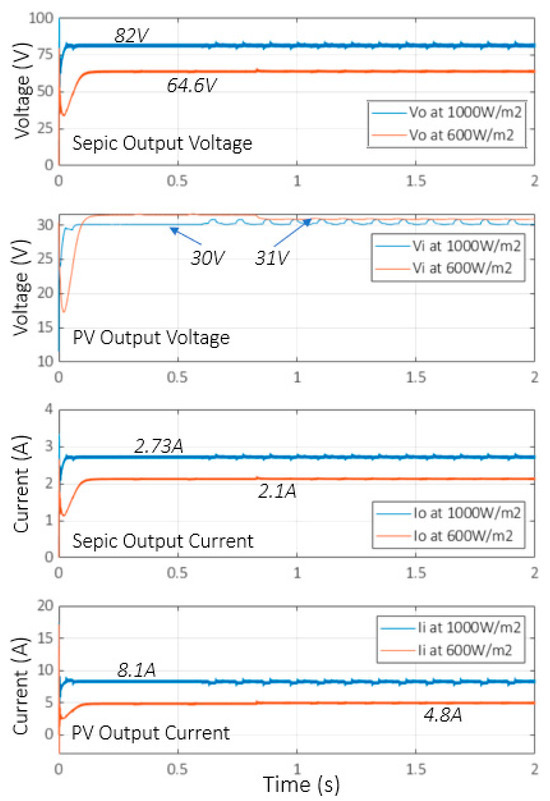
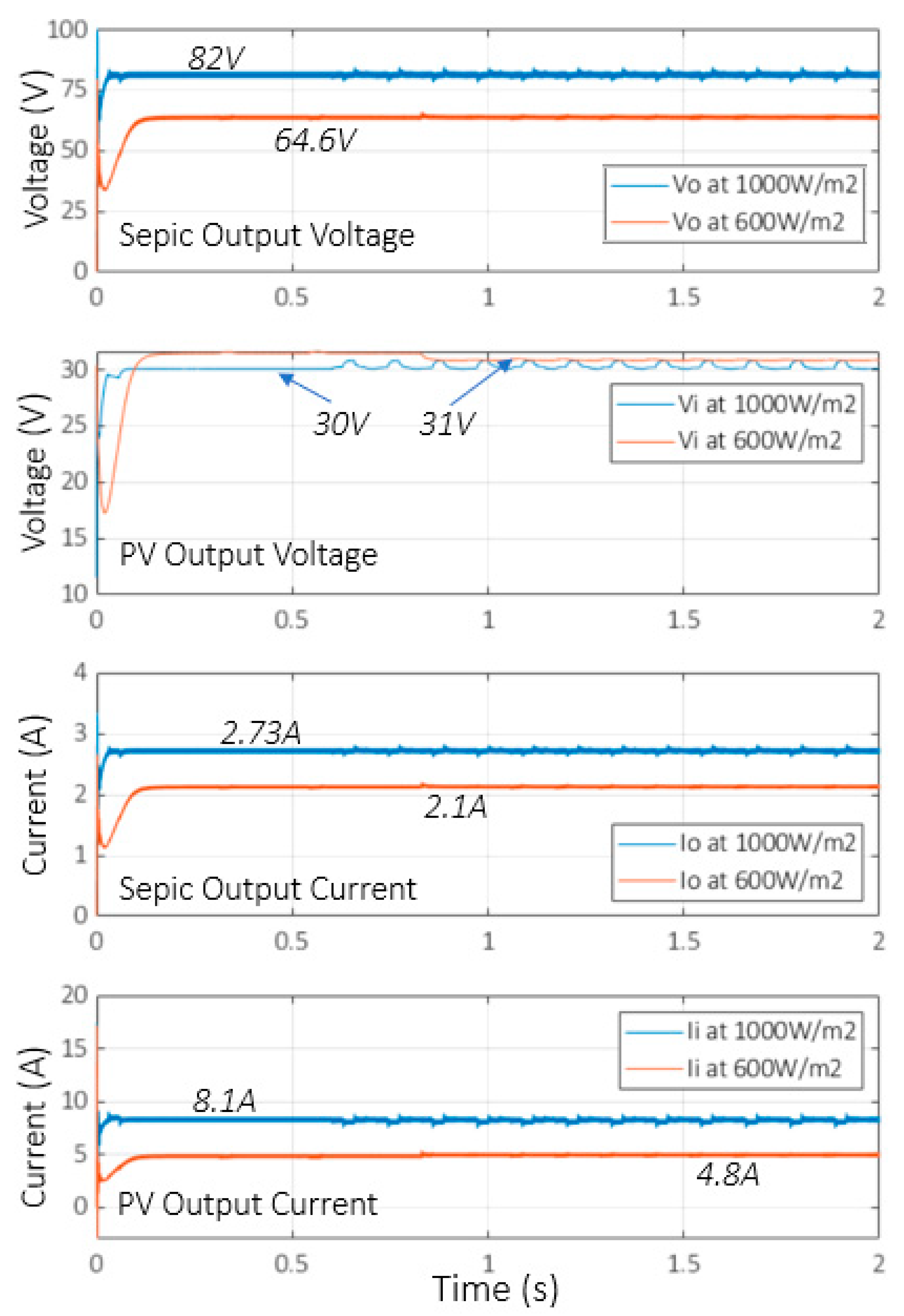
Figure 18.
Voltage and current signals with the dynamic mode for the SEPIC.
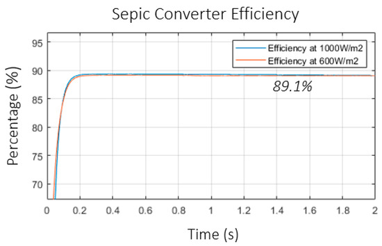
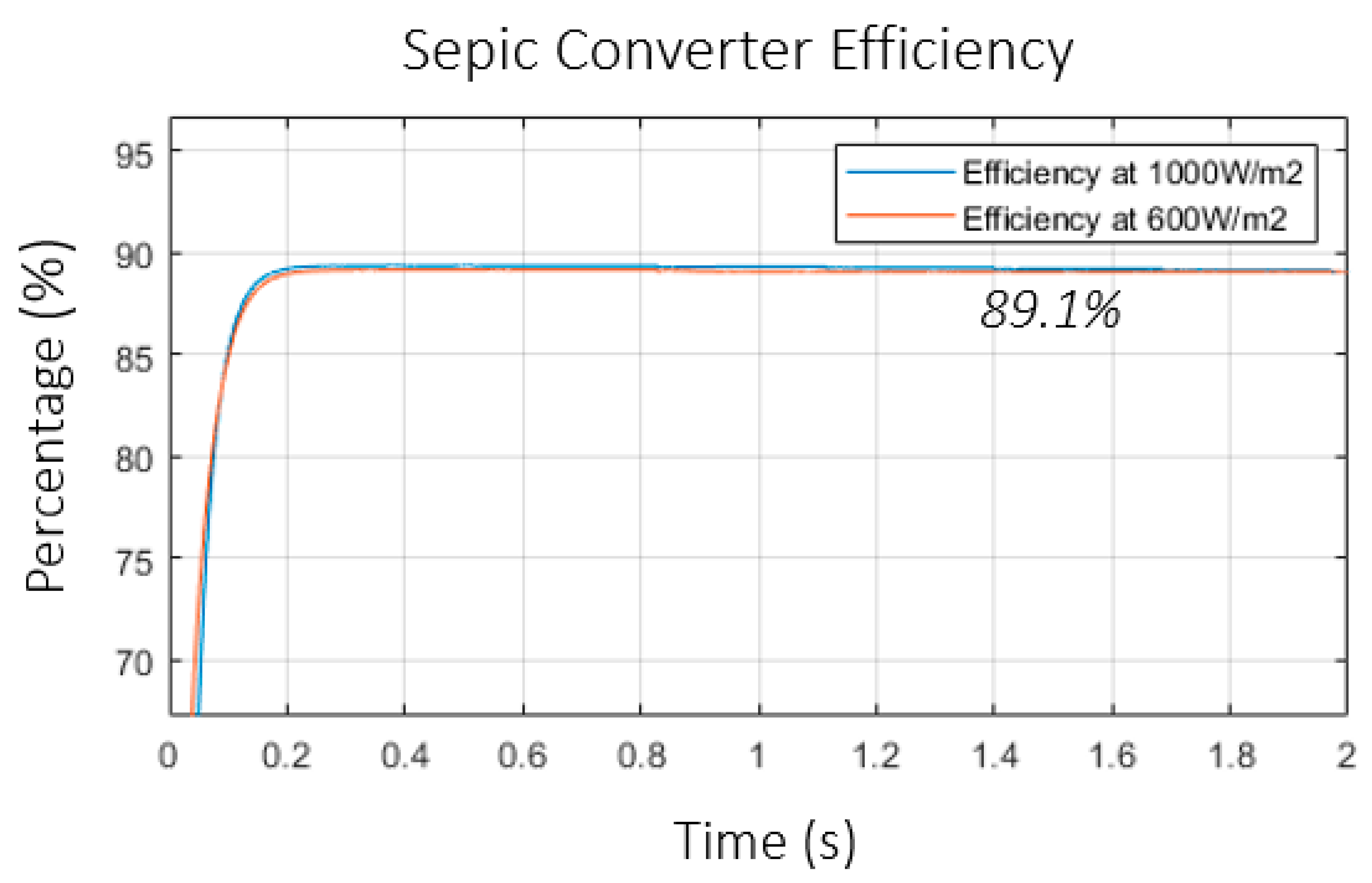
Figure 19.
System efficiency during the dynamic mode of the SEPIC.
Figure 18 shows the voltage evolution at the output of the Panel, Vpv, and at the output of the Multilevel SEPIC converter, Vo. The voltage and current variations can be observed as the result of changes in the reference voltage of the P&O algorithm.
Finally, Figure 19 shows the evolution of the system’s efficiency under the two operating conditions. Since the initial conditions of the Multilevel SEPIC converter components were set to zero at the start of the simulation, oscillations occurred in the behavior of all the measured variables, which decreased once normal operating conditions were reached.
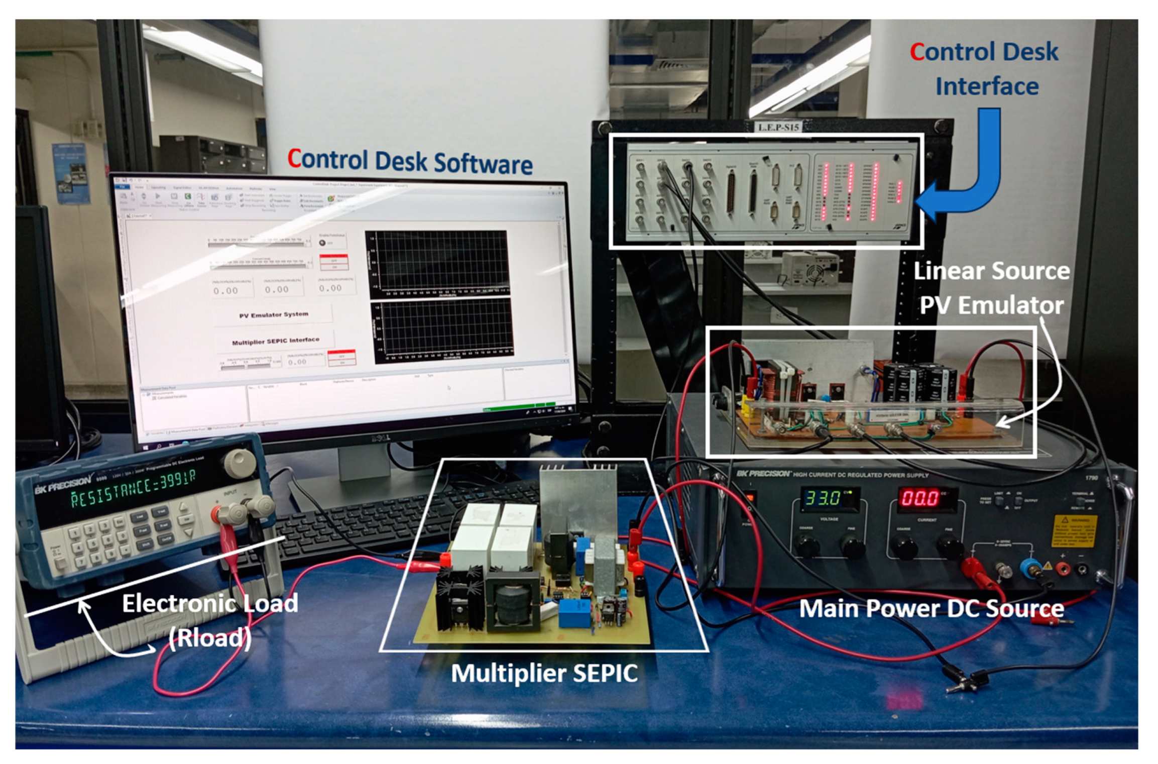
5. Hardware Results
Figure 20 shows the hardware implementation of the PHIL system. The figure highlights the interface in the control desk, the connection panel of the DS1104 data acquisition card, the linear source that emulates the behavior of the PV, the SEPIC Multiplier, and the electronic load in charge of emulating the system’s power demand. The electronic load fulfills the load resistance functions in the implementation.

Figure 20.
Hardware implementation of PV Emulator + Multiplier SEPIC.
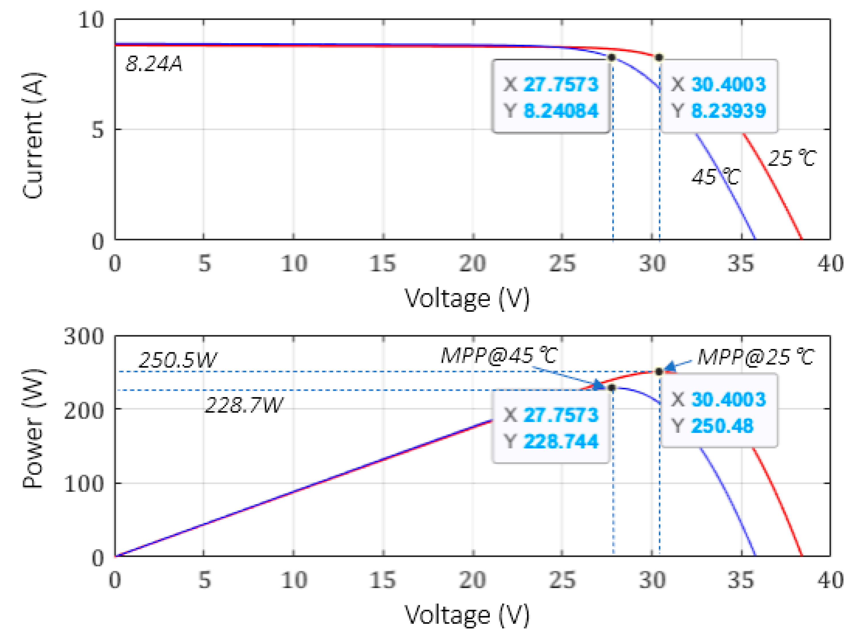
In a photovoltaic solar panel, temperature directly impacts the power the panel can deliver, as evidenced by analyzing Equation (2), where the photocurrent shows a direct dependence on temperature. In a PV curve like the one in Figure 21, the influence of temperature on the MPP can be observed, which decreases in value as the temperature increases, directly affecting the panel’s voltage. In Figure 21, the red line shows the PV curve for a temperature of 25 °C @ 1000 W/m2 radiation, while the blue line shows the same curve for a temperature of 45 °C. The effect of temperature was considered for the Testbed used for the hardware validation of the designed prototype.
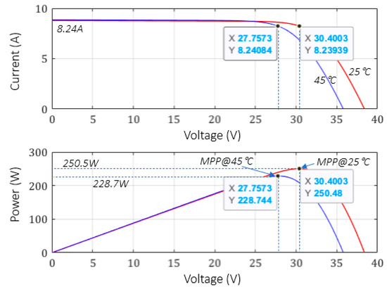
Figure 21.
Modification of the MPP due to temperature change. The red curves are at 25 °C, and the blue curves are at 45 °C.
The DS1104 software 6.5 develops the Testbed for the laboratory prototype. At t = 0 s, a step in solar radiation of 600 W/m2 and a temperature of 25 °C are generated, at which point the MPPT algorithm begins the search for the MPP. It takes approximately 6 s for the MPPT algorithm to reach the MPP. Ten seconds later, t = 10 s, a change in the panel temperature is generated, shifting from 25 °C to 45 °C. With this change, a decrease in the power provided by the panel should be observed, as shown in Figure 21.
Afterward, at t = 14.5 s, the solar radiation reference change is generated at 1000 W/m2 and a temperature of 45 °C. Once again, after this change in solar radiation, an increase in the power provided by the solar panel is expected. Finally, at t = 25 s, the temperature reference changes from 45 °C to 25 °C, which would be expected to increase the panel’s power due to the temperature decrease. On a normal day, the behavior of solar radiation does not experience sudden changes, so transients are not large. Furthermore, the MPPT algorithm can be executed with a much longer sampling time. In this scenario, the efficiency of the Multiplier SEPIC was around 88%, similar to the simulation results. It should be noted that the MPPT algorithm is executed every 200 mS, which is sufficient time for the Multiplier SEPIC converter to stabilize after a change in the duty cycle reference.
To calculate the power of the emulated panel, measurements of panel voltage and panel current are acquired via DS1104, which are measured at the output of the linear source using Hall Effect current sensors AMPLOC 25, LEM50, and LV25P voltage sensors. The PWM signal that activates the MOSFET of the Multiplier SEPIC also comes from the DS1104 system, where the MPPT algorithm is located. Once the measurement is performed, the data are transferred to Matlab for further processing and visualization.
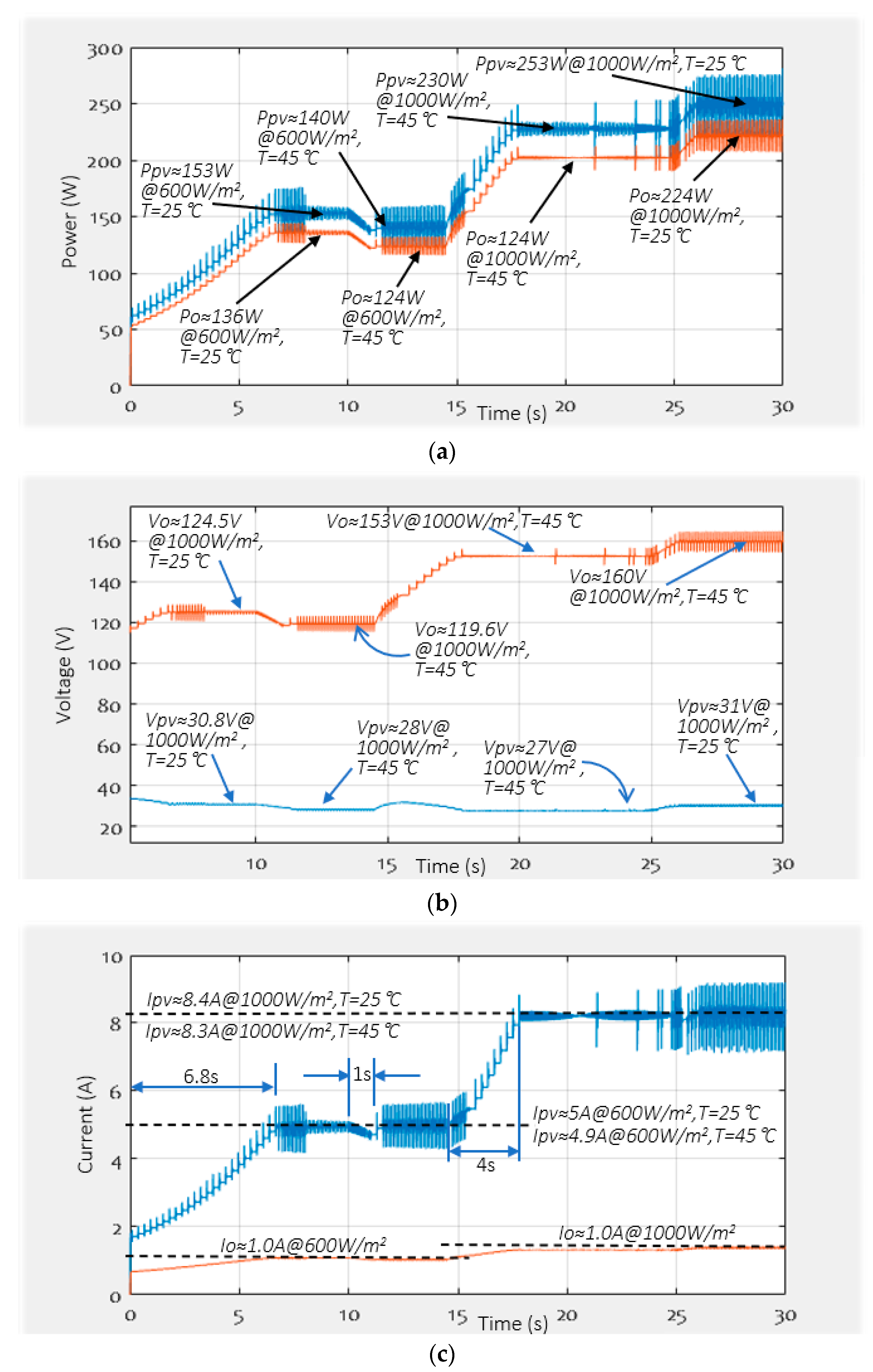
Figure 22a shows the evolution of the power output from the panel, Ppv, and the power output from the Multilevel SEPIC, Po. As expected, the power provided by the photovoltaic panel decreases when the temperature reference changes at t = 10 s, consistent with the expected behavior observed in Figure 21. Additionally, when the solar radiation reference changes from 600 W/m2 to 1000 W/m2, there is also an increase in the panel’s power, as anticipated. Finally, the panel’s power increases when the panel temperature drops to 25 °C. Comparing the panel’s output voltages, current, and power in the emulated system for radiation of 1000 W/m2, they are very similar to those expected from the panel according to the manufacturer’s parameters shown in Figure 21.

Figure 22.
(a) Power evolution of Ppv panel (blue) and Po in the output of Multiplier SEPIC (red). (b) Voltage evolution of Vpv panel (blue) and Vo in the output of Multiplier SEPIC (red). (c) Current evolution of Ipv panel (blue) and Io in the output of Multiplier SEPIC (red).
Figure 22b,c show the evolution of the voltage and current in the laboratory hardware using an Rload of 115 Ω. As expected for a panel, the output voltage decreases when the temperature increases, causing the panel’s power to change. When the temperature and irradiance change, the panel voltage also changes by around 30 V, as can be seen in Figure 22b, as expected, and, similarly, the output voltage of the Multilevel SEPIC changes when the algorithm searches for the MPP. Figure 22c shows the current evolution in the panel, whose short-circuit limit is constrained by the irradiance. Equations (1) and (2) illustrate this dependence, which can be graphically observed in Figure 5.
Figure 22c also shows the times at which the MPP is reached: between 1 s and 2 s, when temperature changes occur, and between 3 s and 6 s, when abrupt changes in irradiance occur.
6. Conclusions
This study uses a novel approach to model, design, and emulate a solar array feeding a DC-DC SEPIC multiplier converter with a Maximum Power Point Tracker (MPPT). The approach uses a Power Hardware-In-the-Loop (PHIL) DSpace platform for experimental validation along with a real DC-DC SEPIC multiplier converter. The article’s contributions can be summarized as follows: (i) The application of an innovative emulation technique in a didactic PV + Multiplier SEPIC system: Our approach uniquely combines PHIL emulation with a real DC-DC converter, providing a versatile tool for emulating solar panel arrays under various conditions. This allows the simulation of renewable energy sources, offering a high degree of precision and flexibility in the emulation of different scenarios, the implementation of different MPPT algorithms, and experimentation with other types of DC/DC and DC/AC converters. (ii) The experiments conducted using the DSpace platform demonstrated the effectiveness and the reliability of our PHIL emulator in replicating the behavior of solar arrays connected to a DC-DC converter, including variations in sunlight intensity and other environmental factors, such that it can serve as a teaching and laboratory tool for experimentation at low cost. (iii) The successful development and validation of our PHIL emulator provides a powerful tool for researchers and engineers in the field of renewable energy. By allowing for detailed and accurate simulation of solar power systems, our work facilitates the exploration of new control strategies, the optimization of energy conversion processes, and the enhancement of system efficiency and stability.
Finally, our research contributes to the broader goal of advancing sustainable energy technologies. By improving our ability to simulate and study solar power systems, we are better equipped to develop innovative solutions that will increase the viability and efficiency of renewable energy, paving the way for a more sustainable and environmentally friendly future. New control algorithms can be tested with the proposed equipment in future work.
Author Contributions
J.P.C. contributed to the conceptualization of the article, J.C.R.-C. contributed to the methodology, J.P.C. contributed to the software, J.C.R.-C. contributed to the formal analysis, J.P.C. and J.C.R.-C. wrote the draft and contributed to the manuscript preparation. All authors have read and agreed to the published version of the manuscript.
Funding
The authors would like to thank the Universidad Panamericana and the Universidad Autonoma de Occidente.
Data Availability Statement
Data are contained within the article.
Acknowledgments
The authors would like to thank the Universidad Autónoma de Occidente in Colombia and the Universidad Panamericana in Mexico.
Conflicts of Interest
The authors declare no conflicts of interest.
References
- Subbulakshmy, R.; Palanisamy, R.; Alshahrani, S.; Saleel, C.A. Implementation of Non-Isolated High Gain Interleaved DC-DC Converter for Fuel Cell Electric Vehicle Using ANN-Based MPPT Controller. Sustainability 2024, 16, 1335. [Google Scholar] [CrossRef]
- Khan, M.R.; Haider, Z.M.; Malik, F.H.; Almasoudi, F.M.; Alatawi, K.S.S.; Bhutta, M.S. A Comprehensive Review of Microgrid Energy Management Strategies Considering Electric Vehicles, Energy Storage Systems, and AI Techniques. Processes 2024, 12, 270. [Google Scholar] [CrossRef]
- Daccò, E.; Falabretti, D.; Ilea, V.; Merlo, M.; Nebuloni, R.; Spiller, M. Decentralised Voltage Regulation through Optimal Reactive Power Flow in Distribution Networks with Dispersed Generation. Electricity 2024, 5, 134–153. [Google Scholar] [CrossRef]
- Bordbari, M.J.; Nasiri, F. Networked Microgrids: A Review on Configuration, Operation, and Control Strategies. Energies 2024, 17, 715. [Google Scholar] [CrossRef]
- Min, C.; Kim, H. A Practical Framework for Developing Net-Zero Electricity Mix Scenarios: A Case Study of South Korea. Energies 2024, 17, 926. [Google Scholar] [CrossRef]
- Gayathri, R.; Chang, J.-Y.; Tsai, C.-C.; Hsu, T.-W. Wave Energy Conversion through Oscillating Water Columns: A Review. J. Mar. Sci. Eng. 2024, 12, 342. [Google Scholar] [CrossRef]
- Mihalič, F.; Truntič, M.; Hren, A. Hardware-in-the-Loop Simulations: A Historical Overview of Engineering Challenges. Electronics 2022, 11, 2462. [Google Scholar] [CrossRef]
- Yousefzadeh, M.; Hedayati Kia, S.; Hoseintabar Marzebali, M.; Arab Khaburi, D.; Razik, H. Power-Hardware-in-the-Loop for Stator Windings Asymmetry Fault Analysis in Direct-Drive PMSG-Based Wind Turbines. Energies 2022, 15, 6896. [Google Scholar] [CrossRef]
- Hermassi, M.; Krim, S.; Kraiem, Y.; Hajjaji, M.A.; Alshammari, B.M.; Alsaif, H.; Alshammari, A.S.; Guesmi, T. Design of Vector Control Strategies Based on Fuzzy Gain Scheduling PID Controllers for a Grid-Connected Wind Energy Conversion System: Hardware FPGA-in-the-Loop Verification. Electronics 2023, 12, 1419. [Google Scholar] [CrossRef]
- Dini, P.; Saponara, S. Modeling and Control Simulation of Power Converters in Automotive Applications. Appl. Sci. 2024, 14, 1227. [Google Scholar] [CrossRef]
- Lamo, P.; de Castro, A.; Sanchez, A.; Ruiz, G.A.; Azcondo, F.J.; Pigazo, A. Hardware-in-the-Loop and Digital Control Techniques Applied to Single-Phase PFC Converters. Electronics 2021, 10, 1563. [Google Scholar] [CrossRef]
- Estrada, L.; Vázquez, N.; Vaquero, J.; de Castro, Á.; Arau, J. Real-Time Hardware in the Loop Simulation Methodology for Power Converters Using LabVIEW FPGA. Energies 2020, 13, 373. [Google Scholar] [CrossRef]
- Sanchez, A.; Todorovich, E.; De Castro, A. Exploring the Limits of Floating-Point Resolution for Hardware-In-the-Loop Implemented with FPGAs. Electronics 2018, 7, 219. [Google Scholar] [CrossRef]
- De Souza, I.D.T.; Silva, S.N.; Teles, R.M.; Fernandes, M.A.C. Platform for Real-Time Simulation of Dynamic Systems and Hardware-in-the-Loop for Control Algorithms. Sensors 2014, 14, 19176–19199. [Google Scholar] [CrossRef] [PubMed]
- Regatron Programmable Power Supplies. Available online: https://www.regatron.com/programmable-power-supplies/en/#hardware-in-the-loop (accessed on 16 June 2024).
- Chroma Solar Array Simulator Model 62000H-S Series. Available online: https://www.chromaate.com/en/product/solar_array_simulator_62000h_s_series_205 (accessed on 16 June 2024).
- Martínez, J.R.; Rengifo, H.R.; Córdoba, J.S.; Palacios, J.; Posada, J. Design and Implementation of a Multiplier SEPIC Converter to Emulate a Photovoltaic System Using Power HIL. In Proceedings of the 2019 FISE-IEEE/CIGRE Conference—Living the energy Transition (FISE/CIGRE), Medellin, Colombia, 4–6 December 2019; pp. 1–7. [Google Scholar]
- Olayiwola, T.N.; Hyun, S.-H.; Choi, S.-J. Photovoltaic Modeling: A Comprehensive Analysis of the I–V Characteristic Curve. Sustainability 2024, 16, 432. [Google Scholar] [CrossRef]
- Pan, W.; Zhang, Y.; Jin, W.; Liang, Z.; Wang, M.; Li, Q. Photovoltaic-Based Residential Direct-Current Microgrid and Its Comprehensive Performance Evaluation. Appl. Sci. 2023, 13, 12890. [Google Scholar] [CrossRef]
- Duffie, J.A.; Beckman, W.A. Solar Engineering of Thermal Processes, Photovoltaics and Wind; Wiley: New York, NY, USA, 1991; pp. 762–772. [Google Scholar]
- Rashid, M.H. Power Electronics: Circuits, Devices, and Applications, 3rd ed.; Pearson Education: Hoboken, NJ, USA, 2009; pp. 289–292. [Google Scholar]
- Mohan, N.; Undeland, T.M.; Robbins, W.P. Power Electronics in Converters, Applications, and Design, 3rd ed.; Whiley: Hoboken, NJ, USA, 2002. [Google Scholar]
- Erickson, R.W.; Maksimovic, D. Fundamentals of Power Electronics, 3rd ed.; Springer: New York, NY, USA, 2020. [Google Scholar]
- Valdez-Resendiz, J.E.; Mayo-Maldonado, J.C.; Alejo-Reyes, A.; Rosas-Caro, J.C. Double-Dual DC-DC Conversion: A Survey of Contributions, Generalization, and Systematic Generation of New Topologies. IEEE Access 2023, 11, 38913–38928. [Google Scholar] [CrossRef]
- Rosas-Caro, J.C.; Mayo-Maldonado, J.C.; Valdez-Resendiz, J.E.; Alejo-Reyes, A.; Beltran-Carbajal, F.; López-Santos, O. An Overview of Non-Isolated Hybrid Switched-Capacitor Step-Up DC–DC Converters. Appl. Sci. 2022, 12, 8554. [Google Scholar] [CrossRef]
- Rosas-Caro, J.C.; Mayo-Maldonado, J.C.; Valdez-Resendiz, J.E.; Salas-Cabrera, R.; Gonzalez-Rodriguez, A.; Salas-Cabrera, E.N.; Cisneros-Villegas, H.; Gonzalez-Hernandez, J.G. Multiplier SEPIC converter. In Proceedings of the CONIELECOMP 2011, 21st International Conference on Electrical Communications and Computers, Cholula, Puebla, Mexico, 28 February–2 March 2011; pp. 232–238. [Google Scholar]
- Rosas-Caro, J.C.; Sanchez, V.M.; Vazquez-Bautista, R.F.; Morales-Mendoza, L.J.; Mayo-Maldonado, J.C.; Garcia-Vite, P.M.; Barbosa, R. A novel DC-DC multilevel SEPIC converter for PEMFC systems. Int. J. Hydrogren Energy 2016, 41, 23401–23408. [Google Scholar] [CrossRef]


Disclaimer/Publisher’s Note: The statements, opinions and data contained in all publications are solely those of the individual author(s) and contributor(s) and not of MDPI and/or the editor(s). MDPI and/or the editor(s) disclaim responsibility for any injury to people or property resulting from any ideas, methods, instructions or products referred to in the content. |
© 2024 by the authors. Licensee MDPI, Basel, Switzerland. This article is an open access article distributed under the terms and conditions of the Creative Commons Attribution (CC BY) license (https://creativecommons.org/licenses/by/4.0/).