Abstract
The electrical properties of solution-processed spinel nickel cobaltite (NiCo2O4) nanoparticulated-based metal oxide hole transporting layers are investigated using conductivity and Hall effect measurements. The mechanism of electrical conductivity of NiCo2O4-based electronic films as a function of temperature indicates hopping-type carrier transport. We show that NiCo2O4 hole transporting layers (HTLs) have suitable conductivity, low toxicity, and relatively low processing temperature, parameters that are important for electronic materials specifications of high performance and environmentally friendly emerging photovoltaics. As a proof of concept, NiCo2O4 and Cu-SCN surface-modified NiCo2O4 are incorporated as HTLs for non-fullerene acceptor Organic Photovoltaics (OPVs), and the photovoltaic performance results of the corresponding OPVs are presented.
1. Introduction
To make the transition to low-carbon energy systems, research on solar energy technology that attempts to transform sunlight directly into electrical energy is essential [1]. Investigations to improve the efficiency and stability of emerging photovoltaic technologies have been accelerated by the rapid advances of innovative electronic materials in the field of material science.
Organic photovoltaics (OPVs) are one of the most promising emerging solar cell technologies due to their benefits regarding low solution processing manufacturing for large-scale roll-to-roll production and less impact on the environment after disposal in comparison to other photovoltaics technologies [2,3,4,5,6,7,8]. Recently, non-fullerene acceptors (NFAs) within the active layers of solution-processed organic photovoltaics (OPVs)have greatly improved their power conversion efficiency (PCE) in the range of 19% [9,10].
Hole-transporting layers (HTLs) and electron transport layers (ETLs) are essential interlayers in OPVs since they increase the collecting capabilities of hole and electron charges toward the anode and cathode electrodes, respectively, and, therefore, increase the power conversion efficiency (PCE) of OPVs [11,12]. However, the development of appropriate charge-selective contacts between the active layer and the electrodes in OPVs presents challenges [13,14].
For the normal OPV device architecture, the most used conducting polymer HTL is the Poly(3,4-ethylenedioxythiophene)-poly(styrene sulfonate) (PEDOT:PSS) due to its low cost, limited toxicity, easy solution processing, and high work function (WF). However, due to its hygroscopic and acidic properties, PEDOT:PSS creates stability issues during solar cell operation under environmental conditions, which leads to the usage of p-type metal oxides as HTLs in OPVs instead, which in some cases provide improved lifetime performance due to their chemical and moisture resistance [7,15].
The most common p-type metal oxides that have been employed as HTLs in OPVs are MoO3, NiO, WO3, Fe3O4, and CuOx [16,17,18,19,20]. Nevertheless, despite their aforementioned advantages, they suffer from low electrical conductivity, which can limit the performance of the respective solar cell devices. Furthermore, high vacuum techniques for deposition, as well as temperatures above 400 °C in order to achieve enhanced metal oxide crystallinity, are usually required for their synthesis, resulting in increased device manufacturing costs and simultaneously restricting their application to flexible photovoltaic applications [21,22].
Nickel cobaltite (NiCo2O4) is an environmentally friendly p-type transparent conductive oxide (TCO) material with the following characteristics: a wide optical band gap (~2.4 eV), a deep-lying valence band (~5.3 eV) and a conductivity of two orders of magnitude greater than NiO and Co3O4. Due to those reasons, nickel cobaltite is considered a reliable metal-oxide electronic material for use in optoelectronics [23].
We have previously reported the solution combustion-synthesized (SCS) of a smooth, compact, and functional electronic film of the highly conductive spinel nickel cobaltite (NiCo2O4) nanoparticles utilizing tartaric acid as a fuel to produce monodispersed particles with mean size of ~4 nm, which was successfully introduced as hole transporting layers in inverted perovskite solar cells (PVSCs) [24].
In this paper, we examine the implementation of neat and Cu-SCN surface-modified nickel cobaltite (NiCo2O4) as a hole transporting layer (HTL) on the performance of non-fullerene acceptor (PBDB-TF-T1 (T1): ITIC-4F) based OPVs that have been processed using the low-toxicity solvent O-xylene. Furthermore, we study the electrical characteristics of NiCo2O4 HTLs using D.C. conductivity measurements in the temperature range of 100 to 340 K. The above measurements allow us to identify “hopping-like” charge transport as the conductivity mechanism and calculate the “hopping” distance of the solution-processed nanoparticulate-based NiCo2O4 HTLs. Moreover, Hall voltage measurements were conducted, revealing the high charge carrier concentration of the NiCo2O4. The thermal treatment of the NiCo2O4 HTLs of different thicknesses (80 nm and 120 nm) was evaluated at 340 K for 1.5, 3, 6, and 12 h thermal aging time. Finally, the initial performance of PBDB-TF-T1 (T1): ITIC-4F-based OPVs incorporating NiCo2O4 as hole transporting layers is demonstrated.
2. Materials and Methods
Materials: Pre-patterned glass-ITO substrates (sheet resistance 4 Ω/sq) were purchased from Psiotec Ltd. The PBDB-TF-T1 (T1) and ITIC-4F were purchased from Ossila Ltd., (Sheffield, UK) and all the other chemicals used in this study were purchased from Sigma Aldrich.
Synthesis of NiCo2O4 NPs films: To synthesize nickel cobaltite nanoparticles using the solution combustion method, 15 mL of 2-methoxy ethanol was mixed with 0.5 mmol of nickel(II) nitrate hexahydrate, 1 mmol of cobalt(II) nitrate hexahydrate, 1.5 mmol tartaric acid and 150 uL 69% wt nitric acid, and stirred up for 30 min at 60 °C. The ITO substrates were sonicated for 10 min in acetone and isopropanol, dried with N2 blow, and before use, they were UVO3 treated for 20 min. NiCo2O4 precursor films were formed on ITO substrate using a doctor blade and then left to dry on a hot plate for 30 min at 100 °C. The spinel oxide (NiCo2O4) nanoparticulate films were combustion synthesized by heating the precursor films in a preheated oven at 250 °C in ambient air for 4 h [24]. For the Hall measurement the films were fabricated on glass instead of ITO.
Device fabrication: The normal organic solar cells under study were ITO/NiCo2O4-NPs/(w/ or w/o Cu-SCN)/T1:ITIC-4F/Ca/Al. The ITO/NiCo2O4 hole transporting layers (HTL) were prepared as described above. Cu-SCN was spin-coated on NiCo2O4 from a 10 mg/mL diethyl-sulfide solution at 3000 RPM without any further treatment. The active layer T1:ITIC-4F (1:1.2% wt) was blade coated from a 20 mg/mL solution in O-xylene, resulting in a film thickness of ∼110 nm and annealed for 10 min at 100 °C in the glovebox. Finally, 10 nm Ca and 100 nm Al layers were thermally evaporated using a shadow mask to finalize the devices, giving an active area of 0.9 mm2. Encapsulation was applied directly after evaporation in the glove box using a glass coverslip and an Ossila E131 encapsulation epoxy resin activated using 365 nm UV irradiation.
Characterization: The current density-voltage (J-V) characteristics were obtained with a Botest LIV Functionality Test System. Forward scans were measured with 10 mV voltage steps and 40 msec of delay time. For illumination, a calibrated Newport Solar simulator equipped with an Xe lamp was used, providing an AM1.5G spectrum at 100 mW/cm2 as measured using a certified Oriel 91150V calibration cell. A shadow mask was attached to each device prior to measurements to accurately define the corresponding device area. The four-probe method was used to measure the D.C. conductivity versus temperature in a cryostat containing inert He gas from 100 to 340 K. Platinum pressure contacts were used. The current to the sample was supplied by a Hewlett Packard 6177C constant current source, and the voltages and current were measured using a Keithley 195A digital multimeter and a Thurby 1905a intelligent digital multimeter. The temperature was stabilized to ±2 K via an Oxford ITC4 intelligent temperature controller. Nickel cobaltite films of 80 nm and 120 nm thickness, respectively, were thermally treated at 70 °C in a thermostated oven under ambient air for different aging times (t = 1.5, 3, 6, and 12 h). After each heat treatment, the conductivity versus temperature was determined. These successive measurements yield a set of r = r(T) curves, and the entire process is repeated until conductivity reaches saturation. The Hall measurements were performed at room temperature using the Van der Pauw configuration and a magnetic field of 1T (ezHEMS, NanoMagnetics).
3. Results and Discussion
3.1. D.C. Conductivity and Hall Effect Measurements of NiCo2O4 Electronic Films
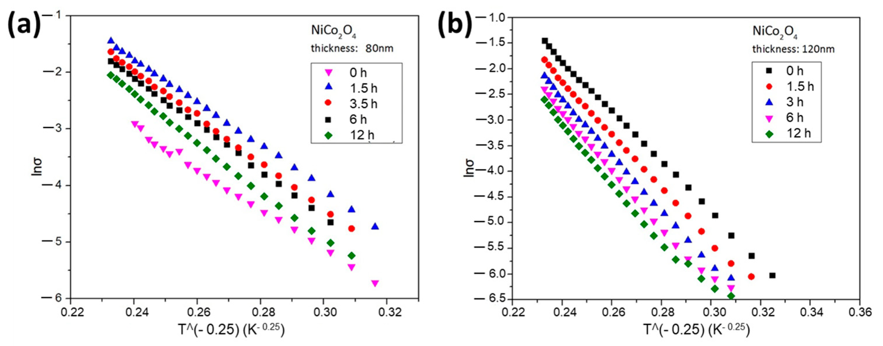
We investigated the electrical properties of the material using D.C. conductivity studies. The D.C. conductivity of NiCo2O4 films of 80 nm (Figure 1a) and 120 nm (Figure 1b) thickness was examined in the temperature range of 100 to 340 K. The thermal treatment of the samples took place at 340 K for 1.5, 3, 6, and 12 h. By increasing the time of thermal aging, a shift of the curve to lower conductivity values appears, which indicates that this “soft thermal treatment” has a measurable impact on the conductivity and is thus attributed to internal structural change.
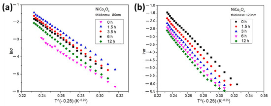
Figure 1.
The In σ = f(T−0.25) measurements for (a) 80 nm thickness of NiCo2O4 film and (b) 120 nm thickness of NiCo2O4 film, heated at 70 °C under ambient air conditions for aging times 0, 1.5, 3, 6 and 12 h, respectively.
The conductivity was thermally activated, and its dependence versus temperature is studied in the frame of Variable Range Hopping (VRH) and Nearest Neighbour Hopping (NNH). In Mott’s model, the hopping distance is given by , where the localization length and [25]. From the equation: , we can calculate the density of states N, , where T0 ~ 80 × 105 K. In such a case, taking T = 300 K, we find for the hopping distance: This value is about four times the lattice parameter, in good accordance to Dillep K. et al. [26].
The solution combustion synthesis of NiCo2O4 implies the formation of nanoparticles (NPs). The typical grain dimensions range from 3.5 to 5 nm without avoiding the presence of amorphous microregions [24]. The conductivity versus temperature measurements, in the range of 100–340 K, reveal a Mott’s conduction according to the formula: σ = σ0 exp [−(T0/T)0.25]. The same model also holds after heat treatment of the samples for t = 1.5, 3, 6, and 12 h. For the thinner nickel cobaltite film of 80 nm, a short heating of 1.5 h improves the conductivity, though longer heat treatment gradually displaces the conductivity curve to lower values (Figure 1a). For the thicker nickel cobaltite film of 120 nm, a monotonic decrease in the conductivity values occurs, indicating that the thickness exerts influence on the way that the thermal heating affects the internal structure of the material (Figure 1b).
In polycrystalline metal oxide films, the grain boundaries can act as deep traps and cause the film’s conductivity to decay or recover slowly. However, regarding NiCo2O4 films, Hu et al. 2011 have proposed that the aforementioned deep trap defect on the photo-response behavior has been avoided due to their short decay and recovery times, which may be attributed to their exceptional crystallinity, purity, and morphology of nanoparticles [27]. Due to the existence of physical boundaries between the NiCo2O4 nanoparticles, the charge transfer among them is “hopping-like” [28].
In general, a “hopping-like’’ transport is stated by the temperature dependency of the experimental measurements of the conductivity, where the parameter σ0 is a measure of the conductivity, which is related to the interior of the grains of the material. The parameter T0, on the contrary, is a measure of the potential barrier height, as thermally activated carriers hop between localized states with distinct energies [29,30].
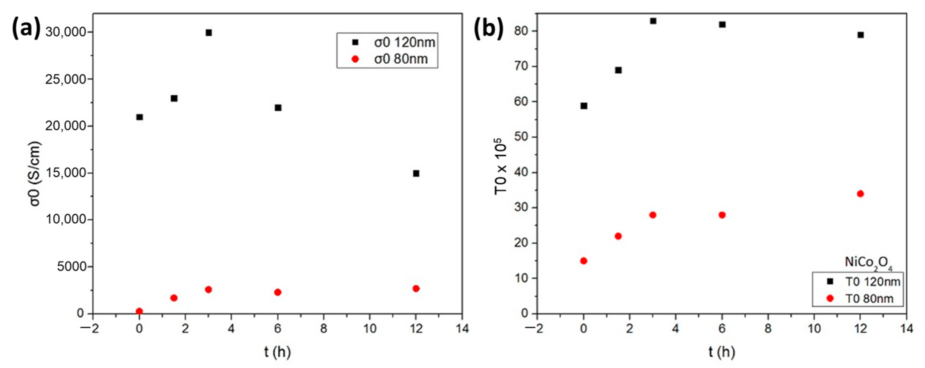
As seen in Figure 2, the values of σ0 and T0 increase after heat treatment at 70 °C during the first three hours for both nickel cobaltite films of 80 nm and 120 nm thickness, respectively. Specifically, regarding the thicker 120 nm NiCo2O4 film, it is depicted that the values of σ0 range from 21 × 103 S cm−1 for t = 0 h to 30 × 103 S cm−1 for t = 3 h, while the values of T0 increase from 59 × 105 K to 83 × 105 K, respectively. Similar behavior is observed for the thinner 80 nm NiCo2O4 film during the first three hours whilst depicting 12 times lower values of σ0 and about three times lower values of T0 for t = 3 h in comparison to the thicker 120 nm NiCo2O4 film (Figure 2a,b). This indicates that there is an improvement in conduction mechanisms during the first three hours following a stabilization of the process, remaining nearly constant during the thermal treatment exceeding four hours, suggesting that the conductivity, in that case, is not affected by thermal aging. The charge carrier mobility and concentration of the solution combustion synthesized NiCo2O4 were obtained using a 1T magnet. The p-type NiCo2O4 films exhibit a high carrier concentration of ~3.9 × 1020 cm−3 and a mobility of ~7.4 × 10⁻² cm2/V.s.
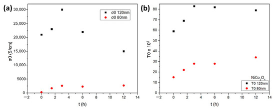
Figure 2.
The parameters (a) σ0 and (b) T0 versus the aging time for 80 nm thickness of NiCo2O4 film and 120 nm thickness of NiCo2O4 film, respectively, during thermal treatment at 70 °C under ambient air.
3.2. Normal Device Architecture OPVs with Neat NiCo2O4 and Cu-SCN Surface Modified NiCo2O4 HTLs
The above observation of suitable conductivity, low toxicity, and relatively low processing temperature of NiCo2O4 are important parameters for high-performance and environmentally friendly OPVs. In this section, we fabricate a normal device structure OPVs based on the T1:ITIC-4F active layer using NiCo2O4 and Cu-SCN surface-modified NiCo2O4 HTLs. Importantly, for the processing of the presented OPVs, the low-toxicity solvent O-xylene is used instead of commonly used, replacing the high-toxicity halogenated solvents (e.g., chloroform, chlorobenzene) commonly used for reporting high-performance OPVs in the literature. Furthermore, both NiCo2O4 and Cu-SCN surface-modified NiCo2O4 HTLs, as well as the OPV active layer, were deposited using blade coating, which is a scalable technique compatible with the fabrication of large-area OPVs.
Thus, the neat and Cu-SCN surface-modified NiCo2O4 HTLs were used as hole-transporting layers in OPVs with the following structure: ITO/HTL/T1:ITIC-4F/Ca/Al. Figure 3 presents the light J-V curves of the corresponding solar cells under 1 sun-simulated light (A.M.1.5) using neat NiCo2O4 and surface modified with Cu-SCN as HTLs. The respective photovoltaic parameters, open circuit voltage (Voc), short circuit current (Jsc), fill factor (FF), and power conversion efficiency (PCE) are presented in Table 1. The OPVs with neat NiCo2O4 HTL provide a PCE = 4.38%, with a Voc = 0.89 V, Jsc = 12.00 mA/cm2 and FF = 40.75%. The proposed Cu-SCN surface treatment of the NiCo2O4 improves the PV parameters: a Voc = 0.92 V, Jsc = 15.06 mA/cm2, and FF = 44.76% and thus improves the corresponding PCE value to 6.20%. The PCE enhancement is ascribed to the Cu-SCN surface treatment of the NiCo2O4 HTL that provides passivation of the surface defects of NiCo2O4, reducing the interface charge carrier recombination as it can be derived from the increased Voc value of the corresponding OPVs. Moreover, the Cu-SCN surface treatment of the NiCo2O4 HTL improves the electron-blocking properties of the bottom OPV electrode, resulting in increased Jsc and FF values for the corresponding OPVs. The above initial device performance results demonstrate the potential of NiCo2O4 and Cu-SCN surface-treated NiCo2O4 HTLs for the fabrication of environmentally friendly OPVs.
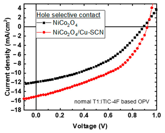
Figure 3.
Light J-V curves of T1:ITIC-4F based OPVs with NiCo2O4 (black square) and NiCo2O4/Cu-SCN (red cycles) as hole transporting layers.

Table 1.
PV parameters of the normal device architecture T1:ITIC-4F based OPV using NiCo2O4 and NiCo2O4/Cu-SCN as hole transporting layers.
4. Conclusions
In conclusion, we studied the electrical properties of NiCo2O4 films using D.C. conductivity and Hall effect measurements. The D.C. conductivity measurements via a soft thermal aging treatment of NiCo2O4 films of different thicknesses (80 and 120 nm) that have been processed to identical conditions to NiCo2O4 HTLs incorporated within OPVs showed a detectable impact on the conductivity, which was accredited to internal structural change. Specifically, for the thinner nickel cobaltite HTL of 80 nm, a short heating time of 1.5 h increased the conductivity, whereas a prolonged heating time gradually shifted the conductivity curve to lower values, whilst for the thicker nickel NiCo2O4 HTL of 120 nm, the conductivity values decreased monotonically. Those measurements enabled us to identify a “hopping-like” charge transport as the primary mechanism that determines the conductivity and consequently calculate the “hopping” distance of solution-processed nanoparticulate-based NiCo2O4 HTLs. Moreover, hall effect measurements revealed a high carrier concentration of ~3.9 × 1020 cm−3 and mobility of ~7.4 × 10⁻² cm2/V.s for p-type NiCo2O4 HTLs. Furthermore, we examined the implementation of low toxicity NiCo2O4 and Cu-SCN surface modified NiCo2O4 as hole transporting layers on the performance of non-fullerene acceptor (T1:ITIC-4F) based OPVs that have been processed by blade coating using non-chlorinated solvents such as O-xylene and alcohols, thus giving the opportunity for the development of eco-friendly solution-processed OPVs. The initial reported solar cell device results for the proposed Cu-SCN surface treatment of NiCo2O4 HTL showed improved photovoltaics characteristics, yielding Voc = 0.92 V, Jsc = 15.06 mA/cm2, and FF = 44.76%, and thus enhancing the corresponding PCE value to 6.20% compared to untreated NiCo2O4 HTL based OPVs with PCE of 4.38%.
Author Contributions
Conceptualization, S.A.C. and I.T.P.; methodology, A.I., A.K., D.K., E.C., S.S., E.V., S.A.C. and I.T.P.; formal analysis, A.I., A.K., D.K., E.C., S.S., E.V., S.A.C. and I.T.P.; investigation, A.I., A.K., D.K., E.C., S.S., E.V., S.A.C. and I.T.P.; data curation, A.I.; writing—original draft preparation, A.I., S.A.C. and I.T.P.; writing—review and editing, S.A.C. and I.T.P.; supervision, S.S., E.V., S.A.C. and I.T.P.; funding acquisition, S.A.C. All authors have read and agreed to the published version of the manuscript.
Funding
This research received no external funding.
Institutional Review Board Statement
Not applicable.
Informed Consent Statement
Not applicable.
Data Availability Statement
The data that support the findings of this study are available from the corresponding author upon reasonable request.
Conflicts of Interest
The authors declare no conflict of interest.
References
- Kannan, N.; Vakeesan, D. Solar energy for future world: A review. Renew. Sustain. Energy Rev. 2016, 62, 1092–1105. [Google Scholar] [CrossRef]
- ur Rehman, S.; Noman, M.; Khan, A.D.; Saboor, A.; Ahmad, M.S.; Khan, H.U. Synthesis of polyvinyl acetate/graphene nanocomposite and its application as an electrolyte in dye sensitized solar cells. Optik 2020, 202, 163591. [Google Scholar] [CrossRef]
- Lin, Y.; Shao, Y.; Dai, J.; Li, T.; Liu, Y.; Dai, X.; Xiao, X.; Deng, Y.; Gruverman, A.; Zeng, X.C.; et al. Metallic surface doping of metal halide perovskites. Nat. Commun. 2021, 12, 7. [Google Scholar] [CrossRef] [PubMed]
- Chen, Q.; Chen, L.; Ye, F.; Zhao, T.; Tang, F.; Rajagopal, A.; Jiang, Z.; Jiang, S.; Jen, A.K.Y.; Xie, Y.; et al. Ag-Incorporated Organic-Inorganic Perovskite Films and Planar Heterojunction Solar Cells. Nano Lett. 2017, 17, 3231–3237. [Google Scholar] [CrossRef]
- Georgiou, E.; Ioakeimidis, A.; Antoniou, I.; Papadas, I.T.; Hauser, A.; Rossier, M.; Linardi, F.; Choulis, S.A. Non-Embedded Silver Nanowires/Antimony-Doped Tin Oxide/Polyethylenimine Transparent Electrode for Non-Fullerene Acceptor ITO-Free Inverted Organic Photovoltaics. ACS Appl. Electron. Mater. 2023, 5, 181–188. [Google Scholar] [CrossRef]
- Hermerschmidt, F.; Choulis, S.A.; List-Kratochvil, E.J.W. Implementing Inkjet-Printed Transparent Conductive Electrodes in Solution-Processed Organic Electronics. Adv. Mater. Technol. 2019, 4, 1800474. [Google Scholar] [CrossRef]
- Park, S.; Kim, T.; Yoon, S.; Koh, C.W.; Woo, H.Y.; Son, H.J. Progress in Materials, Solution Processes, and Long-Term Stability for Large-Area Organic Photovoltaics. Adv. Mater. 2020, 32, 2002217. [Google Scholar] [CrossRef]
- Liu, S.; Yuan, J.; Deng, W.; Luo, M.; Xie, Y.; Liang, Q.; Zou, Y.; He, Z.; Wu, H.; Cao, Y. High-efficiency organic solar cells with low non-radiative recombination loss and low energetic disorder. Nat. Photonics 2020, 14, 300–305. [Google Scholar] [CrossRef]
- Zhu, L.; Zhang, M.; Xu, J.; Li, C.; Yan, J.; Zhou, G.; Zhong, W.; Hao, T.; Song, J.; Xue, X.; et al. Single-junction organic solar cells with over 19% efficiency enabled by a refined double-fibril network morphology. Nat. Mater. 2022, 21, 656–663. [Google Scholar] [CrossRef]
- Bao, S.; Yang, H.; Fan, H.; Zhang, J.; Wei, Z.; Cui, C.; Li, Y. Volatilizable Solid Additive-Assisted Treatment Enables Organic Solar Cells with Efficiency over 18.8% and Fill Factor Exceeding 80%. Adv. Mater. 2021, 33, 2105301. [Google Scholar] [CrossRef]
- Po, R.; Carbonera, C.; Bernardi, A.; Camaioni, N. The role of buffer layers in polymer solar cells. Energy Environ. Sci. 2011, 4, 285–310. [Google Scholar] [CrossRef]
- Li, Y.; Huang, X.; Ding, K.; Sheriff, H.K.M.; Ye, L.; Liu, H.; Li, C.-Z.; Ade, H.; Forrest, S.R. Non-fullerene acceptor organic photovoltaics with intrinsic operational lifetimes over 30 years. Nat. Commun. 2021, 12, 5419. [Google Scholar] [CrossRef] [PubMed]
- Georgiou, E.; Papadas, I.T.; Antoniou, I.; Oszajca, M.F.; Hartmeier, B.; Rossier, M.; Luechinger, N.A.; Choulis, S.A. Antimony doped tin oxide/polyethylenimine electron selective contact for reliable and light soaking-free high performance inverted organic solar cells. APL Mater. 2019, 7, 91103. [Google Scholar] [CrossRef]
- Ioakeimidis, A.; Hauser, A.; Rossier, M.; Linardi, F.; Choulis, S.A. High-performance non-fullerene acceptor inverted organic photovoltaics incorporating solution processed doped metal oxide hole selective contact. Appl. Phys. Lett. 2022, 120, 233301. [Google Scholar] [CrossRef]
- Sorrentino, R.; Kozma, E.; Luzzati, S.; Po, R. Interlayers for non-fullerene based polymer solar cells: Distinctive features and challenges. Energy Environ. Sci. 2021, 14, 180–223. [Google Scholar] [CrossRef]
- Shrotriya, V.; Li, G.; Yao, Y.; Chu, C.W.; Yang, Y. Transition metal oxides as the buffer layer for polymer photovoltaic cells. Appl. Phys. Lett. 2006, 88, 73508. [Google Scholar] [CrossRef]
- Irwin, M.D.; Buchholz, D.B.; Hains, A.W.; Chang, R.P.H.; Marks, T.J. p-Type semiconducting nickel oxide as an efficiency-enhancing anode interfacial layer in polymer bulk-heterojunction solar cells. Proc. Natl. Acad. Sci. USA 2008, 105, 2783–2787. [Google Scholar] [CrossRef]
- Han, S.; Shin, W.S.; Seo, M.; Gupta, D.; Moon, S.J.; Yoo, S. Improving performance of organic solar cells using amorphous tungsten oxides as an interfacial buffer layer on transparent anodes. Org. Electron. 2009, 10, 791–797. [Google Scholar] [CrossRef]
- Wang, K.; Ren, H.; Yi, C.; Liu, C.; Wang, H.; Huang, L.; Zhang, H.; Karim, A.; Gong, X. Solution-processed Fe3O4 magnetic nanoparticle thin film aligned by an external magnetostatic field as a hole extraction layer for polymer solar cells. ACS Appl. Mater. Interfaces 2013, 5, 10325–10330. [Google Scholar] [CrossRef]
- Yu, Z.; Liu, W.; Fu, W.; Zhang, Z.; Yang, W.; Wang, S.; Li, H.; Xu, M.; Chen, H. An aqueous solution-processed CuOX film as an anode buffer layer for efficient and stable organic solar cells. J. Mater. Chem. A 2016, 4, 5130–5136. [Google Scholar] [CrossRef]
- Gama, L.; Ribeiro, M.A.; Barros, B.S.; Kiminami, R.H.A.; Weber, I.T.; Costa, A.C.F.M. Synthesis and characterization of the NiAl2O4, CoAl2O4 and ZnAl2O4 spinels by the polymeric precursors method. J. Alloys Compd. 2009, 483, 453–455. [Google Scholar] [CrossRef]
- Xu, H.; Xu, H.; Yuan, F.; Zhou, D.; Liao, X.; Chen, L.; Chen, Y.; Chen, Y. Hole transport layers for organic solar cells: Recent progress and prospects. J. Mater. Chem. A 2020, 8, 11478–11492. [Google Scholar] [CrossRef]
- Wu, Z.; Zhu, Y.; Ji, X. NiCo2O4-based materials for electrochemical supercapacitors. J. Mater. Chem. A 2014, 2, 14759–14772. [Google Scholar] [CrossRef]
- Papadas, I.T.; Ioakeimidis, A.; Armatas, G.S.; Choulis, S.A. Low temperature combustion synthesis of a spinel NiCo2O4 hole transport layer for perovskite photovoltaics. Adv. Sci. 2018, 5, 1701029. [Google Scholar] [CrossRef] [PubMed]
- Dalas, E.; Mougoyannis, P.; Sakkopoulos, S. Εffect of ΖnO concentration on the structure and charge transport in conductive polypyrrole/ΖnO x% w/w composites with x = 10, 20, 30 and 40. Rom. J. Phys. 2013, 58, 354–364. [Google Scholar]
- Dileep, K.; Loukya, B.; Silwal, P.; Gupta, A.; Datta, R. Probing optical band gaps at nanoscale from tetrahedral cation vacancy defects and variation of cation ordering in NiCo2O4 epitaxial thin films. J. Phys. D Appl. Phys. 2014, 47, 405001. [Google Scholar] [CrossRef]
- Hu, L.; Wu, L.; Liao, M.; Fang, X. High-performance NiCo2O4 nanofilm photodetectors fabricated by an interfacial self-assembly strategy. Adv. Mater. 2011, 23, 1988–1992. [Google Scholar] [CrossRef]
- Hu, L.; Wu, L.; Liao, M.; Hu, X.; Fang, X. Electrical transport properties of large, individual NiCo2O4 nanoplates. Adv. Funct. Mater. 2012, 22, 998–1004. [Google Scholar] [CrossRef]
- Vitoratos, E.; Sakkopoulos, S.; Dalas, E.; Paliatsas, N.; Karageorgopoulos, D.; Petraki, F.; Kennou, S.; Choulis, S.A. Thermal degradation mechanisms of PEDOT:PSS. Org. Electron. 2009, 10, 61–66. [Google Scholar] [CrossRef]
- Vitoratos, E.; Sakkopoulos, S.; Dalas, E.; Emmanouil, K. Conductivity Degradation Study of polypyrrole and polypyrrole/5% w/w TiO2 nanocomposite under Heat Treatment in Helium and Atmospheric Air. Int. J. Eng. Appl. Sci. 2016, 3, 13–16. [Google Scholar]

Disclaimer/Publisher’s Note: The statements, opinions and data contained in all publications are solely those of the individual author(s) and contributor(s) and not of MDPI and/or the editor(s). MDPI and/or the editor(s) disclaim responsibility for any injury to people or property resulting from any ideas, methods, instructions or products referred to in the content. |
© 2023 by the authors. Licensee MDPI, Basel, Switzerland. This article is an open access article distributed under the terms and conditions of the Creative Commons Attribution (CC BY) license (https://creativecommons.org/licenses/by/4.0/).