
An Electron Waveguide Model for FDSOI Transistors

Department of Computational Physics, Brandenburg Technical University Cottbus/Senftenberg, P.O. Box 101344, 03013 Cottbus, Germany
Solids 2022, 3(2), 203-218; https://doi.org/10.3390/solids3020014
Submission received: 27 February 2022
/
Revised: 30 March 2022
/
Accepted: 6 April 2022
/
Published: 15 April 2022
(This article belongs to the Special Issue Solids in Europe)
Abstract
:We extend our previous semi-empirical model for quantum transport in a conventional nano-MOSFET to FDSOI transistors. In ultra-thin-body and -BOX (UTBB) FDSOI transistors, the electron channel can be treated as an electron waveguide. In the abrupt transition approximation, it is possible to derive an analytical approximation for the potential seen by the charge carriers. With these approximations we calculate the threshold voltage and the transfer characteristics, finding remarkably good agreement with experiments in the OFF-state given the relative simplicity of our model. In the ON-state, our theory fails because Coulomb interaction between the free charge carriers and the device heating is neglected in our approach.
1. Introduction
The notion of electron waveguide transport was used in the late 1980s and in the 1990s to discuss split-gate AlGaAs/GaAs devices [1,2]. The initiating observation in this field was the observation of quantized conduction in a point contact [3,4]. The electron waves in the waveguide are the quantum mechanical wave functions resulting from the Schrödinger equation, which are assumed to be coherent in the entire device. In a wave guide, transport is subjected to a two-dimensional potential perpendicular to the transport direction and leading to global transverse modes. Here we present a model for a FDSOI transistor in which its conduction channel is treated as an electron waveguide (FD—fully depleted, SOI—silicon-on insulator; for a review, see [5]). The model is formulated so that it can be generalized to other modern transistor architectures such as FinFETs, horizontal and vertical Nanowire transistors, and Nanosheet FETs in which the conduction channel takes a similar form [6].
For the transverse modes of an electron waveguide to be observable, essentially three conditions have to be fulfilled [2]: (i) The scale of the transverse confinement must be at most comparable to the Fermi wave length; (ii) The dimensions of the conduction channel have to be smaller than the elastic and inelastic scattering lengths; and (iii) The differences of the energies of the transverse modes must be larger than the thermal energy and larger than , where is the applied drain voltage.
In a series of studies [7,8,9,10], we developed a compact semi-empirical model for quantum transport in a conventional nano-MOSFET in which the experimental output characteristics could be described quantitatively. In this study, we extend this model to thin body transistors focusing on ultra-thin-body and -BOX (UTBB) FDSOI transistors with a back plane (BP) as a back gate [5,11,12,13,14,15,16,17,18,19]. Typically, in a UTBB FDSOI transistor the threshold voltage (VT) is adjusted by the work function of the metal gate, the polarity of the BP-doping, and the back gate bias allowing multi-VT operation [5,18]: High-VT (HVT) devices allow for low-leakage currents and low power dissipation whereas standard-VT (SVT) and low-VT (LVT) devices allow for fast operation. Because of the ultra-thin-body it is possible to define in the considered devices global transverse modes without mode coupling, thus simplifying more complex T-matrix type approaches with inherent mode coupling as in References [20,21,22,23,24,25].
In general, Coulomb interaction between the free charge carriers and device heating play an important role in thin film devices [26,27,28,29,30,31]. However, here we focus on the threshold- and sub-threshold regime which are of particular importance for CMOS-technology. Therefore, we may neglect these effects. It is thus possible to derive an analytical understanding of a number of the aspects of the transistor. Compared to experiments by [18], we find reasonable agreement. We also discuss to what extent the electron waveguide conditions i–iii are met in the considered UTBB FDSOI transistors.
2. Materials and Methods
2.1. Quantum Transport Model
We consider a multiple VT, fully depleted SOI-transistor with a back plane (BP), as depicted in Figure 1. The n-conduction channel (waveguide) is located in a thin, nearly undoped active Si-layer of thickness D (’thin body’) and width W. The conduction channel is sandwiched between the source- and the drain contact, which are heavily n-doped. The bottom side of the active Si-layer is terminated by an insulating SiO2-layer (BOX). Below lies the BP consisting either of a heavily p- or a heavily n-doped silicon layer. The back contact with voltage is connected to the BP via a p-doped region (’p-well’). Further abbreviations are HK-MG for the high-k/metal gate stack and STI for shallow trench insulation. Outside the active Si-layer, the wave functions of the current carrying electrons vanish, leading to the boundary condition
(Definition of the coordinates. Figure 1b.) In the active layer with -orientation (Figure 1d), we start from the single particle Schrödinger equation
Here we assume isotropy in the z-direction (width direction). In the bulk semiconductor there are six equivalent valleys , which in the finite Si-layers are split into three classes (Figure 1): First with , , second, with , , and, third, with , . Here is the large effective mass and is the small effective mass associated with the constant energy ellipsoids of the valleys.
If the thickness of the Si-layer is small, one can approximate by its average defined by
so that
(see Figure 2b,c). Because of good screening in the contacts we can write and leading to
The effective potential in the scattering area will be discussed in Section 2.2. The independence of the potential (4) of the transverse coordinates allows for a product ansatz
for the wave functions which correspond to electron states in an electron wave guide. Here the global transverse modes are given by
The factor describes the propagation of a charge carrier in this mode since the total energy E is split in a transverse energy of the motion in the y-z-direction
and a longitudinal energy
of the motion in the x-direction. Insertion of (6) into (4) leads to the one-dimensional scattering problem
The source-incident scattering solutions exhibit the asymptotic
and
Here the wave number is given by
with for the source and for the drain as well as and . Our method for the numerical evaluation of the transmission coefficients is described in detail in Appendix E of [10].
The drain current results from the contributions of the six valleys according to given by the Landauer–Büttiker formula. As we discuss in detail in Appendix A:
Here the one-dimensional current transmission is given by
In the limit of large W, the supply function is given by
with the Fermi–Dirac integral
The calculation of the chemical potential is demonstrated in Appendix B. The total current per width is determined from (14) according to
2.2. Potential in Abrupt Transition Approximation
For the potential in the Si-film entering into (2), we can write in the contacts and . In the conduction channel, i.e., for it can be found from Poisson’s equation
with the charge density and appropriate boundary conditions. Here, is the vacuum permitivity and is given by the dielectric constant of the high-k-dielectric, is given by the dielectric constant of the Si-film, and is given by the dielectric constant in the BOX. As shown in Figure 1a, marks the interface between top-gate insulation and top gate and marks the interface between BOX and back gate (BP). For the conduction channel, we specialize Equation (19) to the threshold- and sub-threshold regime, which is important for technological applications. Here, we may neglect the contribution of the free charge carriers. In FDSOI technology, one assumes furthermore the full ionization of the impurities (depletion approximation) so that with the acceptor density in the Si-layer. One finds
This equation was studied, e.g., in References [32,33,34,35,36]. To construct a potential approximation of the form as assumed in Equation (4), we here apply the abrupt transition-approximation as described in References [9,10]. While in the contacts we have and , there is an abrupt transition to the potential in the scattering area (, conduction channel). In the scattering area, we seek a solution of (20) of the separable form
and then construct according to (3)
In the latter expression we assume for a thin film that the quantization energy induced by the boundary condition is dominant over the potential variation of so that we can replace with its average, . Upon insertion of (21) into (20), one obtains
We now impose Dirichlet boundary conditions
As usual, the flat band energies
are defined by the difference between the chemical potential in the grounded source and the chemical potential in the respective isolated contact, for the top gate and for the back gate. Then, one has for the electro chemical potential in the top gate for the value as required. Furthermore, we require at the two silicon-insulator interfaces at and the usual continuities of and , resulting in
plus corresponding relations at . As is characteristic for the abrupt transition-approximation, the potential in (21) can be interpreted as the superposition of, first, a constant electric field in longitudinal direction, , induced by the drain voltage and, second, a transverse potential variation describing an infinite conduction channel at .
3. Results
Theoretical parameters: With the exception of Figure 3 where we vary the parameter , we use the parameters nm, nm, nm, , , ( is the equivalent oxide thickness EOT), nm, , K, (-doping in source and drain), (weak p-doping in conduction channel), and the operating voltage of V. These parameters are compatible with the ones in Reference [18]. From Equation (A15), one obtains a value of eV. As shown in the energy diagrams of the isolated contacts in Figure 2a, we take the bottom of the conduction band in the grounded -source as the energy zero. For the chemical potential in the isolated gate metal, we choose eV, which is the mid gap position in silicon. For the back gate one assumes a doping concentration markedly lower than that of the -source ( in Reference [18]) corresponding to eV for an n-BP and V for a p-BP. For the flat band voltages, it follows from (25)
(See Figure 2a.) As an example, we consider in Figure 2 an n-channel transistor with an n-BP at . In part (b), the transverse potential is plotted as calculated from Equations (27)–(29). In the limit of small D, it is permissible to set (for discussion, see Equation (A30)) so that in (28) the curvature of the potential in the conduction channel can be neglected. In consequence, is close to a piecewise linear function across the silicon layer. The transverse ideal box-confinement induced by the boundary condition in Equation (1) causes a typical quantization energy in the corresponding ideal box-confinement given by
at nm, were is the effective band mass. We compare this energy to the absolute value of the total change of across the conduction channel as taken from Figure 2b. This change is maximum at , taking the value meV. Therefore, holds, where is the excitation energy from the first to the second lowest level of the quantization in the y-direction. This relation justifies the transition from Equation (2) to Equation (4). Comparing to meV at room temperature, it is seen that condition (iii) for the observability of the transverse modes listed in the introduction is fulfilled. Setting and , one obtains nm. So condition (i) is almost fulfilled, especially if one takes smaller values for . Condition (ii) probably requires shorter channels.
In Figure 2c, the effective barrier height according to Equation (33) is shown. In the limit , one obtains a linear relation given by
with
and
(see Appendix D). Because , the parameter A is small, for our system taking the value , so that .
In Figure 2c, we also plot the threshold voltage (in text abbreviated with VT) as calculated from the condition
This condition was used in earlier studies for a conventional MOSFET (see, for example, Figure 4 of [9]).
An important feature of the FDSOI technology is the possibility to control the threshold gate voltage, first, by choosing either an n-BP or a p-BP, and, second, by applying a voltage at the BP. Important VT-options are listed in Table 1 of [16]:
- n-BP with : standard-VT (SVT (i)), identical with Figure 2b;
- n-BP with : low-VT (LVT);
- p-BP with : high-VT (HVT);
- p-BP with standard-VT (SVT (ii)).
The associated effective barrier heights are given in Figure 4. From Equation (36), one finds in all four cases a good linear approximation with identical slopes . A further inspection of Equation (36) reveals that equal barrier heights for SVT(ii) and SVT(i) result from the identical value . In the general case, one obtains identical results for SVT(i) and SVT(i) if
where is the difference between the flat band energies in the p-BP and the n-BP.
In Figure 3, we plot the threshold voltage calculated from condition (39) with the linear approximation of , as given in Equation (36) so that
We find reasonable agreement with the experimental results in Figure 3 of [18]. In Appendix D, it is shown that (41) can be simplified to give
In Figure 3 it is demonstrated that the expressions (41) and (42) agree very closely. According to Equation (42), we find for the value for corresponding to mid-gap position. From Figure 3 of [18], we read for the experimental value mV, which might indicate a shift of the experimental from mid-gap position. The formula (42) explains the finding , which is present in experiments as well. Note that in theory and experiments, the identical curves for SVT(i) and for SVT(ii) both bend up slightly.
In Figure 5 we plot the transfer characteristics resulting in the four VT-options. As documented in Table 1, we find for the threshold- and subthreshold regime a remarkable agreement between theory and experiment in view of the simplifications in our theory. The major simplifications are the use of the abrupt transition approximation, the neglect of Coulomb interaction of the free carriers, and the disregard of the x-dependence of . It can be expected that without abrupt transition approximation, the transition between contacts and conduction channel is smoothed out and the maximum of the barrier is shifted from towards the interior of the conduction channel. Because of the longitudinal electric field in the conduction channel, the height of the barrier will then be reduced, leading to the well-known drain induced barrier lowering (DIBL). This effect can explain the higher theoretical values for . As can be expected, in the ON-state our model fails. The first reason is the neglect of the free carriers in the charge density entering into the Poisson equation (20). Above threshold free carriers increasingly enter the conduction channel and alter the potential because of screening. The second reason is heating, which has been neglected in our approach but which becomes substantial above threshold. The third reason is the neglect of the linear drop of , which becomes important in the ON-state when .
4. Discussion
The presented theoretical model for a FDSOI transistor has been designed on the one hand to be complex enough to enter all relevant physical parameters and on the other hand to be simple enough to allow for an analytical discussion as much as possible. It is designed for the threshold- and sub-threshold regime. Here, the theoretical results are remarkably close to the experimental ones. The model fails completely in the ON-state regime. Here, Coulomb interaction between the charge carriers and device heating becomes important [9] as well as the linear drop in . These have been neglected in our model and have to be included in future work.
Funding
This research received no external funding.
Data Availability Statement
Not applicable.
Conflicts of Interest
The author declares no conflict of interest.
Abbreviations
The following abbreviations are used in this manuscript:
| MDPI | Multidisciplinary Digital Publishing Institute |
| DOAJ | Directory of open access journals |
| TLA | Three letter acronym |
| LD | Linear dichroism |
Appendix A. Adoption of a Previous Transistor model for the Calculation of the Drain Current
The transistor model in Section 4 of Reference [10], including conditions P1–P6, can be directly applied to the model for an SOI-transistor in Section 2.1. The waveguide geometry of the conduction channel in Figure 1b is identical with the geometry in Figure 2b of [10]. The potentials in the source and in the drain are identical. The global transverse modes arise from the separable potential in Equation (21), identical with Equations (35) and (36) The notation ’equation (…)’ we use for equations is in Reference [10]. The further thin-film approximation in Equation (22) corresponds to the setting in Equation (35) and . The single transverse mode approximation condition P7 is introduced in Section 3. Because of the simple form of the transverse potential , one has in P5 the planarity in the two transverse directions so that two global transverse coordinates y and z exist and . The longitudinal coordinates are for the source and for the drain. Because of , the transverse functions in the conduction channel and the transverse functions in the contacts in Reference [10] coincide, having identical transverse mode energies,
Combining Equations (11), (12), and (6), the asymptotics of the source-incident scattering function take the form
and
Comparing with Equation (4), we obtain the relation
Then, from Equation (8) one obtains the current transmission sum
with the one-dimensional current transmission given by Equation (15). From Equation (7), we find Equation (14)
For or , the supply function is given by
with the Fermi–Dirac integral
In the last step we made use of Equations (70)–(73) occur in Reference [10] which hold in the limit . In the OFF-state, only the high-energy tail of the Fermi-distribution contributes significantly and a Boltzmann approximation can be introduced
Appendix B. The Chemical Potential in Source and Drain
We assume identical cubic source/drain contacts of length in the x-direction, D in the y-direction, and W in the z-direction. To calculate , we write the number of free charge carriers in the source contact
with . Here, we assume fixed boundary conditions in all space directions and include spin degeneracy with a factor of two. Introducing the free carrier density n with , one finds from (A10) in the limit and setting and
Here, we assume full ionization of the donors so that with the donor concentration equal in source and drain. Define
to write
where we have included a quarter circle with radius R only. With it follows that
with . The integral can be carried out analytically
From this identity the chemical potential can be calculated.
Appendix C. Solution of the Poisson Equation
- The matching condition leads to
- The matching condition leads to
- The matching condition leads to
- The matching condition leads to
Equations (A22)–(A25) constitute four inhomogeneous linear equations for the unknown variables , , and . Equations (A22) and (A23) allow for the elimination of to find
Inserting from (A26) yields
It follows that
We examine the curvature term in a SOIFET. Setting nm and assuming weak doping it follows that
In a thin body () FD SOI-FET with weak doping, the curvature term can be neglected.
Appendix D. Analytical Approximations for the Barrier Haight and the Threshold Voltage
We derive Equations (36) and (42): The barrier height as calculated from (33). In the limit it results from Equation (33)
with
and
If the parameter A is small, allowing a first order expansion in A
In the second step we take the limit , so that .
References
- Eugster, C.C.; del Alamo, J. Tunneling spectroscopy of an electron waveguide. Phys. Rev. Lett. 1991, 67, 3586. [Google Scholar] [CrossRef] [PubMed]
- Eugster, C.C.; del Alamo, J. Electron waveguide devices. Superlattices Microstruct. 1998, 23, 121–137. [Google Scholar]
- van Wees, B.J.; van Houten, H.; Beenakker, C.W.J.; Williamson, J.G.; Kouwenhoven, L.P.; van der Marel C., T. Foxon, D. Quantized conductance of point contacts in a two-dimensional. Phys. Rev. Lett. 1988, 60, 848. [Google Scholar] [CrossRef] [PubMed] [Green Version]
- Wharam, D.A.; Thornton, T.H.; Newbury, R.; Pepper, M.; Ahmed, H.; Frost, J.E.F.; Hasko, D.G.; Peacock, D.C.; Ritchie, D.A.; Jones, G.A.C. One-dimensional transport and the quantisation of the ballistic resistance. J. Phys. C 1988, 21, L209. [Google Scholar] [CrossRef]
- Cheng, K.; Khakifirooz, A. Fully depleted SOI (FDSOI) technology. Sci. China Inf. Sci. 2016, 59, 61402. [Google Scholar] [CrossRef] [Green Version]
- Pandey, A. Recent Trends in Novel Semiconductor Devices. Silicon 2022. [Google Scholar] [CrossRef]
- Nemnes, G.A.; Wulf, U.; Racec, P.N. Nano-transistors in the Landauer-Büttiker formalism. J. Appl. Phys. 2004, 96, 596–604. [Google Scholar] [CrossRef]
- Nemnes, G.A.; Wulf, U.; Racec, P.N. Nonlinear I-V characteristics of nanotransistors in the Landauer-Büttiker formalism. J. Appl. Phys. 2005, 98, 084308. [Google Scholar] [CrossRef]
- Wulf, U.; Kučera, J.; Richter, H.; Horstmann, M.; Wiatr, M.; Höntschel, J. Channel engineering for nanotransistors in a semiempirical quantum transport model. Mathematics 2017, 5, 68. [Google Scholar] [CrossRef] [Green Version]
- Wulf, U. A One-Dimensional Effective Model for Nanotransistors in Landauer-Büttiker Formalism. Micromachines 2020, 11, 359. [Google Scholar] [CrossRef] [Green Version]
- Horstmann, M.; Greenlaw, D.; Feudel, T.; Wei, A.; Frohberg, K.; Burbach, G.; Gerhardt, M.; Lenski, M.; Stephan, R.; Wieczorek, K.; et al. Sub-50 nm gate length SOI transistor development for high performance microprocessors. Mater. Sci. Eng. B 2004, 114, 3–8. [Google Scholar] [CrossRef]
- Numata, T.; Irisawa, T.; Tezuka, T.; Koga, J.; Hirashita, N.; Usuda, K.; Toyoda, E.; Miyamura, Y.; Tanabe, A.; Sugiyama, N.; et al. Performance enhancement of partially and fully depleted strained-SOI MOSFETs. IEEE Trans. Electron Devices 2006, 53, 1030–1038. [Google Scholar] [CrossRef]
- Fenouillet-Beranger, C.; Denormel, S.; Icard, B.; Boeuf, F.; Coignus, J.; Faynot, L.; Brevard, L.; Buj, C.; Soonekindt, C.; Todeschini, J.; et al. Fully-Depleted SOI Technology using High-K and Single-Metal Gate for 32 nm Node LSTP Applications featuring 0.179 μm2 6T-SRAM bitcell. In Proceedings of the 2007 IEEE International Electron Devices Meeting (IEDM), Washington, DC, USA, 10–12 December 2007. [Google Scholar]
- Fenouillet-Beranger, C.; Thomas, O.; Perreau, P.; Noel, J.P.; Bajolet, A.; Haendler, S.; Tosti, L.; Barnola, S.; Beneyton, R.; Perrot, C.; et al. Efficient Multi-VT FDSOI technology with UTBOX for low power circuit design. In Proceedings of the 2010 Symposium on VLSI Technology (VLSIT), Honolulu, HI, USA, 15–17 June 2010. [Google Scholar]
- Cheng, K.; Khakifirooz, A.; Kulkarni, P.; Edge, L.F.; Reznicek, A.; Adam, T.; He, H.; Seo, S.C.; Kanakasabapathy, S.; Schmitz, S.; et al. Challenges and Solutions of Extremely Thin SOI (ETSOI) for CMOS Scaling to 22 nm Node and Beyond. ECS Trans. 2010, 27, 951. [Google Scholar] [CrossRef]
- Liu, Q.; Monsieur, F.; Kumar, A.; Yamamoto, T.; Yagishita, A.; Kulkarnic, P.; Ponoth, S.; Loubet, N.; Cheng, K.; Khakifirooz, A.; et al. Impact of back bias on ultra-thin body and BOX (UTBB) devices. In Proceedings of the 2011 Symposium on VLSI Technology—Digest of Technical Papers, Kyoto, Japan, 14–16 June 2011. [Google Scholar]
- Skotnicki, T. Competitive SOC with UTBB SOI. In Proceedings of the 2011 IEEE International SOI Conference (SOI), Tempe, AZ, USA, 3–6 October 2011. [Google Scholar]
- Noel, J.; Thomas, O.; Jaud, M.A.; Weber, O.; Poiroux, T.; Fenouillet-Beranger, C.; Rivallin, P.; Scheiblin, P.; Andrieu, F.; Vinet, M.; et al. Multi-VT UTBB FDSOI Device Architectures for Low-Power CMOS Circuit. IEEE Trans. Electron Divices 2011, 58, 2473–2482. [Google Scholar] [CrossRef]
- Doris, B.; DeSalvo, B.; Cheng, K.; Morin, P.; Vinet, M. Planar Fully-Depleted-Silicon-On-Insulator technologies: Toward the 28 nm node and beyond. Solid-State Electron. 2016, 117, 37–59. [Google Scholar] [CrossRef]
- Venugopal, R.; Ren, Z.; Datta, S.; Lundstrom, M.S.; Jovanovic, D. Simulating quantum transport in nanoscale transistors: Real versus mode-space approaches. J. Appl. Phys. 2002, 92, 3730–3739. [Google Scholar] [CrossRef]
- Venugopal, R.; Goasguen, S.; Datta, S.; Lundstrom, M.S. Quantum mechanical analysis of channel access geometry and series resistance in nanoscale transistors. J. Appl. Phys. 2004, 95, 292–305. [Google Scholar] [CrossRef] [Green Version]
- Wang, J.; Polizzi, E.; Lundstrom, M. A three-dimensional quantum simulation of silicon nanowire transistors with the effective-mass approximation. J. Appl. Phys. 2004, 96, 2192–2203. [Google Scholar] [CrossRef] [Green Version]
- Polizzi, E.; Abdallah, N.B. Subband decomposition approach for the simulation of quantum electron transport in nanostructures. J. Comput. Phys. 2005, 202, 150–180. [Google Scholar] [CrossRef]
- Luisier, M.; Schenk, A.; Fichtner, W. Quantum transport in two- and three-dimensional nanoscale transistors: Coupled mode effects in the nonequilibrium Green’s function formalism. J. Appl. Phys. 2006, 100, 043713. [Google Scholar] [CrossRef] [Green Version]
- Vyurkov, V.; Semenikhin, I.; Filippov, S.; Orlikovsky, A. Quantum simulation of an ultrathin body field-effect transistor with channel imperfections. Solid State Electron. 2012, 70, 106–113. [Google Scholar] [CrossRef]
- Chu, Y.; Sarangapani, P.; Charles, J.; Klimeck, G.; Kubis, T. Explicit screening full band quantum transport model for semiconductor nanodevices. J. Appl. Phys. 2018, 123, 244501. [Google Scholar] [CrossRef]
- Chu, Y.; Lu, S.-C.; Chowdhury, N.; Povolotskyi, M.; Klimeck, G.; Mohamed, M.; Palacios, T. Superior Performance of 5-nm Gate Length GaN Nanowire nFET for Digital Logic Applications. IEEE Electron. Device Lett. 2019, 40, 874–877. [Google Scholar] [CrossRef]
- Martinez, A.; Barker, J.R. Quantum Transport in a Silicon Nanowire FET Transistor: Hot Electrons and Local Power Dissipation. Materials 2020, 13, 3326. [Google Scholar] [CrossRef]
- Sun, B.; Richstein, B.; Liebisch, P.; Frahm, T.; Scholz, S.; Trommer, J.; Mikolajick, T.; Knoch, J. On the Operation Modes of Dual-Gate Reconfigurable Nanowire Transistors. IEEE Trans. Electron. Devices 2021, 68, 3684–3689. [Google Scholar] [CrossRef]
- Prakash, O.; Dabhi, C.K.; Chauhan, Y.S.; Amrouch, H. Transistor Self-Heating: The Rising Challenge for Semiconductor Testing. In Proceedings of the 2021 IEEE 39th VLSI Test Symposium (VTS), San Diego, CA, USA, 25–28 April 2021. [Google Scholar]
- Liu, R.; Li, X.; Sun, Y.; Li, F.; Shi, Y. Thermal Coupling Among Channels and Its DC Modeling in Sub-7-nm Vertically Stacked Nanosheet Gate-All-Around Transistor. IEEE Trans. Electron. Devices 2021, 68, 6563–6570. [Google Scholar] [CrossRef]
- Young, K.K. Short-channel effect in fully depleted SOI MOSFETs. IEEE Trans. Electron. Devices 1989, 36, 399–402. [Google Scholar] [CrossRef]
- Yan, R.H.; Ourmazd, A.; Lee, K.F. Scaling the Si MOSFET: From bulk to SOI to bulk. IEEE Trans. Electron. Devices 1992, 39, 1704–1710. [Google Scholar] [CrossRef] [Green Version]
- Tsormpatzoglou, A.; Dimitriadis, C.A.; Clerc, R.; Rafhay, Q.; Panannakakis, G.; Ghibaudo, G. Semi-Analytical Modeling of Short-Channel Effects in Si and Ge Symmetrical Double-Gate MOSFETs. IEEE Trans. Electron. Devices 2007, 54, 1943–1952. [Google Scholar] [CrossRef]
- Mohammadi, H.; Abdullah, H.; Dee, V.F. A review on modeling the channel potential in multi-gate MOSFETs. Sains Malays. 2014, 43, 861–866. [Google Scholar]
- Li, X.; Ma, L.; Ai, Y.; Han, W. From parabolic approximation to evanescent mode analysis on SOI MOSFET. J. Semicond. 2017, 38, 024005. [Google Scholar] [CrossRef]
Figure 1.
(a) N-channel multiple VT, fully depleted SOI-transistor with a back plane (BP) (see text). (b) Active Si-layer for the conduction channel taking the form of a waveguide. (c) One-dimensional effective potential after Equation (22). (d) The (100)-orientation of the active Si-layer with the six constant energy ellipsoids .

Figure 2.
For the theoretical parameter set listed at the beginning of Section 3: (a) Energy diagrams of the isolated contacts. (b) Transverse confinement potential for an n-BP at (SVT(i)) for = 0.0 (black), 0.1 V (red), 0.2 V (green), 0.3 V (blue), 0.4 V (orange), 0.5 V (brown), 0.6 V (grey), 0.7 V (violet), 0.8 V (cyan), and 0.9 V (magenta). (c) In circles: Effective barrier height resulting from Equation (33), color coding as in part (b). Marked by an arrow: Threshold gate voltage determined by condition (39).

Figure 3.
The threshold voltage versus thickness of the box: n-BP with (orange), n-BP with (red), p-BP with (blue), and p-BP with (green). Solid lines according to Equation (41) and dashed lines according to Equation (42). The circles mark the values for nm which enter Table 1.
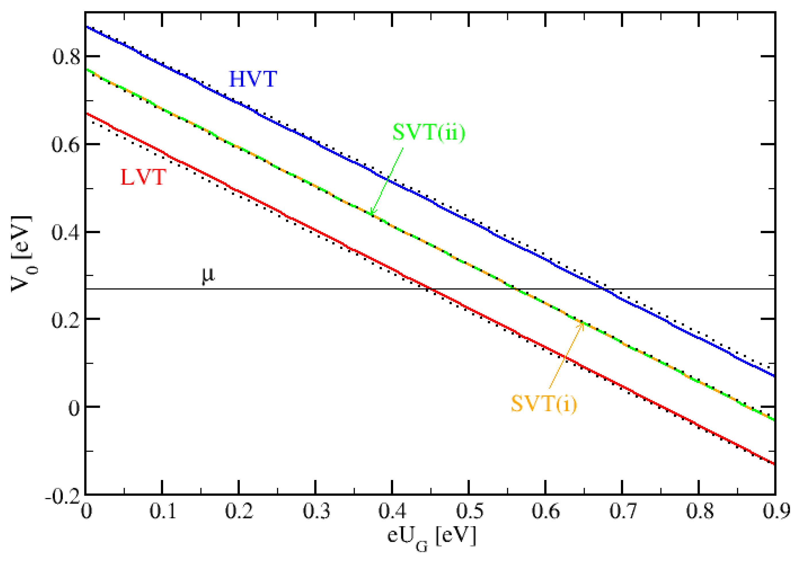
Figure 4.
For the system parameters, the barrier height from (33): n-BP with (SVT(i), orange), n-BP with (LVT, red), p-BP with (SVT(ii), green), and p-BP with (HVT, blue). In dotted black lines: Linear approximation to in Equation (36). The horizontal black solid line marks the chemical potential where the intersection points with give the threshold voltage , according to (39).

Figure 5.
For theoretical parameters the transfer characteristics for V (dashed lines) and V (solid lines). (a) for a n-BP and (b) for a p-BP. Color coding as in Figure 3. In black: Traces taken to extract the SS.
Figure 5.
For theoretical parameters the transfer characteristics for V (dashed lines) and V (solid lines). (a) for a n-BP and (b) for a p-BP. Color coding as in Figure 3. In black: Traces taken to extract the SS.


Table 1.
Electrical characteristics of multi- nMOS-transistors: above theoretical values taken from Figure 3 and Figure 5, below experimental values taken from TABLE 2 of Reference entering only experimental values as stated [18].
| Type | [mV] | [mV/dec] | ||
|---|---|---|---|---|
| LVT | 440 | 45,900 | 1474 | 70 |
| SVT(i) | 563 | 49,452 | 32 | 70 |
| SVT(ii) | 563 | 44,952 | 32 | 70 |
| HVT(i) | 686 | 39,385 | 0.7 | 70 |
| LVT | 278 | 480 | 2139 | 77 |
| SVT(i) | 429 | 332 | 16 | 76 |
| SVT(ii) | 430 | 333 | 17 | 77 |
| HVT(i) | 567 | 208 | 0.1 | 73 |
Publisher’s Note: MDPI stays neutral with regard to jurisdictional claims in published maps and institutional affiliations. |
© 2022 by the author. Licensee MDPI, Basel, Switzerland. This article is an open access article distributed under the terms and conditions of the Creative Commons Attribution (CC BY) license (https://creativecommons.org/licenses/by/4.0/).
Share and Cite
MDPI and ACS Style
Wulf, U. An Electron Waveguide Model for FDSOI Transistors. Solids 2022, 3, 203-218. https://doi.org/10.3390/solids3020014
AMA Style
Wulf U. An Electron Waveguide Model for FDSOI Transistors. Solids. 2022; 3(2):203-218. https://doi.org/10.3390/solids3020014
Chicago/Turabian StyleWulf, Ulrich. 2022. "An Electron Waveguide Model for FDSOI Transistors" Solids 3, no. 2: 203-218. https://doi.org/10.3390/solids3020014