Article

Charge Critical Phenomena in a Field Heterostructure with Two-Dimensional Crystal

by
Alexander L. Danilyuk
,
Denis A. Podryabinkin
,
Victor L. Shaposhnikov
and
Serghej L. Prischepa
*
Department of Micro- and Nanoelectronics, Belarusian State University of Informatics and Radioelectronics, 220013 Minsk, Belarus
*
Author to whom correspondence should be addressed.
Solids 2024, 5(2), 193-207; https://doi.org/10.3390/solids5020013
Submission received: 15 February 2024 / Revised: 11 March 2024 / Accepted: 3 April 2024 / Published: 6 April 2024

Abstract

:
The charge properties and regularities of mutual influence of the electro-physical parameters in a metal (M)/insulator (I)/two-dimensional crystal heterostructure were studied. In one case, the transition metal dichalcogenide (TMD) MoS2 was considered as a two-dimensional crystal, and in another the Weyl semi-metal (WSM) ZrTe5, representative of a quasi-two-dimensional crystal was chosen for this purpose. By self-consistently solving the electrostatic equations of the heterostructures under consideration and the Fermi–Dirac distribution, the relationship between such parameters as the concentration of charge carriers, chemical potential, and quantum capacitance of the TMD (WSM), as well as the capacitance of the I layer and the interface capacitance I–TMD (WSM), and their dependence on the field electrode potential, have been derived. The conditions for the emergence of charge instability and the critical phenomena caused by it are also determined.

1. Introduction

Currently, the search for and study of promising materials with new properties for solid-state information storage and processing devices is actively underway. These include both two-dimensional (2D) semi-conductors [1,2,3,4] and materials with unusual electronic states, such as topological insulators and topological semi-metals [5,6,7,8,9]. Currently, 2D semi-conductors, with a particular focus on transition metal dichalcogenides (TMDs) and heterostructures on this basis, are emerging as serious candidates for future solid-state information processing and storage device technology [10]. Their potential consists in improved device scaling and energy-efficient switching compared to traditional bulk semi-conductors, such as Si, Ge and AIII-BV compounds [2]. These materials offer significant advantages, especially in ultra-thin devices of atomic thickness. Their unique structure makes it possible to create monatomic nano-ribbons, as well as vertical and lateral heterostructures. This versatility in design, combined with their distinctive properties, paves the way to efficient energy control in electronic devices.
Considerable attention has been drawn to topological semi-metals, which can be divided into three main groups: Weyl semi-metals (WSMs), Dirac semi-metals [7,8,9] and topological semi-metals with nodal lines [11,12,13]. In Dirac and Weyl semi-metals, two doubly degenerate bands or two non-degenerate bands, respectively, intersect at singular points or nodes near the chemical potential, forming four-fold degenerate Dirac points or doubly degenerate Weyl points, and diverge linearly in all three momentum directions. These correspond to low-energy excitations. The scale of self-energy is small, which creates prospects for the development of both energy-efficient information processing elements and ultra-sensitive sensors [7,8,9]. The features of the electronic structure of the topological materials are reflected in the electronic properties and lead to a number of unusual effects, such as extremely high magneto-resistance without a tendency to saturation, high mobility and low effective mass of current carriers, non-trivial Berry phase, chiral anomaly and anomalous Hall effect, and special behavior regarding optical conductivity [8,9]. The prospects of using TMD and magnetic WSM for spin-to-charge conversion, an important effect for spintronics [14,15], is also worth noting.
Along with numerous studies of the properties of the above materials, including ab initio calculations [6,10], little attention has previously been paid to the study of their charge properties, manifested in field heterostructures. Investigation of charge phenomena in metal M (field electrode)/insulator I/semi-conductor S field heterostructures (FHS MISs) is highly relevant, since they form the root of the elemental base of modern information processing and storage devices. 2D TMDs are promising in terms of replacing traditional silicon MIS transistors in information processing devices. Weyl semi-metals are of additional interest in terms of the study of non-trivial physical effects and phenomena in FHS MISs, which can be used to create information processing devices. In FHS MIS with 2D or quasi-2D materials, issues related to the study of electro-physical parameters, such as chemical potential, charge carrier concentration, quantum capacitance, and boundary state capacitances, as well as their mutual influence on each other, are important. The inter-relationships between electro-physical parameters with the parameters of heterostructures, as well as with the potential of the field electrode, are also very relevant. The influence of various factors on the electro-physical parameters will be significantly different compared to FHS MISs based on bulk semi-conductors. Such effects will be significantly more sensitive to the properties of materials and interfaces in the TMD-based FHS MISs [16]. This contributes to the manifestation of charge instability effects, hysteresis phenomena [16,17,18,19] caused by charge localization on defect states, and phase transitions [20]. On the one hand, this will affect the stability of FHS MISs, and on the other, it will contribute to the identification of new effects that can be exploited in the development of future generations of solid-state information processing devices. As for the studies of charge instabilities in FHS MISs with WSM, there are currently no systematic studies on this issue to the best of our knowledge. However, it is worth noting that, due to the presence of low energy electronic excitations in WSMs, similar effects in WSM-based FHS MISs should be manifested with a high degree of probability.
Thus, investigation of the mutual influence of the electro-physical parameters of FHS MISs with 2D TMDs and WSMs, considering the possibility of the occurrence of charge instabilities, is relevant. In this work, for the first time, the modeling of charge properties and charge instability in the M/I/2D TMD and quasi-2D WSM field heterostructures was carried out. The simulation was performed by self–consistent solution of the electrostatic equations and the Fermi–Dirac distribution. Self-consistent solutions have been obtained that relate the electrochemical potential, the concentration of conduction electrons and TMD (WSM) quantum capacitance as a function of the field electrode potential, insulator capacitance, and spectrum of the interface trap states. The occurrence of instability of quantum capacity and the critical phenomena caused by it are predicted.

2. Charge Properties. The Model

The electron concentration ne in a 2D TMD per unit area is determined by the density of electronic states (DOSs) D(E) in the conduction band and chemical potential χ, in accordance with the Fermi–Dirac statistics [16,21]
n e χ = 0 D E f E χ d E ,
where f is the Fermi–Dirac function and D(E) follows from ab initio calculations of band energy diagrams, and χ = q U c is the chemical potential defined from the electrostatic equation (see below). Here, q is the elementary charge, and the parameter Uc represents the voltage drop across the quantum capacitance CQ [22]. The reference level for χ is the middle of the semi-conductor band gap. Currently, to calculate the charge properties and parameters of FHS MISs with 2D TMD, the following model density of electronic states of TMD is used [6,22,23]
D E = 4 π m n h 2 n Θ ( E E n ) ,
where Θ is the Heaviside function, mn is the effective mass of electrons, En is the energy of the nth sub-band (the main contribution to the concentration of charge carriers comes from the ground state with n = 0), and h is the Planck’s constant.
For the concentration of conducting electrons in WSMs, we use Equation (1) and, for the DOS, we apply a two-band model with a negative band gap, described in [24,25]
D E = 1 π 2 h 3 v F 2 c { Λ E , Δ Θ E Δ + Λ E , + Λ E , Θ E } ,
where Λ E , = E E , 2 is the energy band gap, vF is the effective Fermi velocity, and c = (1/2mn)1/2 is the parameter. The model described in [24,25] belongs to the minimum WSM model class [26]. For convenience of calculation, Equation (3) is transformed in such a way that the initially negative value Δ is assumed to be positive.
Based on the condition of electro-neutrality of FHS MISs, the relationship between the chemical potential of a 2D semi-conductor or semi-metal, the concentration of charge carriers in them, the capacitance of the insulator, and the charge at the interface states, the potential of the field electrode is determined by the electro-statics equation, which for this case is written as [27,28,29]
q U G = F m ζ s + χ + q C o x q n e χ + q n t χ ,
where UG is the potential of the field electrode, Fm is the work function of the field electrode material, ζS is the electron affinity of the TMD (WSM), qnt is the charge on trap states and Cox is the capacitance of the insulating layer.
The relation between qnt and the specific capacitance of trap states Cit has the well-known form [30,31],
C i t = d d χ q 2 n t χ
At Fm − ζS = 0 and constant density of trap states [27]
χ 1 + C i t C o x + q 2 n e ( χ ) C o x = q U G
The dependence of the charge of the trap states on the chemical potential is determined by the concentration of the occupied trap states nt and their energy spectrum. In the case of a single energy level [31]
n t χ = N t δ E E t d E 1 + g n 1 exp E χ k T = N t 1 + g n 1 exp E t χ k T ,
where Nt is the total concentration of traps, gn is the degeneracy factor of trap state, Et is the energy of trap state, k is the Boltzmann constant, T is the temperature, and δ(EEt) is the Dirac delta function. In the case of Gauss distribution of trap energies [31]
n t χ = N t d E 1 + g n 1 exp E χ k T 1 2 π 1 / 2 σ t exp E E t m 2 2 σ t 2 ,
where Etm is the energy corresponding to the maximum density of traps, and σt is the dispersion of distribution of traps energy.
The system of Equations (1)–(8) self-consistently determines the dependence of the concentration of charge carriers and χ on UG, Cox and Cit. Ultimately, it determines the self-consistent relationship of all electrical parameters of the FHS MIS with TMD or WSM. The quantum capacitance CQ, in turn, is determined by the DOS and χ according to [32].
C Q = 0 + D ( E ) d f ( E χ ) d E d E ,
In addition to quantum capacitance, important parameters are the field electrode-related capacitance CG and the TMD (WSM)-related capacitance CCH, which are also interrelated with charge carrier concentration and CQ. In the low-frequency region, the indicated capacitances are expressed as follows [27]
C G = C Q + C i t 1 + ( C Q + C i t ) / C o x
C C H = C Q 1 + ( C Q + C i t ) / C o x
The joint solution of the system of Equations (1)–(11) allows us to trace the mutual influence of the electro-physical parameters of FHS MIS with a 2D semi-conductor or semi-metal and to identify the specific features of such mutual influence under conditions of charge instability.

3. Results and Discussion

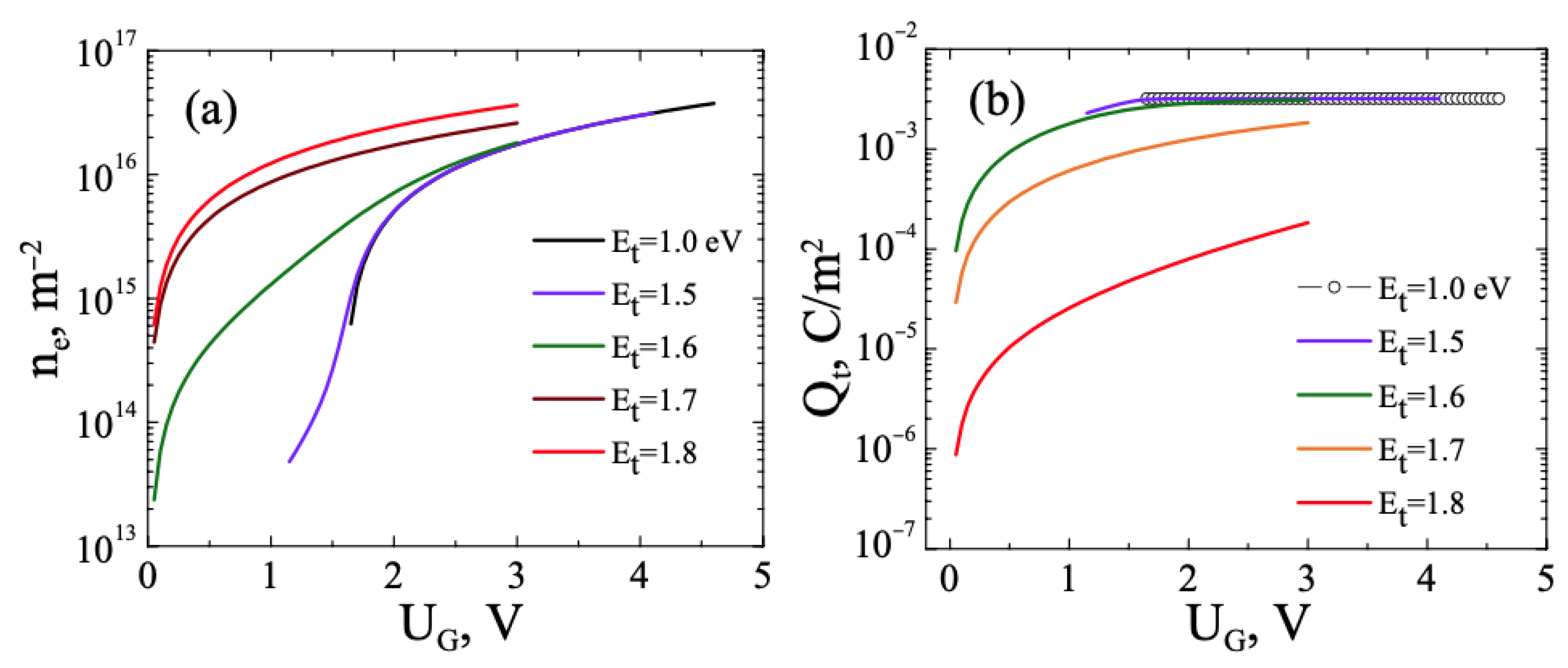
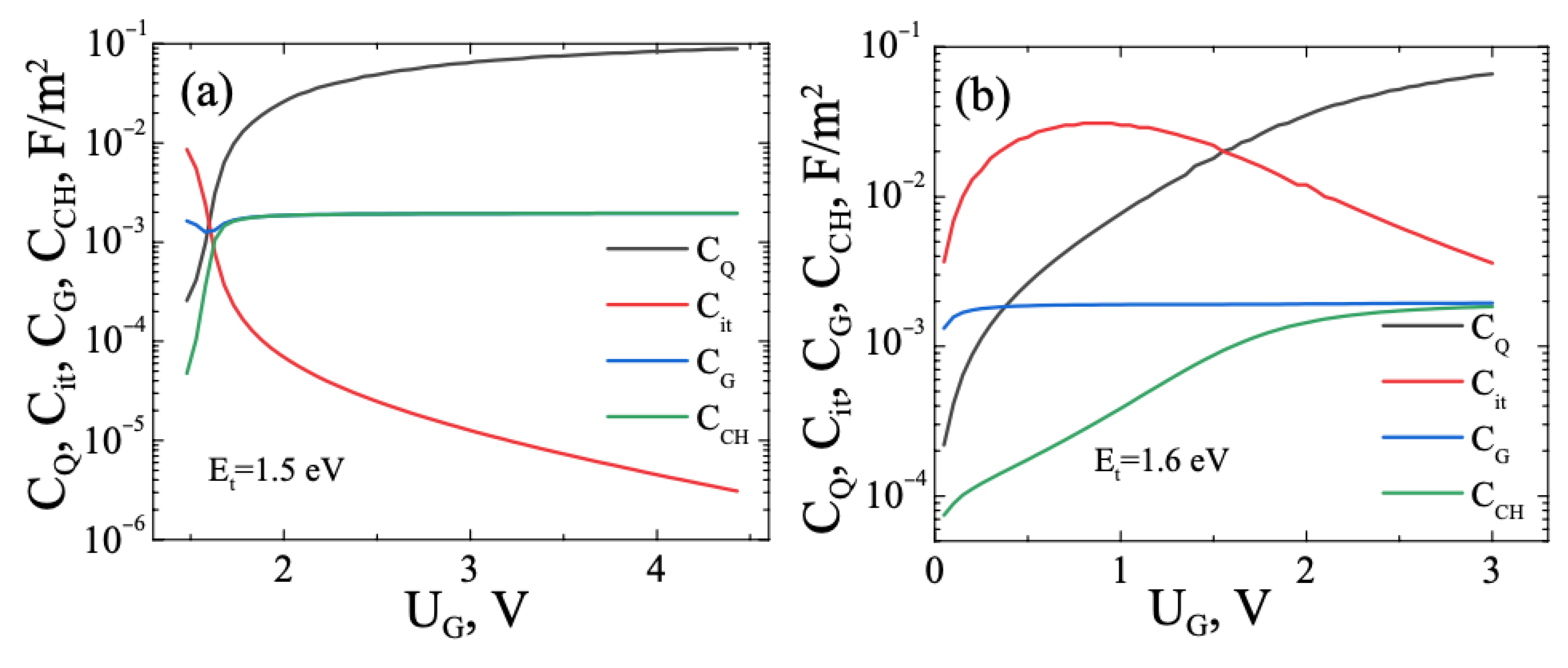
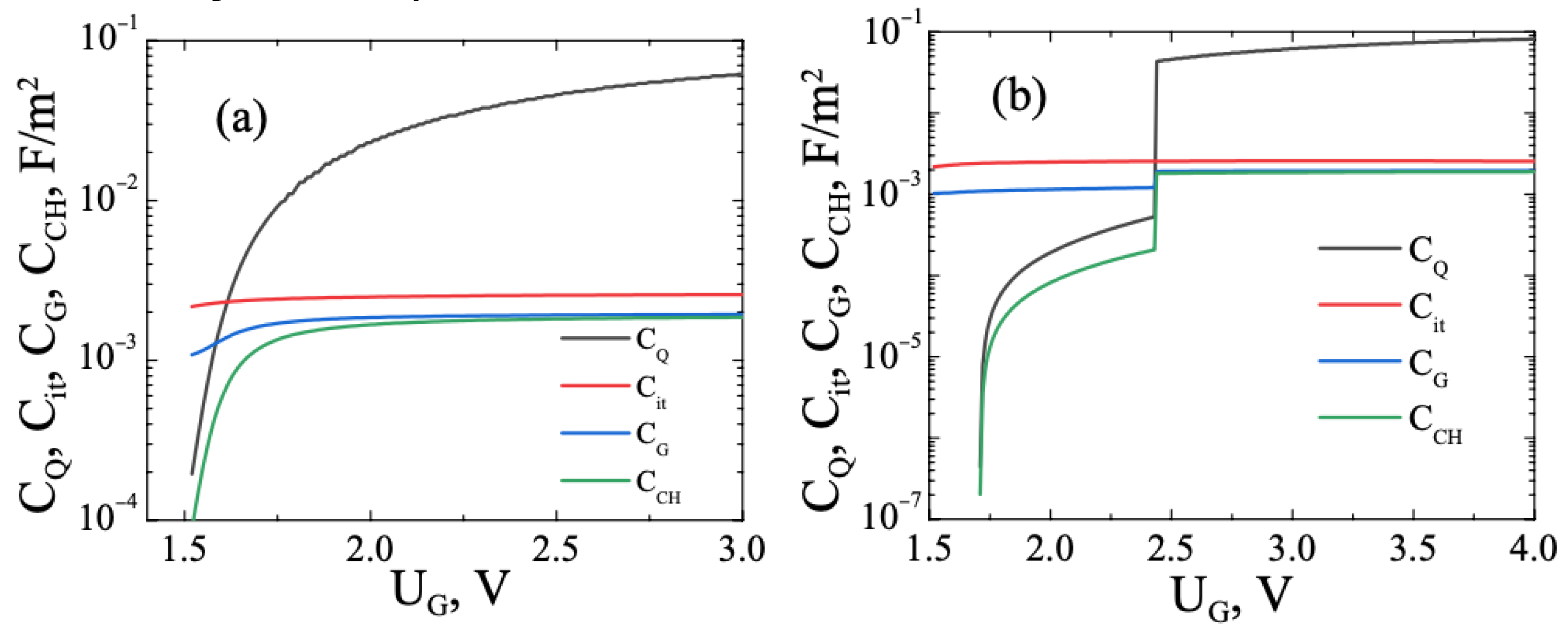
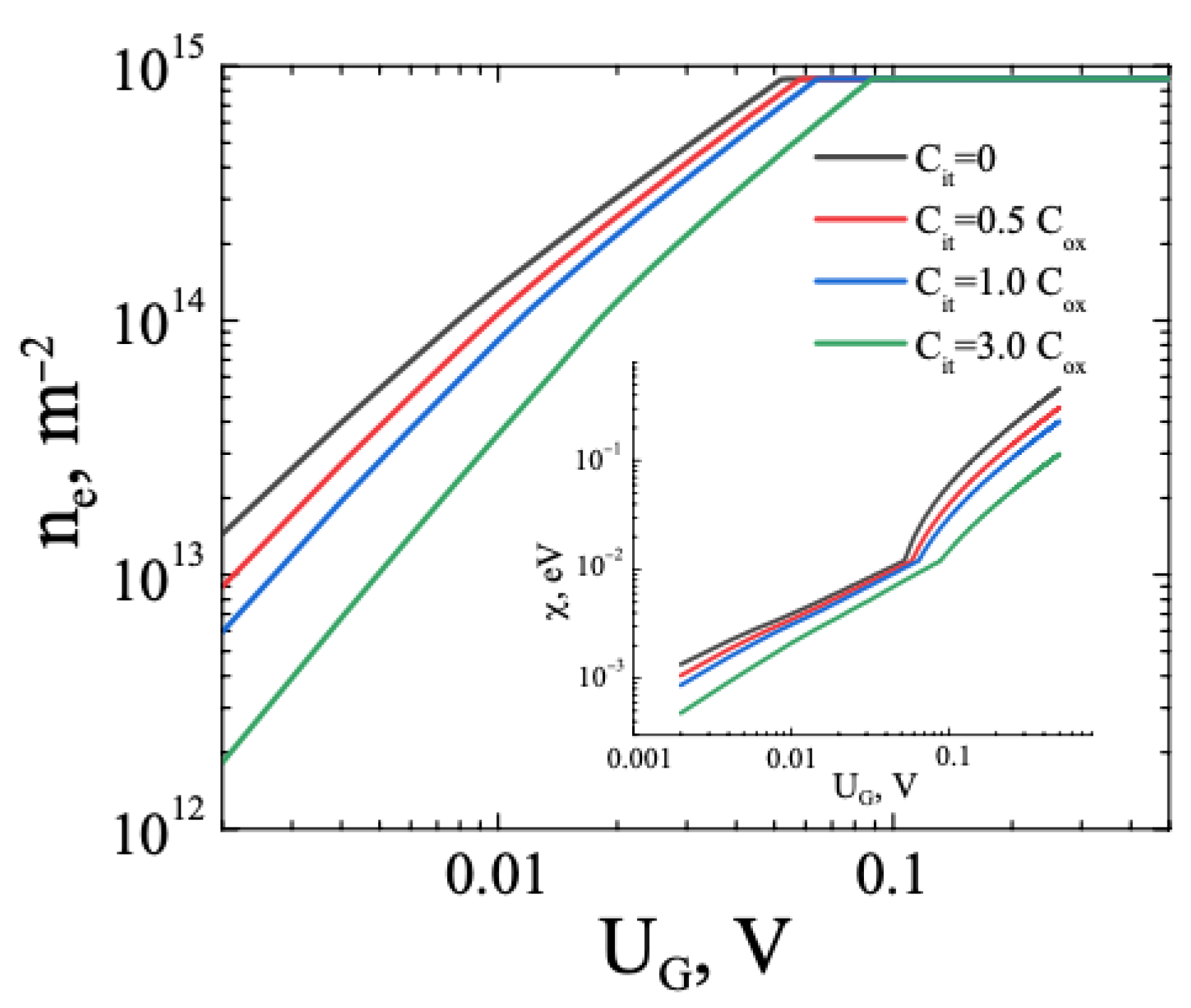
3.1. FHS MIS with TMD. Monoenergetic Traps

First, we consider the case of undoped TMD with monoenergetic traps characterized by a single energy level Et located in the TMD band gap. The energy is measured from the top of the valence band. MoS2 with a band gap of 1.86 eV is selected as TMD for calculations in this section. The total concentration of monoenergetic traps is defined as Nt. Self-consistent calculations of χ, ne, CQ, Cit, CG, CCH and electron charge on traps Qt were carried out. Calculation of the above parameters of FHS MIS were performed depending on UG and Cox = εε0/d. Here ε is the relative dielectric permittivity, ε0 is the vacuum permittivity and d is the insulating layer thickness. The Cox value was chosen as equal to 2 × 10⁻³ F/m2 (which corresponds to ε = 7, d = 30 nm), Nt = 2 × 10¹⁶ m−2, the Et varied between 1.0 and 1.8 eV and the potential UG between 0 and 5 V. Room temperature was considered, T = 300 K.
The D(E) obtained from ab initio calculations was used to evaluate the ne. For this structural optimization and electronic properties, calculations were performed employing the Vienna ab initio simulation package (VASP) [33] with the Perdew–Burke–Ernzerhof (PBE) exchange-correlation function [34]. A hybrid functional in the Heyd–Ernzerhof (HSE06) form was used to obtain more accurate band gaps [35]. The obtained DOS of the atomic monolayer MoS2, calculated with the approach developed in [33,34,35], is shown in the inset to Figure 1.
The results of self-consistent calculations revealed the following. Figure 1 shows the χ(UG) dependences at different states of Et. As can be seen at Et ≤ 1.5 eV, to achieve a self-consistent solution for the chemical potential of TMD in FHS MIS, the UG value must be at least 1.1–1.6 V. Therefore, at Et ≤ 1.5 eV and for UG < 1.1 V, there is no possibility of achieving any stable charge state of FHS MIS. The reason is an imbalance of local charges arising in the HS MIS, which does not allow achievement of the condition of electrical neutrality. This is since, to obtain the concentration of conduction electrons in MoS2, the chemical potential must be no lower than the middle of the band gap. Stable self-consistent solutions in this case exist at UG > 1.1–1.6 V, when χ exceeds a certain critical or threshold value (1.53 eV at Et = 1.0 eV and 1.6 eV at Et = 1.5 eV). Here, the chemical potential increases non-linearly and monotonically, reaching the value of 1.75 eV with an increase in UG to 4.0–4.5 V.
With increasing energy of the monoenergetic trap, starting from Et = 1.6 eV, self-consistent solutions for χ appear already from almost zero UG. As can be seen from Figure 1, there is an increase in χ at Et = 1.6 eV and 1.65 eV. Its values increase monotonically with increasing UG, approaching the values of χ for Et = 1.0 and 1.5 eV. At Et ≥ 1.75 eV, the χ values increase, and their maximum is achieved at lower UG with respect to the case of smaller Et. Further increase in the Et (up to 1.8 eV) does not cause an increase in χ.
The latter is associated with the approaching saturation of ne, as follows from Figure 2a, where the dependences ne versus UG are shown. They are qualitatively similar to the dependences of χ versus UG and are characterized by an upward shift in UG at Et ≤ 1.5 eV.
Figure 2b shows the Qt(UG) dependences. In contrast to the charge created by conduction electrons, the charge localized on traps decreases with increasing trap energy, which is associated with the degree of occupation of trap states, which decreases when the trap is shallow relative to the bottom of the conduction band.
Figure 3a,b show the results of calculations of the dependences of the CQ, CG and CCH on UG at two different values of Et (1.5 eV, Figure 3a and 1.6 eV, Figure 3b). The CQ(UG) dependences are monotonic for both values of Et. An increase in CQ is observed with increasing UG in accordance with the increase in ne (see Figure 2a). The range of CQ is 3–4 orders of magnitude.
At Et = 1.0 eV, the capacitance of the interface states that Cit sharply decreases, because the charge localized on the traps Qt ceases to depend on potential UG (see Figure 2b). In this case, as follows from Equations (10) and (11), the capacitance of the interface states does not affect the capacitances CG and CCH, which are now determined only by CQ and Cox.
As Et approaches a value of 1.5 eV, Cit begins to influence the CG and CCH capacitances. From Figure 3a, it follows that, at Et = 1.5 eV, the Cit affects CG and CCH only in the region UG = 1.5–1.7 V. In this region, we can assume that the charge system is not stable due to significant fluctuations in capacitances with a slight change in UG. At Et = 1.6 eV, Cit increases significantly, becomes comparable to CQ, and its dependence on UG becomes non-monotonic with a maximum at UG = 0.5–1.0 V (Figure 3b). This result is explained by the fact that the trap energy becomes comparable to the chemical potential. Therefore, at χEt, there is an increase in Cit with an increase in UG. We also demonstrated that, at Et > 1.7 eV, there is a sharp decline in Cit.
Thus, in the presence of electronic trap states with a monoenergetic level, their influence on the stability of the charge state of FHS MIS is determined by the relationship between the chemical potential and the energy of the traps. For the case of relatively deep traps with an energy of 1.0–1.5 eV, unstable charge states arise in the UG range up to a certain threshold value. This is because there are no conditions for the emergence of a charge balance, determined by the electrical neutrality condition of FHS MIS and the Fermi–Dirac statistics, which determine the ne(χ) dependence. The χ value in turn is determined by UG, Cox and Qt. Such an imbalance does not allow self-consistency of the chemical potential, the concentration of conduction electrons, the charge on the traps, and the charge created by the field electrode. With increasing Et, when the energy of traps becomes comparable to the value of χ, non-linear charge effects arise, which also lead to instability of charge properties in the UG range up to 2 V. This is due to an increase in the Cit which, in turn, is caused by the charge localized on the traps.
Finally, we should stress that the results obtained in this section for FHS MIS with MoS2 as TMD are qualitatively valid for other TMDs, such as, e.g., MoSe2, MoTe2, WS2, WSe2 and WTe2.

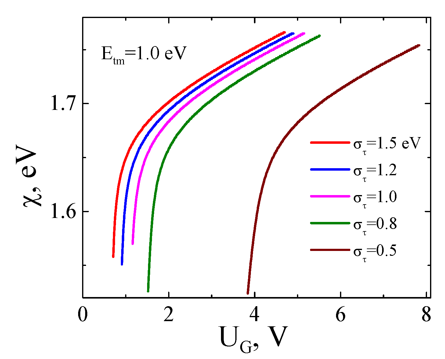
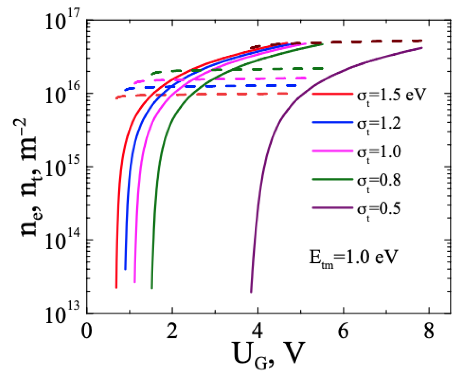
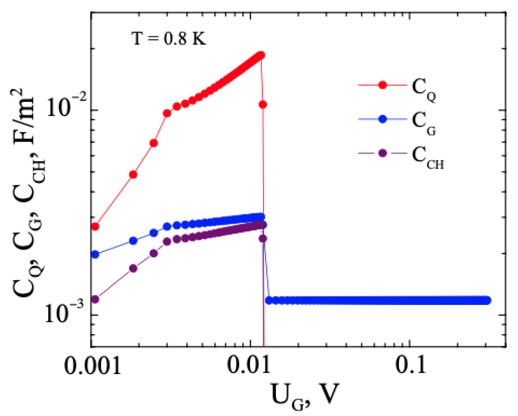
3.2. FHS MIS with TMD. Gauss Distribution for Trap Energies at the TMD–I Interface

In this section we consider the spectrum of trap states at the TMD–I interface, assuming that the energy of the states is distributed according to the Gaussian law (Equation (8)). Calculations of χ, ne, nt, CQ, CG, CCH were carried out for traps in molybdenum sulfite with the following parameters: T = 300 K, Etm = 0.8–1.2 eV, σt = 0.5–1.5 eV, Nt = 2 × 10¹⁶ m−2.
Figure 4 shows the χ(UG) and Figure 5 the dependences of ne and nt on UG at Etm = 1.0 eV. In this case, self-consistent solutions for χ and ne exist within a certain range of UG. They arise only when UG is greater than a threshold value UGth. Thus, at σt = 0.8–1.5 eV, UGth is 0.7–1.53 V, and at σt = 0.5 eV, the UGth shift reaches 4 V. Below these thresholds, there is no self-consistent solution and thus charge balance is not achieved. Therefore, we can consider the range UGUGth to be a range of charge instability. A decrease in σt shifts χ and ne towards higher UG values. A decrease in Etm, on the contrary, shifts these quantities towards lower UG.
The values of χ are in the range 1.5–1.8 eV, and the range of ne is 1013–5 × 10¹⁶ m−2. The latter can be considered as a saturation value for ne. In addition, a sharp rise occurs in the region of 0.5–2.0 V (at σt = 0.8–1.5 eV), followed by a smoother transition to saturation. The concentration of electrons localized in traps changes slightly with increasing UG; it increases with a decrease in σt at a constant value of Etm, from 0.9 × 10¹⁶ to 2 × 10¹⁶ m−2.
Figure 6a,b show the dependences of CQ, CG and CCH on UG. The results of Figure 6a were obtained for the following set of the model parameters: σt = 0.8 eV, Etm = 1.0 eV, Cox = 2 × 10⁻³ F/m2. In Figure 6b, these parameters were slightly changed, namely, σt = 0.75 eV, Etm = 1.05 eV, Cox = 3.54 × 10⁻³ F/m2. Two types of behavior of CQ versus UG have been identified: monotonic change and abrupt change. The first type is observed in the region UG = 1.5–2.0 V and is associated with the presence of an exponential change in CQ, leading to modulation of capacitances CG and CCH (Figure 6a). At the same time, the capacitance Cit does not practically change with increasing UG. However, its contribution significantly affects the change in CG and CCH in the range UG = 1.5–2.0 V. For these UG values, the change in CG and CCH reaches several times, which indirectly confirms the presence of charge instability.
Our calculation also revealed that, for larger values of σt = 1.5 eV, the value of Cit does not exceed 10−3 F/m2 and the capacitances CG and CCH are determined only by CQ. Moreover, they are close in value to each other in the entire UG range. This is due to a decrease in concentration nt at σt = 1.5 eV (see Figure 5).
The second type of dependence is shown in Figure 6b. Slight variation in the parameters of the model leads, at UG = 2.43 V, to the appearance of two roots for CQ in solving the system of Equations (1), (4), (5), (8) and (9). This causes a jump-like dependence of CQ at UG = 2.43 V, and the value of CQ changes by almost two orders of magnitude (from 5.1 × 10⁻⁴ to 0.044 F/m2). The capacitance CQ also shifts towards larger UG at small values below 10−3 F/m2 and then, due to a jump, its value is restored, reaching a value with exponential growth, compared with Figure 6a. A reverse calculation of the electron concentration based on the jump-like dependence CQ(χ) showed that a similar jump occurs for the dependence ne(χ) (see inset to Figure 6b). This also confirms the conclusion regarding the instability of the charge in FHS MIS with MoS2 at some critical relationships of its electro-physical parameters.
Note that, in the case of Gaussian distribution, in contrast to the monoenergetic traps, when instability arises due to a decrease in Et, the presence of a broadening of the energy spectrum of trap states leads practically to insensitivity of the capacitance Cit to the growth of UG, remaining almost constant under the conditions considered. This leads to the fact that the capacitances CG and CCH are determined mainly by the behavior of CQ. The situation becomes different when an abrupt change in CQ and, accordingly, in the electron concentration occurs. If, in the previous cases, a self-consistent solution was absent at certain values of UG and this was associated with the presence of instability, then here the manifestation of instability may mean that the relationships and mutual influence of the electro-physical parameters of FHS MIS are characterized by the presence of bi-stable states. This bi-stability characterizes the insulator–semi-conductor transition. Its mechanism is associated, in our opinion, with the influence of charge fluctuations leading to a transition between two states of a bi-stable system at a critical (threshold) value of UG. An increase in charge fluctuations at a critical value of UG in this case leads to a switching of states of the bi-stable system by analogy with the phenomenon of noise-induced stochastic resonance [36].
The results obtained for two types of trap states described in Section 3.1 and Section 3.2 in the general case can be explained as follows. Self-consistent solutions for χ and ne arise at certain threshold values of UG, when a charge balance in the heterostructure determined by the Fermi–Dirac statistics and the electrical neutrality condition considering the charge on trap states is achieved. For UG = 0 V, when there is no positive charge created by the field electrode potential, the chemical potential is in the middle of the band gap. In this case, in the presence of traps that capture only electrons, charge balance is not achieved, since the presence of a positive charge created by the field electrode is necessary. Physically, this is because an increase in the charge on traps leads to a mismatch between the electrical neutrality condition and the Fermi–Dirac statistics at a certain value of the potential UG, due to the absence of an increase in the DOS with energy. This is why charge imbalance arises. Self-consistency is reached only with a certain increase in χ above the energy of the middle of the band gap due to the action of the field electrode charge. This threshold effect is similar to the insulator–semi-conductor transition. Such transitions belong to the critical phenomena. They occur at critical values of some parameters of FHS MISs with TMD. In other words, we can assume the existence of critical points at which the charge balance is disrupted and the relationships between electro-physical parameters undergo qualitative changes.

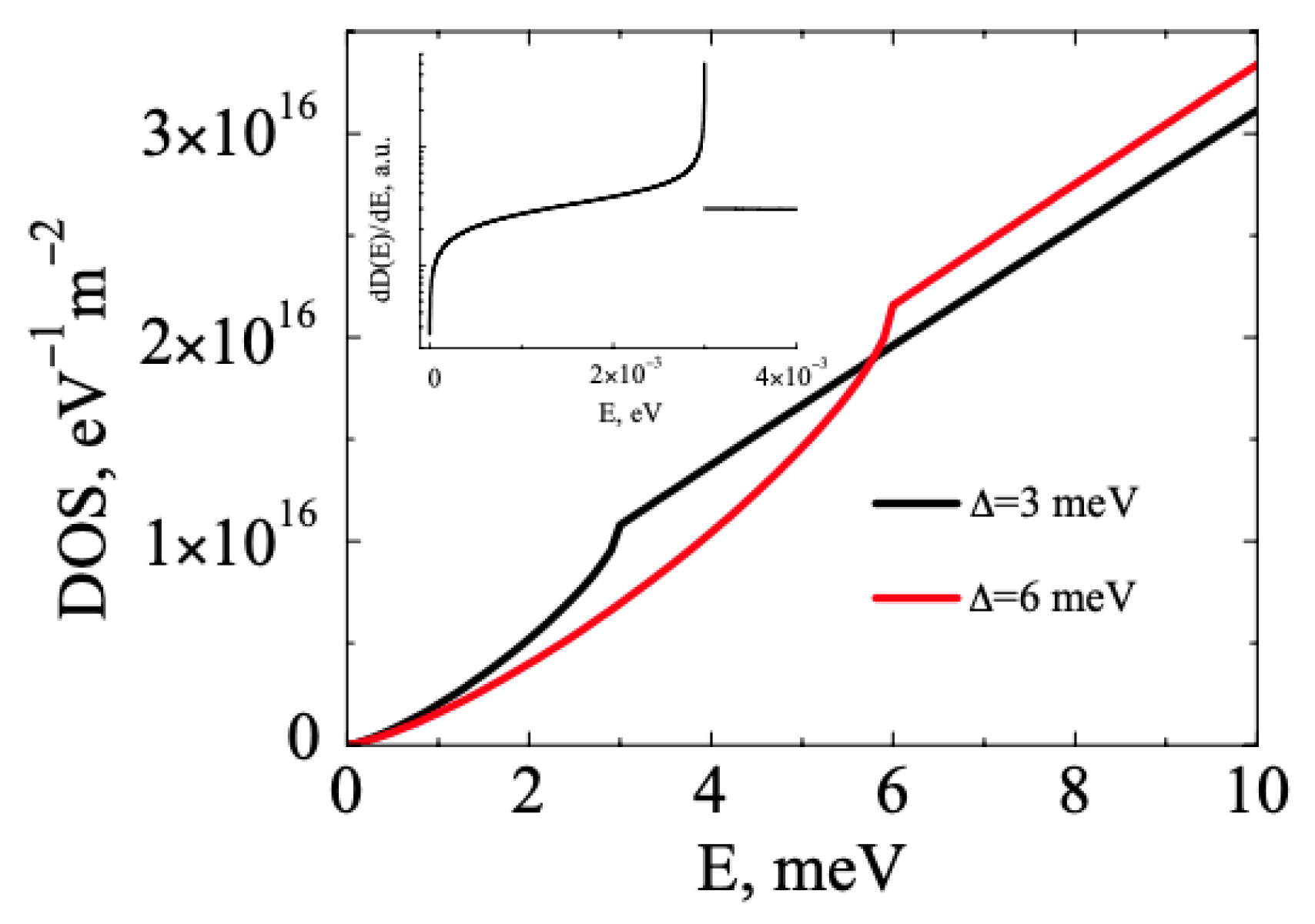
3.3. FHS MIS with WSM

Weyl semi-metals are materials in which the valence band and conduction band intersect at separate points called Weyl nodes, causing a negative band gap. When the Fermi energy is near these nodes, the electrons effectively behave as relativistic Weyl fermions with linear energy dispersion and well-defined chirality. At present, a sufficient number of materials related to WSM is already known. It is worth mentioning that these include TaAs, NbAs, TaP, NbP, WTe2, MoTe2 [6,7,37,38,39], a magnetic WSM SrRuO3 [40,41,42], etc. In this work, we chose ZrTe5, which is considered as a WSM [24,25,37]. Like many other topological semi-metals, ZrTe5 possesses small intrinsic energy scales.
The case of low temperature due to the presence of low-energy excitations in the WSM is discussed. In the region of high temperatures, the features are leveled out by thermal fluctuations. Anisotropic ZrTe5 material with an orthorhombic Cmcm phase of ZrTe5, characterized by a parabolic dispersion around the 2Δ band gap, which transforms into a linear dispersion at higher energies, corresponds to the a–c plane. The dispersion along the b direction remains parabolic at all energies. Free electron-like behavior is assumed in the b direction. In addition, ZrTe5 is characterized by the following parameters: vF = 4.9 × 10⁵ m/s, Δ = 3 meV, mn = mb = (1.8–2.0) m0 [24,25]. This semi-metal is also characterized by high mobility (1–4.5) × 105 cm2/V·s at low temperature, and effective masses in various directions are ma = Δ/va2 = 0.001 m0, mc = Δ/vc2 = 0.0025 m0. Here, m0 is the mass of a free electron, the masses ma, mc and velocities va, vc correspond to directions in the a-c planes, and the mass mb corresponds to the direction along the b axis.
For FHS MIS with ZrTe5, the case of distribution of trap states with a constant density according to Equation (6) was considered. Then, the capacitance of interface states Cit acts as a model parameter. Its value varied in the range Cit = (0–3)Cox. In addition to those indicated above for ZrTe5, the following parameters were used for simulation: T = 0.2 K and 0.8 K, ε = 16, d = 40 nm, Cox = 3.54 × 10⁻³ F/m2, UG = 0.002–0.5 V. Note also that the calculations were carried out for quasi-2D ZrTe5.
Figure 7 shows the DOS calculated from Equation (3) for Δ = 3 and 6 meV. In this model, the WSM phase has two Weyl points in the Brillouin zone, where the energy disappears, (ka, kc, kb) = (0, 0, ±Δ1/2/ħc) and, for negative band gap, the conditions for the minimal WSM model are fulfilled [26]. As follows from Figure 7, the DOS are monotonic and are characterized by the presence of kinks, at which the form of the D(E) dependence changes. Calculation of the χ(UG) dependences for various values of Cit revealed that they are qualitatively similar to the DOS, i.e., are also characterized by the presence of kinks (see inset to Figure 8). The value of χ varies in the range 5 × 10⁻⁴–0.5 eV depending on the UG potential and increases with its growth. The kink point shifts towards larger UG as Cit increases.
Figure 8 shows the concentration of conduction electrons as a function of UG. As can be seen, they are characterized by an exponential rise to a threshold value UGth, after which they sharply move to saturation, at around 1015 m−2. The capacitance Cit affects the threshold value UGth. With increasing Cit, the UGth value shifts towards higher UG, similarly to the χ(UG) dependence. The saturation of ne(UG) in this case is associated with the fact that, after the break point, the DOS of the WSM depends linearly on energy. This leads, in the region of ultra-low temperatures, where the Fermi–Dirac function has a stepwise character, to the fact that, at UG > UGth, when the chemical potential exceeds the energy, linear increase in DOS is compensated. As a result, the concentration is saturated with an almost constant value. At UG < UGth, where there is an increase in ne, the DOS depends parabolically on the energy E and χ becomes comparable to E.
Figure 9 shows the results of calculations of CQ and CG at T = 0.2 K and Cit = 3.0 Cox. The calculations of CQ revealed the presence of oscillations accompanied by their compaction near UGth and a decrease in amplitude for CG to (2.9 ± 0.3) × 10−3 F/m2. Our results also revealed that oscillations of CQ are observed at any values of Cit, and their amplitude reaches 4 orders of magnitude (10−6–10−2 F/m2). As Cit increases, the frequency of oscillations along UG increases, and a compaction in oscillations is observed closer to the UGth. When the electron concentration reaches saturation, CQ drops sharply to almost zero. This affects the CG and CCH capacitances. In this case, the capacitance CG stabilizes at UG > UGth due to the prevalence of constant capacitance Cit. A decrease in the amplitude of CG oscillations is also observed at UG < UGth: up to (2 ± 1) × 10−3 F/m2 at Cit = 0.5 Cox and up to (2.13 ± 0.87) × 10−3 F/m2 at Cit = 1.0 Cox.
The occurrence of such CQ oscillations, which characterizes the presence of charge instability in the FHS MIS with WSM, can be associated with low excitation energies of the electronic system, the non-linearity of the dependence of the concentration of electrons excited by the UG field, and the presence of a dispersion transition from a parabolic behavior to a linear one, which leads to the emergence of additional relatively small kinks in the χ(UG) and ne(UG) dependences.
When the temperature increases to 0.8 K, leveling of oscillations of CQ and, accordingly, of CG and CCH is observed (Figure 10). In this case, CQ, CG, CCH versus UG values grow up to a certain threshold value of UG, after which the CQ and CCH disappear, and the CG stabilizes at Cit > 0.
Such radical change of CQ(UG) dependence with temperature ais most likely due to a change of the Fermi–Dirac distribution. In fact, the broadening of the Fermi–Dirac function, f[(Eχ)/kT], and, accordingly, its derivative with respect to energy, which determines CQ, significantly depends on T. At T = 0.2 K, the broadening is very small and approaches the δ-function, which contributes to the formation of a set of discrete, non-overlapping bursts of the derivative f[(Eχ)/kT] in energy. This peculiar spectrum of the derivative ultimately leads to CQ oscillations. With increasing temperature, the broadening of the derivative df[(Eχ)/kT]/dE increases and such bursts overlap, smoothing out the discrete spectrum, which leads to the suppression of CQ oscillations.
The obtained behaviors for FHS MIS with WSM can be associated primarily with the features of the band structure of ZrTe5, i.e., the presence of energy bands with linear and parabolic dispersion [24].
Currently, various mechanisms for instabilities in WSM have been proposed [42,43,44,45,46,47]. In the systems in which the filled valence band is in contact with the conduction band, the instability can be caused by gapless excitations around the zero-energy manifold, which are characterized by a smaller dimension compared to the spatial dimension of the system itself [43]. Instabilities induced by a magnetic field are also considered [44,45] and, in addition to the traditional Dyakonov–Shur instability for plasmons, entropy wave instability was discovered [46]. Instability of Weyl semi-metals against Coulomb interaction could also contribute [47,48].
However, in the case under consideration, within the framework of the model used, the occurrence of charge instability, in our opinion, should be associated with the influence of the following factors. The first issue is the presence of a kink at E = Δ in the DOS, caused by a change in the dispersion law. This leads to the appearance of fluctuations of CQ due to the transition from one dispersion law to another, which has a jump-like character. This fact is illustrated in the inset to Figure 7, which shows the derivative of the DOS versus the energy for Δ = 3 meV. As can be seen at E = Δ, a discontinuity of the derivative is observed, which indicates a significant increase in fluctuations when approaching the E = Δ region. This is also indicated by the derivative of the electron concentration versus the chemical potential, which is characterized by the presence of sharp rises and falls.
The second issue is that, when approaching T = 0, at which the Fermi–Dirac function tends to a stepwise form, but has not yet become so strict, the FHS MIS with ZrTe5 charge system may lose stability due to the fact that an increase in the interface capacitance leads to a mismatch between the electrical neutrality condition and the Fermi–Dirac statistics at an energy close to the χ value. This is since, near E = Δ, the dispersion law will deviate from the parabolic towards a sharper increase in the DOS with energy. Therefore, as the Cit increases, the effect of increasing the oscillation frequency occurs when approaching the threshold value of the field electrode potential, at which saturation emerges, and the quantum capacitance decreases to zero.

4. Conclusions

Simulation of the charge properties of FHS MIS with undoped monolayer MoS2 with electron traps, characterized by such electro-physical parameters as chemical potential, conduction electron concentration, quantum capacitance, the capacitance of the TMD–I interface, the capacitance of the M–TMD and capacitance of the TMD, revealed the presence of charge instability in certain ranges of the field electrode potential. Regularities of changes in these parameters depending on the potential of the field electrode have been established for monoenergetic and Gaussian energy distributions of traps at the TMD–I interface. It is shown that, in the presence of electronic trap states with a monoenergetic level, their influence on the stability of the charge state of FHS MISs with MoS2 is determined by the relationship between χ and Et. For the case of relatively deep traps with Et = 1.0–1.5 eV, unstable charge states arise, which disappear when UG > UGth. For shallow traps this threshold disappears, and an unstable charge state does not arise for all positive UG. Such behavior is associated with the dependence of Cit on UG; it decreases along with increase in UG in the case of deep traps and increases in the case of relatively shallow traps.
With the Gaussian distribution, due to the presence of broadening of the energy spectrum of trap states, Cit does not change significantly with UG in the studied range, which determines the effect on the charge properties of FHS MIS with MoS2. It has been established that, in this case, an abrupt change in CQ and ne is also possible. We explain this instability by the emergence of bi-stability in the system. This bi-stability characterizes the insulator–semi-conductor transition. Its mechanism is associated, in our opinion, with the influence of charge fluctuations leading to a transition between two states of a bi-stable system at a critical (threshold) value of the field electrode potential. An increase in charge fluctuations leads to a switching of states of a bi-stable system by analogy with the phenomenon of noise-induced stochastic resonance.
The results obtained for two types of trap states are explained by the fact that self-consistent solutions for χ and ne arise at certain threshold values of UG, when the charge balance in the heterostructure is achieved, determined by the Fermi–Dirac statistics and the electrical neutrality condition, considering the charge on the trap states. Physically, this is because an increase in the charge on traps leads to a mismatch between the electrical neutrality condition and the Fermi–Dirac statistics at a certain value of the potential UG due to the absence of an increase in the DOS with energy. As a result, a charge imbalance arises, and self-consistency is reached only at a certain growth of χ above the energy of the middle of the band gap, due to the action of the field electrode charge. This threshold effect is similar to the insulator–semi-conductor transition. Such transitions belong to critical phenomena in which the charge balance is disrupted and the relationships between electro-physical parameters undergo qualitative changes. Our results correlate qualitatively with available experimental data, which show the presence of instability and hysteresis phenomena in transistor structures based on 2D TMD [49,50,51,52,53].
For FHS MIS with ZrTe5, the case of low temperature and a uniform energy spectrum of trap states, characterized by their capacitance, was considered. The presence of kinks in the dependence of χ and ne versus UG in the range 0.05–0.09 V was revealed, arising due to a peculiarity in the DOS, which is characterized by a change in the dispersion law for electronic states from parabolic to linear. The ne is characterized by reaching saturation at the kink point. The capacitance of the trap states in this case leads to a shift in the kink point along the field electrode potential.
The regularities of the influence of the Cit on the CQ(UG) dependence have been established. It is shown that, at T = 0.2 K, oscillations of CQ are observed at any values of the capacitance of interface states, the amplitude of which reaches four orders of magnitude, as well as a sharp drop in the region where ne reaches saturation. With Cit increase, an increase in the frequency of CQ oscillations is observed. The occurrence of such oscillations is associated with the non-linearity of the ne(UG) dependence, the presence of a transition of dispersion from parabolic to linear, which leads to the occurrence of charge fluctuations against the background of low excitation energies of the electronic system. An increase in temperature to 0.8 K leads to the disappearance of CQ oscillations.
Thus, within the framework of the model used, the obtained behavior for FHS MIS with ZrTe5 is associated with the peculiarities of its band structure, namely, the presence of energy bands with transitions between linear and parabolic dispersion. The obtained charge instability is due to two reasons. The first is the presence of a break in the DOS caused by a change in the dispersion law. This leads to the appearance of charge fluctuations of CQ due to the transition from one dispersion law to another, which has a jump-like character. This is confirmed by the presence of discontinuity of the derivative of the DOS, leading to a significant increase in such fluctuations in the break region. The second issue is determined by the stepwise form of the Fermi–Dirac function, due to which an increase in the interface capacitance leads to a mismatch between the electrical neutrality condition and the Fermi–Dirac statistics at an energy close to the value of χ, since near the break in the DOS the dispersion law will deviate from the parabolic law towards a sharper increase in the DOS, which leads to a charge imbalance, accompanied by the effect of compaction of oscillations.

Author Contributions

Conceptualization, A.L.D. and S.L.P.; Methodology, D.A.P.; Software, V.L.S.; Validation, V.L.S.; Formal analysis, D.A.P.; Investigation, A.L.D.; Writing—original draft, A.L.D.; Writing—review & editing, S.L.P.; Supervision, S.L.P. All authors have read and agreed to the published version of the manuscript.

Funding

This research was partially funded by the Belarussian Republic Foundation for Basic Research, grant F23RNF-159.

Data Availability Statement

The data presented in this study are available on request from the corresponding author due to ethical reasons.

Acknowledgments

ALD and DAP acknowledge financial support from the Belarussian Republic Foundation for Basic Research (grant F23RNF-159).

Conflicts of Interest

The authors declare no conflicts of interest.

References

  1. Huang, X.; Liu, C.; Zhou, P. 2D semiconductors for specific electronic applications: From device to system. npj 2D Mater. Appl. 2022, 6, 51. [Google Scholar] [CrossRef]
  2. Nandan, K.; Agarwal, A.; Bhowmick, S.; Chauhan, Y.S. Two-dimensional semiconductors based field-effect transistors: Review of major milestones and challenges. Front. Electron. Sec. Nano Microelectron. 2023, 4, 127779. [Google Scholar] [CrossRef]
  3. Liu, C.; Chen, H.; Wang, S.; Liu, O.; Jiang, Y.-G.; Zvang, D.W.; Liu, M.; Zhou, P. Two-dimensional materials for next-generation computing technologies. Nat. Nanotechnol. 2020, 15, 545–557. [Google Scholar] [CrossRef] [PubMed]
  4. Wei, T.; Han, Z.; Zhong, X.; Xiao, Q.; Liu, T.; Xiang, D. Two dimensional semiconducting materials for ultimately scaled transistors. iScience 2022, 25, 105160. [Google Scholar] [CrossRef]
  5. Vergniory, M.G.; Elcoro, L.; Felser, C.; Regnault, N.; Bernevig, B.A.; Wang, Z. A complete catalogue of high-quality topological materials. Nature 2019, 566, 480–485. [Google Scholar] [CrossRef] [PubMed]
  6. Naher, M.I.; Naqib, S.H. An ab-initio study on structural, elastic, electronic, bonding, thermal, and optical properties of topological Weyl semimetal TaX (X = P, As). Sci. Rep. 2021, 11, 5592. [Google Scholar] [CrossRef] [PubMed]
  7. Armitage, N.P.; Mele, E.J.; Vishwanath, A. Weyl and Dirac semimetals in three-dimensional solids. Rev. Mod. Phys. 2018, 90, 015001. [Google Scholar] [CrossRef]
  8. Bernevig, A.; Weng, H.; Fang, Z.; Dai, X. Recent progress in the study of topological semimetals. J. Phys. Soc. Jpn. 2018, 87, 041001. [Google Scholar] [CrossRef]
  9. Lv, B.Q.; Qian, T.; Ding, H. Experimental perspective on three-dimensional topological semimetals. Rev. Mod. Phys. 2021, 93, 025002. [Google Scholar] [CrossRef]
  10. Krivosheeva, A.V.; Shaposhnikov, V.L.; Borisenko, V.E.; Lazzari, J.-L. Heterostructures of two-dimensional transition metal dichalcogenides: Formation, ab initio modelling and possible applications. Mater. Today Proc. 2022, 54 Pt 1, 73–79. [Google Scholar] [CrossRef]
  11. Yang, M.-X.; Luo, W.; Chen, W. Quantum transport in topological nodal-line semimetals. Adv. Phys. X 2022, 7, 2065216. [Google Scholar] [CrossRef]
  12. Burkov, A.A.; Hook, M.D.; Balents, L. Topological nodal semimetals. Phys. Rev. B 2011, 84, 235126. [Google Scholar] [CrossRef]
  13. Bi, R.; Yan, Z.; Lu, L.; Wang, Z. Nodal-knot semimetals. Phys. Rev. B 2017, 96, 201305. [Google Scholar] [CrossRef]
  14. Han, W.; Otani, Y.; Maekawa, S. Quantum materials for spin and charge conversion. npj Quant Mater. 2018, 3, 27. [Google Scholar] [CrossRef]
  15. Zhang, S.S.L.; Burkov, A.A.; Martin, I.; Heinonen, O.G. Spin-to-Charge Conversion in Magnetic Weyl Semimetals. Phys. Rev. Lett. 2019, 123, 187201. [Google Scholar] [CrossRef] [PubMed]
  16. Makovskaya, T.I.; Danilyuk, A.L.; Krivosheeva, A.V.; Shaposhnikov, V.L.; Borisenko, V.E. Charge properties of the MOS transistor structure with the channel made from a two–dimensional crystal. Russ. Microelectron. 2020, 49, 507–515. [Google Scholar] [CrossRef]
  17. Kaushik, N.; Mackenzie, D.M.A.; Thakar, K.; Goyal, N.; Mukherjee, B.; Boggild, P.; Petersen, D.H.; Lodha, S. Reversible hysteresis inversion in MoS2 field effect transistors. npj 2D Mater. Appl. 2017, 1, 34. [Google Scholar] [CrossRef]
  18. Late, D.J.; Liu, B.; Matte, H.S.S.R.; Dravid, V.P.; Rao, C.N. Hysteresis in single-layer MoS2 field effect transistors. ACS Nano, 2012; 6, 5635–5641. [Google Scholar] [CrossRef]
  19. Shu, J.P.; Wu, G.; Guo, Y.; Liu, B.; Wei, X.; Chen, Q. The intrinsic origin of hysteresis in MoS2 field effect transistors. Nanoscale 2016, 8, 3049–3056. [Google Scholar] [CrossRef] [PubMed]
  20. Lin, Y.-C.; Dumcenco, D.O.; Huang, Y.-S.; Suenaga, K. Atomic mechanism of the semiconducting-to-metallic phase transition in single–layered MoS2. Nat. Nanotechnol. 2014, 9, 391–396. [Google Scholar] [CrossRef] [PubMed]
  21. Das, S.; Sebastian, A.; Pop, E.; McClellan, C.J.; Franklin, A.D.; Grasser, T.; Knobloch, T.; Illarionov, Y.; Penumatcha, A.V.; Appenzeller, J.Z.; et al. Transistors based on two–dimensional materials for future integrated circuits. Nat. Electron. 2021, 4, 786–799. [Google Scholar] [CrossRef]
  22. Jiménez, D. Drift-diffusion model for single layer transition metal dichalcogenide field-effect transistors. Appl. Phys. Lett. 2012, 101, 243501. [Google Scholar] [CrossRef]
  23. Cao, W.; Kang, J.; Liu, W.; Banerjee, K. A Compact Current-Voltage Model for 2D Semiconductor Based Field-Effect Transistors Considering Interface Traps, Mobility Degradation, and Inefficient Doping Effect. IEEE Trans. Electron Devices 2014, 61, 4282–4290. [Google Scholar] [CrossRef]
  24. Martino, E.; Crassee, I.; Eguchi, G.; Santos-Cottin, D.; Zhong, R.D.; Gu, G.D.; Berger, H.; Rukelj, Z.; Orlita, M.; Homes, C.C.; et al. Two-Dimensional Conical Dispersion in ZrTe5 Evidenced by Optical Spectroscopy. Phys. Rev. Lett. 2019, 122, 217402. [Google Scholar] [CrossRef] [PubMed]
  25. Rukelj, Z.; Homes, C.C.; Orlita, M.; Akrap, A. Distinguishing the gapped and Weyl semimetal scenario in ZrTe5: Insights from an effective two-band model. Phys. Rev. B 2020, 102, 125201. [Google Scholar] [CrossRef]
  26. McCormick, T.M.; Kimchi, I.; Trivedi, N. Minimal models for topological Weyl semimetals. Phys. Rev. B 2017, 95, 075133. [Google Scholar] [CrossRef]
  27. Zebrev, G.I. Graphene Field Effect Transistors: Diffusion-Drift Theory. In Physics and Applications of Graphene—Theory; Mikhailov, S., Ed.; IntechOpen, Rijeka, Croatia, 2011; Chapter 23, pp. 475–498. [CrossRef]
  28. Marin, E.G.; Bader, S.J.; Jena, D. A New Holistic Model of 2-D Semiconductor FETs. IEEE Trans. Electron Devices 2018, 65, 1239–1245. [Google Scholar] [CrossRef]
  29. Najam, F.; Tan, M.L.P.; Ismail, R.; Yu, Y.S. Two-dimensional (2D) transition metal dichalcogenide semiconductor field-effect transistors: The interface trap density extraction and compact model. Semicond. Sci. Technol. 2015, 30, 075010. [Google Scholar] [CrossRef]
  30. Sze, S.M.; Ng, K.K. Physics of Semiconductor Devices, 3rd ed.; John Wiley & Sons, Inc.: Hoboken, NJ, USA, 2008; 826p. [Google Scholar]
  31. Kao, K.-C.; Hwang, W. Electrical Transport in Solids with Particular Reference to Organic Semiconductors; Pergamon Press: Oxford, UK, 1981; 663p. [Google Scholar]
  32. Luryi, S. Quantum Capacitance Devices. Appl. Phys. Lett. 1988, 52, 501–503. [Google Scholar] [CrossRef]
  33. Kresse, G.; Furthmüller, J. Efficient iterative schemes for ab initio total-energy calculations using a plane-wave basis set. Phys. Rev. B 1996, 54, 11169. [Google Scholar] [CrossRef] [PubMed]
  34. Perdew, J.P.; Burke, K.; Ernzerhof, M. Generalized gradient approximation made simple. Phys. Rev. Lett. 1996, 77, 3865–3868, Erratum in Phys. Rev. Lett. 1997, 78, 1396. [Google Scholar] [CrossRef] [PubMed]
  35. Heyd, J.; Scuseria, G.E.; Ernzerhof, M. Hybrid functionals based on a screened Coulomb potential. J. Chem. Phys. 2003, 118, 8207–8215. [Google Scholar] [CrossRef]
  36. Anishchenko, V.S.; Neiman, A.B.; Moss, F.; Shimansky-Geier, L. Stochastic resonance: Noise-enhanced order. Physics-Uspekhi 1999, 42, 7–36. [Google Scholar] [CrossRef]
  37. Liang, T.; Lin, J.; Gibson, Q.; Kushwaha, S.; Liu, M.; Wang, W.; Xiong, H.; Sobota, J.A.; Hashimoto, M.; Kirchmann, P.S.; et al. Anomalous Hall effect in ZrTe5. Nat. Phys. 2018, 14, 451–455. [Google Scholar] [CrossRef]
  38. Zheng, H.; Hasan, M.Z. Quasiparticle interference on type-I and type-II Weyl semimetal surfaces: A review. Adv. Phys. X 2018, 3, 1466661. [Google Scholar] [CrossRef]
  39. Sun, Y.; Wu, S.-C.; Ali, M.N.; Felser, C.; Yan, B. Prediction of Weyl semimetal in orthorhombic MoTe2. Phys. Rev. B 2015, 92, 161107. [Google Scholar] [CrossRef]
  40. Takiguchi, K.; Wakabayashi, Y.K.; Irie, H.; Krockenberger, Y.; Otsuka, T.; Sawada, H.; Nikolaev, S.A.; Das, H.; Tanaka, M.; Taniyasu, Y.; et al. Quantum transport evidence of Weyl fermions in an epitaxial ferromagnetic oxide. Nat. Commun. 2020, 11, 4969. [Google Scholar] [CrossRef] [PubMed]
  41. Lin, W.; Liu, L.; Liu, Q.; Li, L.; Shu, X.; Li, C.; Xie, Q.; Jiang, P.; Zheng, X.; Guo, R.; et al. Electric Field Control of the Magnetic Weyl Fermion in an Epitaxial SrRuO3 (111) Thin Film. Adv. Mater. 2021, 33, 2101316. [Google Scholar] [CrossRef] [PubMed]
  42. Toyoda, S.; Yamada, R.; Kaneko, Y.; Tokura, Y.; Ogawa, N. Weyl fermions in SrRuO3 detected by Brillouin light scattering. Appl. Phys. Lett. 2022, 120, 242408. [Google Scholar] [CrossRef]
  43. Sur, S.; Nandkishore, R. Instabilities of Weyl loop semimetals. New J. Phys. 2016, 18, 115006. [Google Scholar] [CrossRef]
  44. Amitani, T.; Nishida, Y. Dynamical chiral magnetic current and instability in Weyl semimetals. Phys. Rev. B 2023, 107, 014302. [Google Scholar] [CrossRef]
  45. Yadav, N.; Deo, N. Magnetotransport in Weyl semimetal with and without disorder and the effect of tilted magnetic field. Phys. E Low-Dimens. Syst. Nanostruct. 2023, 148, 115601. [Google Scholar] [CrossRef]
  46. Sukhachov, P.O.; Gorbar, E.V.; Shovkovy, I.A. Entropy Wave Instability in Dirac and Weyl Semimetals. Phys. Rev. Lett. 2021, 127, 176602. [Google Scholar] [CrossRef] [PubMed]
  47. Xue, F.; Zhang, X.-X. Instability and topological robustness of Weyl semimetals against Coulomb interaction. Phys. Rev. B 2017, 96, 195160. [Google Scholar] [CrossRef]
  48. Boettcher, I. Interplay of Topology and Electron-Electron Interactions in Rarita-Schwinger-Weyl semimetals. Phys. Rev. Lett. 2020, 124, 127602. [Google Scholar] [CrossRef] [PubMed]
  49. Li, T.; Du, G.; Zhang, B.; Zeng, Z. Scaling behavior of hysteresis in multilayer MoS2 field effect transistors. Appl. Phys. Lett. 2014, 105, 093107. [Google Scholar]
  50. Park, Y.; Baac, H.W.; Heo, J.; Yoo, G. Thermally activated trap charges responsible for hysteresis in multilayer MoS2 field-effect transistors. Appl. Phys. Lett. 2016, 108, 083102. [Google Scholar] [CrossRef]
  51. Illarionov, Y.Y.; Rzepa, G.; Waltl, M.; Knobloch, T.; Grill, A.; Furchi, M.M.; Mueller, T.; Grasser, T. The role of charge trapping in MoS2/SiO2 and MoS2/hBN field-effect transistors. 2D Mater. 2016, 3, 035004. [Google Scholar] [CrossRef]
  52. Illarionov, Y.Y.; Knobloch, T.; Waltl, M.; Rzepa, G.; Pospischil, A.; Polyushkin, D.A.; Furchi, M.M.; Mueller, T.; Grasser, T. Energetic mapping of oxide traps in doublegated MoS2 field-effect transistors. 2D Mater. 2017, 4, 025108. [Google Scholar] [CrossRef]
  53. Knobloch, T.; Rzepa, G.; Illarionov, Y.Y.; Waltl, M.; Schanovsky, F.; Stampfer, B.; Furchi, M.; Mueller, T.; Grasser, T. A Physical Model for the Hysteresis in MoS2 Transistors. J. Electr. Dev. Soc. 2018, 6, 972–978. [Google Scholar] [CrossRef]
Figure 1. Chemical potential χ of MoS2 versus UG of FHS MIS at different energy levels Et of monoenergetic traps. Inset: DOS of the atomic monolayer MoS2.
Solids 05 00013 g001
Figure 2. (a) Density of conduction electrons ne versus UG of FHS MIS at different energy levels Et of monoenergetic traps; (b) electron charge on traps Qt versus UG of FHS MIS at different energy levels of Et of monoenergetic traps.
Solids 05 00013 g002
Figure 3. Quantum capacitance CQ, capacitance of the I–TMD interface Cit, field electrode–TMD capacitance CG and TMD capacitance CCH versus UG of FHS MIS at (a) Et = 1.5 eV and (b) Et = 1.6 eV.
Solids 05 00013 g003
Figure 4. Chemical potential χ of MoS2 versus UG of FHS MIS at different dispersion σt of Gauss distribution of traps energy.
Solids 05 00013 g004
Figure 5. Density of conduction electrons ne (solid lines) and density of electrons localized in traps nt (dashed lines) versus UG of FHS MIS at different dispersion σt of Gauss distribution of traps energy.
Solids 05 00013 g005
Figure 6. (a,b) Quantum capacitance CQ, capacitance of the I–TMD interface Cit, field electrode–TMD capacitance CG, and TMD capacitance CCH versus UG of FHS MIS in the case of Gauss distribution of traps energy at two slightly different sets of model parameters. For details, see the text. Inset to (b): Density of conduction electrons ne versus chemical potential χ for MoS2.
Solids 05 00013 g006
Figure 7. Density of states DOS of ZrTe2 at two energy gap values. Inset: The first derivative of DOS versus energy for ZrTe5 at ∆ = 3 meV.
Solids 05 00013 g007
Figure 8. Density of conduction electrons ne versus UG of FHS MIS at different values of the capacitance of the I–WSM interface Cit. Inset: Chemical potential of ZrTe5 versus UG of FHS MIS at different values of the capacitance of the I–WSM interface Cit.
Solids 05 00013 g008
Figure 9. Quantum capacitance CQ of ZrTe5 and field electrode–WSM capacitance CG versus UG of FHS MIS. T = 0.2 K.
Solids 05 00013 g009
Figure 10. Quantum capacitance CQ of ZrTe5, field electrode–WSM capacitance CG and WSM capacitance CCH versus UG of FHS MIS. T = 0.8 K.
Solids 05 00013 g010
Disclaimer/Publisher’s Note: The statements, opinions and data contained in all publications are solely those of the individual author(s) and contributor(s) and not of MDPI and/or the editor(s). MDPI and/or the editor(s) disclaim responsibility for any injury to people or property resulting from any ideas, methods, instructions or products referred to in the content.

