Abstract
Additive manufacturing (AM) as a disruptive technique has offered great potential to design and fabricate many metallic components for aerospace, medical, nuclear, and energy applications where parts have complex geometry. However, a limited number of materials suitable for the AM process is one of the shortcomings of this technique, in particular laser AM of copper (Cu) is challenging due to its high thermal conductivity and optical reflectivity, which requires higher heat input to melt powders. Fabrication of composites using AM is also very challenging and not easily achievable using the current powder bed technologies. Here, the feasibility to fabricate pure copper and copper-carbon nanotube (Cu-CNT) composites was investigated using laser powder bed fusion additive manufacturing (LPBF-AM), and 10 × 10 × 10 mm3 cubes of Cu and Cu-CNTs were made by applying a Design of Experiment (DoE) varying three parameters: laser power, laser speed, and hatch spacing at three levels. For both Cu and Cu-CNT samples, relative density above 90% and 80% were achieved, respectively. Density measurement was carried out three times for each sample, and the error was found to be less than 0.1%. Roughness measurement was performed on a 5 mm length of the sample to obtain statistically significant results. As-built Cu showed average surface roughness (Ra) below 20 µm; however, the surface of AM Cu-CNT samples showed roughness values as large as 1 mm. Due to its porous structure, the as-built Cu showed thermal conductivity of ~108 W/m·K and electrical conductivity of ~20% IACS (International Annealed Copper Standard) at room temperature, ~70% and ~80% lower than those of conventionally fabricated bulk Cu. Thermal conductivity and electrical conductivity were ~85 W/m·K and ~10% IACS for as-built Cu-CNT composites at room temperature. As-built Cu-CNTs showed higher thermal conductivity as compared to as-built Cu at a temperature range from 373 K to 873 K. Because of their large surface area, light weight, and large energy absorbing behavior, porous Cu and Cu-CNT materials can be used in electrodes, catalysts and their carriers, capacitors, heat exchangers, and heat and impact absorption.
1. Introduction
Additive manufacturing (AM) as a layer-by-layer manufacturing technique has attracted extensive attention of researchers and has revolutionized almost every industry sector. AM has important advantages over traditional manufacturing processes, including high material utilization rate and high degrees of freedom, to fabricate complex designs with porous [1], hollow, or fine features and conformal shapes without special tooling and expensive traditional processes [2,3]. One of the shortcomings of AM is the limited number of alloys processable by this technique such as titanium (Ti), nickel (Ni), steel, and AlSi10Mg [4,5,6,7,8,9,10,11,12,13,14,15,16,17,18,19]. Ongoing research in the metals and alloys community is concentrated on expanding the number of available alloys [3].
Pure copper (Cu) has excellent mechanical, chemical, and physical properties, including high thermal and electrical conductivity, making them the potential materials for thermal management components, heat exchangers, radiators, and other electrical components [1]. However, advances made have increased the demand for lighter materials with superior electrical, thermal, and mechanical performances as an alternative to heavy Cu in automobiles and aircrafts applications to enhance energy efficiency and reduce carbon footprint [20]. Recently, copper–carbon nanotube (Cu-CNT) composites have been developed as a substitute for Cu in order to reduce the density of functional and structural materials made of Cu and to improve their mechanical, electrical, and thermal properties [20,21,22,23]. CNTs have been extensively explored for a variety of applications, such as energy storage and conversion, catalysis, and drug delivery due to many favorable attributes such as low density, excellent strength, high thermal conductivity, low thermal expansion coefficient, and good self-lubricating property [24,25]. The addition of CNTs to Cu can act as weight reducers, rendering the composites lighter in addition to transmitting their own exceptional properties to Cu in order to composites with superior performance [20]. However, the main challenge is the manufacturing of metal-CNTs due to van der Waals’ force between the CNT surfaces, which tend to form bundles [24] and cause the CNTs to agglomerate. So far, approaches to fabricate Cu-CNT include (i) powder-processing, which involves making Cu-CNTs composite powders by mixing CNT and Cu powders using ball/attrition milling or ultrasonication, followed by compaction methods such as spark plasma sintering, isostatic pressing, high-pressure torsion, and forging; (ii) electrodeposition; (iii) physical vapor deposition; and (iv) magnetron sputtering [20]. However, new methods to homogeneously mix CNTs in the Cu matrix and scaled-up fabrication are still required.
AM of pure Cu and Cu alloys has been studied using a variety of additive methods such as selective laser sintering (SLS) [26], selective laser melting (SLM) [3,27], selective electron beam melting (SEBM) [28], and binder jetting (BJ) [29]. Although there are some studies on AM of pure Cu using laser processing, it is still a challenge to produce dense and crack-free parts due to the high thermal conductivity and optical reflectivity of pure Cu on the laser in molten and liquid states [2]. The available laser AM machines use laser wavelength in the range of 1000–1100 nm. The pure Cu powder reflects 98% of the laser in this wavelength range, leading to energy loss and insufficient heat input to melt the powder; therefore, higher energy density is required [2]. By combining the ability to produce geometrically complex-shaped parts using AM and the promising properties of Cu-CNTs, components with greater performance could potentially be fabricated. However, to the best of authors’ knowledge, the laser processing of Cu-CNTs has not been reported yet.
In this paper, Cu-CNTs composites have been fabricated using h an innovative approach through multi-step manufacturing process including milling to mix the CNTs and Cu powder efficiently and uniformly, and melting and solidification of the mixture using powder bed additive manufacturing process. The density, surface roughness, electrical, and thermal conductivity measurements were made to investigate the effect of process parameters on the properties and qualities of the final parts in order to find the process window.
2. Materials and Methods
Cu powders with purity above 99.8% were obtained from Stanford Advanced Materials, Lake Forest, CA, USA. The 0.5 wt.% multi-walled carbon nanotube (MWCNTs) with purity of >98%, outer diameter of 4–6 nm, and length of 10–20 µm were prepared from Nanostructured & Amorphous Materials, Inc., Houston, TX, USA. Cu and CNTs were mixed at room temperature using Hd-01 Attritor ball milling (Union Process, Inc located in Akron, OH, USA) for 2 h, at a speed of 300 rpm, and ball (steel) to powder ratio of 5:1.
Laser powder bed additive manufacturing was then used to build Cu and Cu-CNTs cubes in the size of 10 × 10 × 10 mm3. Concept Laser Mlab machine with a maximum output power of 100 W was used for this fabrication. A systematic full factorial Design of Experiment (DoE) with 27 runs of experiments was conducted by varying 3 process parameters at 3 levels, as shown in Table 1.

Table 1.
DoE factors and levels.
The layer thickness was fixed at 0.03 mm. The laser direction changed 90° every layer. Steel was used as the base plate, and laser scanning was performed without preheating the base plate.
After the build was completed, the as-built samples were cut out. Before preparation for microstructural analysis, density and surface roughness of the samples were measured. The roughness measurement was conducted on the top surface of the as-built samples using a profilometer (Bruker Dektak XT) with a 12.5 μm diameter diamond tip stylus. The scan length and the applied stylus force were selected as 5 mm and 3 mg, respectively, and average surface roughness (Ra) was measured and reported by the software. Density of all samples was measured using Archimedes method by weighing the sample in air and deionized water at 22 °C. The air bubbles on the samples’ surfaces in water were removed before taking readings. Three readings were performed, and the average value was reported. The relative part density was calculated while considering 8.96 g/cm3 as the theoretical density for pure Cu and 8.93 g/cm3 as the density for Cu-0.5 wt.% CNT.
After density and surface roughness measurements, the samples were cut into multiple layers at different distance from the build plate, and the surfaces were then mechanically polished with silicon carbide papers and diamond polishing paste to mirror finish for further characterization. A scanning electron microscope (SEM, Focused Ion Beam/SEM-Auriga-Zeiss, White Plains, NY, USA) equipped with energy dispersive spectroscopy (EDS) was used for microstructural characterization. Imagej software (National Institute of Health, Washington, DC, USA) was used to measure porosity.
Furthermore, thermal conductivity (thermal diffusivity and heat capacity) of the samples were measured using laser-flash methods DLF1600 and DSC650 (TA instrument, New Castle, DE, USA) at temperature ranges from 298 K to 1073 K with 100 K increments. Heat capacity was measured with the three-run method, in which the first run was for empty alumina pan ramping from room temperature to the desired temperature at 20 K/min, and the second run was for the Sapphire sample, which served as a reference for the third run of the sample. Thermal conductivity (k: W/m.K) was then calculated from both thermal diffusivity (: cm2/s) and heat capacity (: J/g.K) data using the following relations [30]:
where is the density of sample in g/cm3, measured as part of the experiment.
The electrical conductivity of the samples was measured using Sigmascope SMP350 (Fisher Technology Inc., Windsor, CT, USA) at 60 kHz and room temperature (20 °C). The calibration was performed using Cu samples with electrical conductivity of 101.0% International Annealed Copper Standard (IACS). The average value calculated from 10 readings was reported.
To relate measured characteristics to the build parameters, the DoE was used to determine the effect of volumetric energy density (VED) (process parameters) on part quality. The formula for calculating VED is as follows [6]:
where ε is volumetric energy density in J/mm3, P is the laser power in W, ν is the scanning speed in mm/s, d is powder layer thickness in mm, and h is hatch spacing in mm.
3. Results
3.1. Evaluation of Powders
SEM images of the powders are shown in Figure 1. Figure 1a shows the SEM image of as-received Cu powder before the addition of the CNTs. Powder particles are mostly spherical with particle sizes in the range of 25–100 µm. The images of the Cu powders after mixing with 0.5 wt.% CNTs after ball milling at room temperature are shown in Figure 1c,d. High magnification image of one particle in Figure 1d indicated attachment of CNTs to the surface of Cu powder. CNT strands are clearly seen on the surface of the Cu particles in Figure 1d. This distribution is clearly uniform as similar dark areas are observed on all Cu particles. Simple mixing of the CNTs with Cu showed no attachment of CNTs to Cu surfaces. However, after 2 h of milling, CNTs clearly adhered to the surface of the Cu. Milling is used repeatedly in the literature to mix CNTs with other metals [20]. In addition to SEM imaging, EDS elemental mapping was conducted to evaluate the elements on the surface of the Cu. EDS showed carbon element accumulation on the surface of Cu particle, as shown in Figure 2, indicating that CNTs indeed mixed with Cu particles. During ball-milling, the local generation of the high pressure due to the collision between the rigid balls allows for detangling and successful dispersion of CNTs in between Cu particles [31].
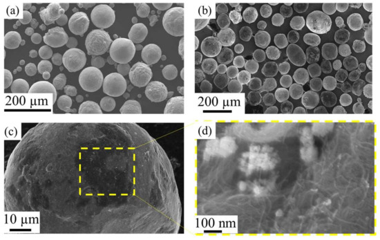
Figure 1.
Scanning electron microscopy of (a) Cu powder, (b) Cu-CNTs powders, (c) high magnification of one Cu particle after mixing with CNTs, and (d) high magnification of dark parts (selected dashed square) showing CNTs on surface of Cu.
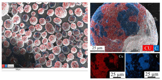
Figure 2.
Energy dispersive spectroscopy (EDS) mapping of Cu particle after mixing with CNTs confirming attachment of CNTs on surface of Cu.
3.2. Relative Density and Surface Roughness of As-Built Parts
Figure 3a,b show images of the as-built Cu and Cu-CNTs at all 27 runs of experiment, respectively, indicating that both samples can successfully be fabricated using LPBF-AM. The numbers on the top of each sample represent the number of experiments. The AM samples with the addition of CNTs showed relatively higher surface roughness and more porous structure than the as-fabricated pure Cu. Density and surface roughness are the essential attributes for evaluating the print quality in order to optimize process parameters. Figure 4a shows the roughness and relative density calculated for Cu samples with their corresponding process parameters. The relative density of as-built Cu-CNT samples is shown in Figure 4b along with their process parameters. AM Cu-CNTs have a very rough surface (~1 mm), which was beyond the limitation of the measurement equipment and not included in the figure. However, a close-up image of the surface is provided as insets in Figure 3 to show relative surface differences. As seen in this figure, a Cu sample with relative density more than ~94% was successfully fabricated using LPBF-AM at lowest hatch spacing of 90 μm, power of 93 W, and speed of 47 mm/s. The highest density achieved for Cu-CNT samples was about 81%. This was achieved at hatch spacing of 100 μm, power of 93 W, and speed of 47 mm/s. These values translate into volumetric energy density ε~730 J/mm3 (P = 93 W, ν = 47 mm/s, and h = 90 µm) for Cu and ~660 J/mm3 (P = 93 W, ν = 47 mm/s, and h = 100 µm) for Cu-CNT. A graph of relative density and roughness versus the volumetric energy density is provided in Figure 5. Optimal conditions for both Cu and Cu-CNT cases are identified in this figure. Optimal conditions are considered where highest relative density occurs. In similar studies conducted by Silbernagel et al. and Jadlhav et al., the pure Cu density fabricated using SLM at an applied energy density of 300 J/mm3 and 500 J/mm3 showed low relative density of 86% [3,27]. The low relative density was attributed to inadequate fusion of Cu powder particles, resulting from the fast heat dissipation rate and the low laser absorption of Cu [32]. In the current study, ~10% higher relative density was achieved at volumetric energy density of 730 J/mm3. This may indicate that higher energy densities may be needed to increase the density. In another study, complex-shaped crack-free Cu parts with a relative density of up to 95% and a surface roughness of 18 μm were fabricated using SLM at volumetric energy density of ~278 J/mm3 and higher laser power of 400 W [32].
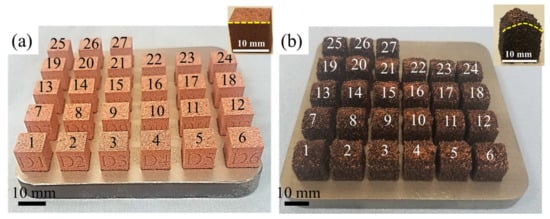
Figure 3.
Photos of laser powder bed fusion additively manufactured (a) Cu and (b) Cu-CNT samples at different manufacturing parameters; process parameters can be found from the number on top of each sample and Figure 1. Insets show close-up view of one of the samples for better comparison.
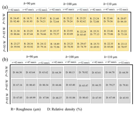
Figure 4.
Relative density and roughness for LPBF-AM (a) Cu and (b) Cu-CNT samples corresponding to their building conditions.
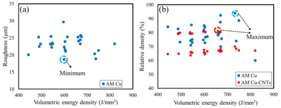
Figure 5.
(a) Average surface roughness and (b) relative density as a function of volumetric energy density for AM Cu and Cu-CNTs.
As seen in Figure 4, the Cu sample fabricated at laser power of 93 W, scanning speed of 47 mm/s, and hatch spacing of 90 µm showed the highest amount of relative density and relatively lower surface roughness; therefore, this sample was used for further characterization.
Jadhav et al. [33] reported that the addition of 0.1 wt.% carbon nanoparticle to pure copper powder increased the laser absorption rate of powders and powder flowability, leading to enhanced relative density of SLM parts. They reported a minimum energy density of 700 J/mm3 to obtain dense SLM parts from pure copper powder and 200–550 J/mm3 for fabrication of dense Cu–carbon nanoparticle parts. In the present study, addition of 0.5 wt.% CNTs to Cu led to formation of parts with maximum relative density of 81%, with both VED and relative density lower than that of Cu. The reason that the same amount of energy was not able to process Cu-CNTs as dense as pure Cu may be due to fact that the laser energy absorbed by the CNT was not efficiently transferred to the Cu particles, due to weak physical interaction and bonding between the CNT and Cu particles. EDS mapping shows distribution of CNTs on the surface of Cu powders. An ideal black body should have emissivity or absorbance of 1.0, which is difficult to attain in practice, especially in a wide spectral range. CNTs can have absorbances of 0.98–0.99 from the far-ultraviolet (200 nm) to far-infrared (200 μm) wavelengths. Theoretically, this means that they can help absorb the laser energy, and theoretically, it should reduce the amount of energy needed to melt the material. However, in this study, the maximum 80% density in Cu-CNT was achieved at all powers (e.g., 76 watt, 47 mm/s, and h = 100 microns). 76 watt was the lowest power that was used. Given that power seems to have insignificant effect on the density, the porosity and low density achieved in fabricating the Cu-CNT composite could have been caused by other factors. The light weight of the CNTs and the laser impact could potentially cause scatter of the CNTs. These sparks and scattering was clearly visible during the build. As CNTs scattered, there were sparks and splatter of the material, which could potentially cause porosity and low density. To avoid these issues, it is suggested that embedding the CNT inside the Cu particles rather than just coating Cu with CNT could result in less porosity and higher density.
The lowest surface roughness for Cu samples was achieved at around 600 J/mm3. Overall, the surface roughness values were found to be very high, particularly for Cu-CNT samples, to the extent that the roughness exceeded the capability of the measuring instruments.
3.3. Microstructure and Elemental Characterization of As-Built Parts
Microstructure characterization of the Cu and Cu-CNT samples fabricated using LPBF-AM at optimal conditions for both the top and bottom surfaces are shown in Figure 6. Insets show the surfaces of interest. This figure indicates the macropore formation for all samples. Several images were used to calculate the amount of porosity. On average, 20+ trials were used for each sample. The amount of porosity was 16% and 11% for the bottom and top surfaces of as-built Cu, respectively, with an average of ~13.5%. Top and bottom surfaces of Cu-CNTs showed porosity of ~17% and 18%, respectively. On average, the Cu-CNT porosity was 17.5%. These results were consistent with the Archimedes density values. To validate the presence of CNTs in as-built Cu-CNTs, EDS mapping of the sample from both surfaces is shown in Figure 7, indicating distribution of CNTs on the surface of Cu powder.
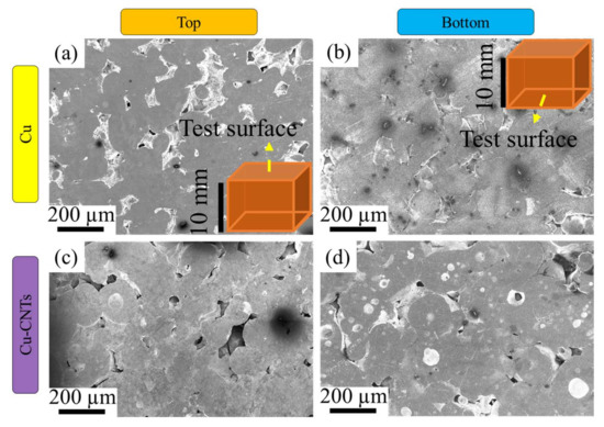
Figure 6.
SEM images of LPBF-AM Cu from (a) top and (b) bottom surfaces; Cu-CNTs from (c) top and (d) bottom surfaces.
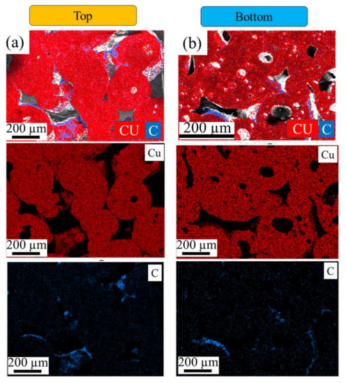
Figure 7.
Energy-dispersive spectroscopy (EDS) mapping of the as-fabricated Cu-CNTs from (a) top and (b) bottom surface showing CNTs distribution on surface of the Cu powders.
3.4. Thermal Conductivity and Electrical Conductivity
The thermal conductivity of Cu and Cu-CNTs, fabricated using laser powder bed fusion additive manufacturing at optimal conditions, was measured as a function of temperature over the range from 298 K to 1073 K and shown in Figure 8. The thermal conductivity of conventionally fabricated Cu as a function of temperature was also shown for comparison [34]. The Cu sample showed thermal conductivity and electrical conductivity of ~108 W/m·K and ~20% IACS, respectively, at room temperature. The thermal conductivity and electrical conductivity of as-built Cu-CNTs were ~85 W/m·K and ~10% IACS at room temperature, respectively. Figure 8 shows that the thermal conductivity of Cu, fabricated using LPBF-AM, decreased to ~15 W/m·K as temperature increased from room temperature to ~773 K. Similar results were found for conventionally fabricated Cu [34,35]. The effect of the phonon on thermal conductivity at high temperatures leads to a decrease in thermal conductivity with increasing temperature because of a reduction in the electron mean free path because of scattering [35]. Thermal conductivity of AM Cu increased to ~70 W/m·K, with a further increase in temperature to 1073 K. This may be attributed to sintering of sample, which reduces the amount of porosity. For AM Cu-CNTs, the change of thermal conductivity was not significant from 298 K to 573 K and it was ~80–85 W/m·K. With a further increase in temperature to 673 K, thermal conductivity raised slightly to ~95 W/m·K, and then decreased to ~12 W/m·K at 973 K and ~45 W/m·K at 1073 K. Overall, as-built Cu-CNTs showed higher thermal conductivity as compared to as-built Cu at a temperature range from 373 K to 873 K.
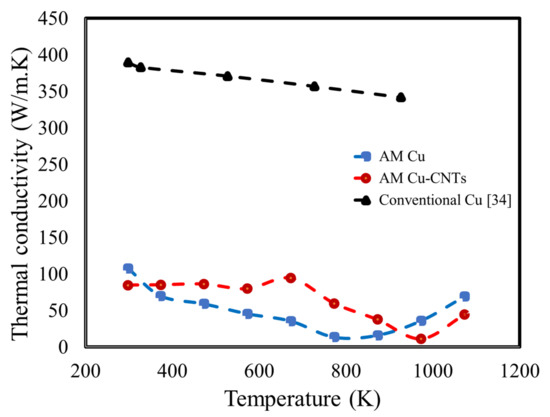
Figure 8.
Thermal conductivity as a function of temperature for as-built Cu and Cu-CNTs as compared to conventionally fabricated Cu [34].
Copper is often used for its high thermal conductivity in different applications. Having higher thermal conductivity may be desirable in some applications. However, lower conductivity could potentially be very helpful in sustaining the melt pool in additive manufacturing, making fabrication of Cu and Cu-CNT materials easier. High conductivity usually results in rapid dissipation that could become problematic and require very high power in fabricating Cu- and Cu-CNT. Lower conductivity will help with reducing the amount of power that is needed for fabrication of Cu.
4. Discussion
Additive manufacturing is a process that relies heavily on the thermos-physical properties of the material. The process involves heat deposition, melting, and heat dissipation. A successful process consists of a process that can deliver enough heat to the surface of the material to consistently and continuously melt the material as the laser or electron beam moves across the sample. Because of this, heat dissipation plays an important role. Faster heat dissipation results in faster cooling rates, changing not only the consistency of the melt but also the microstructure of the melt. The heat dissipation depends on the thermos-physical properties of the material. Therefore, it is important to understand the energy balance and its relationship with the thermo-physical properties of the material.
In an open system that involves phase change of the material, the energy balance equation can be written as follows [3]:
In this equation, H is enthalpy, KE is the kinetic energy, PE is the potential energy, Q is the heat, and W is the work done on the system. This equation essentially states that the total work done on a system and total heat input to the system will add to the enthalpy, potential, or kinetic energy of the system. In a case where we deal with materials phase change, the work done on a system is negligible, and change in potential and kinetic energy is insignificant, such as the case with laser melting, and the energy balance is simplified to the following equation:
In melting and solidification, ΔH becomes equivalent to ΔHm, which is the latent heat of fusion, or the energy required to melt or solidify the material at certain temperature and pressure. In this case, the rate of heat input is equal to the rate of change in enthalpy, as follows:
This equation is illustrated graphically in Figure 9. In this equation, QL is the laser energy delivered to the melt pool, QR is the heat loss due to radiation, Qconv is the heat loss due to convection, and Qcond is the heat loss due to conduction. In many cases where the process is conducted in a vacuum, the convection heat loss is ignored. If Qcond and QR are large, QL must increase proportionally so that melting can occur. This is challenging in Cu because of Cu’s large conductivity that increases the Qcond, as well as its large reflectivity. The summation of the absorptivity, reflectivity, and transmissivity in the material is 1 at any wavelength:
where α is the absorptivity, τ is the transmissivity, and ρ is the reflectivity at a certain wavelength denoted by subscript λ. As can be seen in Figure 10, the absorptivity of Cu is very low at the wavelength typically used in laser melting systems (YAG laser with 1.06 μm). Because of low absorptivity and high reflectivity of Cu at this wavelength, QR must be large. Recent advancements in Green Laser have resulted in machines that can use a YAG laser with 500 nm wavelength. This type of laser is more appropriate for very conductive materials such as Cu and Ag.
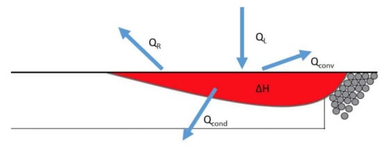
Figure 9.
Energy balance for the melt pool [4].
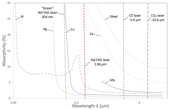
Figure 10.
Absorptivity for different materials. The wavelength of different types of laser are shown in the vertical dash lined intercept [5].
Theoretically, based on this energy equation, as the energy per volume density increases, more energy exists for melting of the Cu and better melting and solidification should occur. This was shown in previous studies, where higher energy densities resulted in better melting and formation of line scans in Inconel [16]. However, a closer look at Figure 5b shows that the optimal density occurs at energy levels of 700 and 630 J/mm3. This could potentially be argued that as more heat is absorbed by the Cu powder, and melt pool reaches higher temperatures above the melting point, the thermal conductivity of the powder also increases. This is clearly seen in Figure 8 as the measured thermal conductivity of both Cu and Cu-CNT material increases above 900 K and 1000 K in Cu and Cu-CNT, respectively. This trend could potentially continue at higher temperatures and above melt, impacting a larger area around the melt pool and therefore allowing for a large amount of heat to dissipate from the melt pool due to higher conductivities. This could result in faster heat removal from the melt pool and heat dissipation that counters the higher absorption effect.
Effect of Manufacturing and CNT Addition on Thermal Conductivity and Electrical Conductivity of As-Built Samples
The current samples fabricated using LPBF-AM showed lower thermal and electrical conductivity value than the value reported for pure Cu (~326–400 W/m.K, 95–100% IACS) and Cu-CNT composites (~276 W/m.K, 85% IACS) fabricated using conventional method [2,34,36]. This may be due to porous structure of as-built Cu and Cu-CNTs. The porosities act as insulation sites, reducing the conductivity of the components [37]. Other factors such as grain size, thermal and electrical resistance at the grain boundaries, residual stresses, and impurities may also contribute to the lowering of thermal conductivity and electrical conductivity [29,33]. Low electrical conductivity of 39% IACS was also reported for SLM Cu + C0.1 sample due to the formation of a copper–phosphorus solid-solution after SLM. Furthermore, the decrease in thermal and electrical conductivity of Cu with addition of CNTs at room temperature may be due to the generating of additional interfaces, which increase thermal resistance and negatively affect the electrical and thermal conductivity of the composite [36].
5. Conclusions
As shown in the Discussion section, thermal conductivity is an extremely important characteristics that dictates how successful an additive process is. If the material is extremely conductive, sustaining the melt pool is very challenging. Copper is one of the most conductive materials that currently exists. The additive manufacturing community has been struggling with fabricating copper mainly due to its high conductivity. Adding CNTs can effectively change the conductivity of the copper and allow sustainment of the melt pool. Copper–carbon nanotubes composites were successfully fabricated via laser powder bed fusion additive manufacturing with a moderate laser power (100 W) for the first time. The relative density, surface roughness, and thermal conductivity were evaluated and compared with pure copper fabricated with the same technique. The results showed that the addition of 0.5 wt.% CNTs reduced the maximum relative density from 94% for pure copper to 81% for Cu-CNTs composite. Furthermore, a surface as rough as 1 mm was obtained for as-built Cu-CNTs as compared to 18 µm for as-built pure copper. The printing parameters played critical roles in controlling the printing quality. A combination of high relative density and low surface roughness was achieved at a laser power of 93 W, a scanning speed of 47 mm/s, and a hatch spacing of 90 µm, corresponding to volumetric energy density (VED) of 730 J/mm3 for pure copper. The optimal condition for Cu-CNTs was a laser power of 93 W, a scanning speed of 47 mm/s, and a hatch spacing of 100 µm (VED: 660 J/mm3). The printed Cu and Cu-CNTs parts exhibited thermal conductivity of 108 W/m.K and 85 W/m.K at room temperature, respectively, which was much lower than the bulk Cu and Cu-CNTs fabricated using a traditional process due to its porous structure. The electrical conductivity was also ~20% IACS for as-built Cu, which decreased to ~10% IACS with the addition of 0.5 wt.% CNTs due to additional interfaces, which increase thermal resistance.
Author Contributions
Conceptualization, L.L., process visualization, LL, Methods, LL, Review and Revisions, LL, Conducting the Experiments, M.S., Writing the first Draf, M.S., Conducting Experiments such as Milling, J.R., Review and Revise, J.R., Analysis of the Results, J.R. All authors have read and agreed to the published version of the manuscript.
Funding
This research received no external funding.
Institutional Review Board Statement
Not applicable.
Informed Consent Statement
Not applicable.
Acknowledgments
The authors acknowledge the Eyring Materials Center at ASU for access to advanced characterization techniques. The authors also acknowledge the Innovation Hub in Polytechnic School campus, ASU for additive manufacturing of the samples. Additionally, authors thanks Shane Tokishi for conducting the image J analysis for the samples.
Conflicts of Interest
The authors declare no conflict of interest.
References
- Caiazzo, F.; Campanelli, S.L.; Cardaropoli, F.; Contuzzi, N.; Sergi, V.; Ludovico, A.D. Manufacturing and characterization of similar to foam steel components processed through selective laser melting. Int. J. Adv. Manuf. Technol. 2017, 92, 2126–2130. [Google Scholar] [CrossRef]
- Jiang, Q.; Zhang, P.; Yu, Z.; Shi, H.; Wu, D.; Yan, H.; Ye, X.; Lu, Q.; Tian, Y. A Review on Additive Manufacturing of Pure Copper. Coatings 2021, 11, 740. [Google Scholar] [CrossRef]
- Jadhav, S.; Dadbakhsh, S.; Goossens, L.; Kruth, J.-P.; Van Humbeeck, J.; Vanmeensel, K. Influence of selective laser melting process parameters on texture evolution in pure copper. J. Mater. Process. Technol. 2019, 270, 47–58. [Google Scholar] [CrossRef]
- Ladani, L. Local and Global Mechanical Behavior and Microstructure of Ti6Al4V Parts Built Using Electron Beam Melting Technology. Met. Mater. Trans. A 2015, 46, 3835–3841. [Google Scholar] [CrossRef]
- Ladani, L. Additive Manufacturing of Metals: Materials, Processes, Tests, and Standards; DEStech Publications: Lancaster, PA, USA, 2020. [Google Scholar]
- Ladani, L.; Sadeghilaridjani, M. Review of Powder Bed Fusion Additive Manufacturing for Metals. Metals 2021, 11, 1391. [Google Scholar] [CrossRef]
- Ahsan, F.; Ladani, L. Temperature Profile, Bead Geometry, and Elemental Evaporation in Laser Powder Bed Fusion Additive Manufacturing Process. JOM 2019, 72, 429–439. [Google Scholar] [CrossRef]
- Andreotta, R.; Ladani, L.; Brindley, W. Finite element simulation of laser additive melting and solidification of Inconel 718 with experimentally tested thermal properties. Finite Elements Anal. Des. 2017, 135, 36–43. [Google Scholar] [CrossRef]
- Ahsan, F.; Razmi, J.; Ladani, L. Multi-Physics Modeling of Laser Interaction with Surface in Powder Bed Melting Process. In Proceedings of the ASME 2018 International Mechanical Engineering Congress and Exposition, Pittsburgh, PA, USA, 9–15 November 2018; Volume 2. [Google Scholar] [CrossRef]
- Romano, J.; Ladani, L.; Sadowski, M. Laser Additive Melting and Solidification of Inconel 718: Finite Element Simulation and Experiment. JOM 2016, 68, 967–977. [Google Scholar] [CrossRef]
- Romano, J.; Ladani, L.; Sadowski, M. Thermal Modeling of Laser Based Additive Manufacturing Processes within Common Materials. Procedia Manuf. 2015, 1, 238–250. [Google Scholar] [CrossRef]
- Keshavarzkermani, A.; Sadowski, M.; Ladani, L. Direct metal laser melting of Inconel 718: Process impact on grain formation and orientation. J. Alloy. Compd. 2018, 736, 297–305. [Google Scholar] [CrossRef]
- Mian, J.; Razmi, J.; Ladani, L. Defect analysis and fatigue strength prediction of as-built Ti6Al4V parts, produced using electron beam melting (EBM) AM technology. Materialia 2021, 16, 101041. [Google Scholar] [CrossRef]
- Ladani, L.; Razmi, J.; Choudhury, S.F. Mechanical Anisotropy and Strain Rate Dependency Behavior of Ti6Al4V Produced Using E-Beam Additive Fabrication. J. Eng. Mater. Technol. 2014, 136, 031006. [Google Scholar] [CrossRef]
- Mian, J.; Razmi, J.; Ladani, L. Mechanical Behavior of Electron Beam Powder Bed Fusion Additively Manufactured Ti6Al4V Parts at Elevated Temperatures. J. Manuf. Sci. Eng. 2020, 143, 1–24. [Google Scholar] [CrossRef]
- Ladani, L.; Romano, J.; Brindley, W.; Burlatsky, S. Effective liquid conductivity for improved simulation of thermal transport in laser beam melting powder bed technology. Addit. Manuf. 2017, 14, 13–23. [Google Scholar] [CrossRef]
- Sadowski, M.; Ladani, L.; Brindley, W.; Romano, J. Optimizing quality of additively manufactured Inconel 718 using powder bed laser melting process. Addit. Manuf. 2016, 11, 60–70. [Google Scholar] [CrossRef]
- Romano, J.; Ladani, L.; Razmi, J.; Sadowski, M. Temperature distribution and melt geometry in laser and electron-beam melting processes—A comparison among common materials. Addit. Manuf. 2015, 8, 1–11. [Google Scholar] [CrossRef]
- Shanmugasundaram, S.A.; Razmi, J.; Mian, J.; Ladani, L. Mechanical Anisotropy and Surface Roughness in Additively Manufactured Parts Fabricated by Stereolithography (SLA) Using Statistical Analysis. Materials 2020, 13, 2496. [Google Scholar] [CrossRef]
- Sundaram, R.M.; Sekiguchi, A.; Sekiya, M.; Yamada, T.; Hata, K. Copper/carbon nanotube composites: Research trends and outlook. R. Soc. Open Sci. 2018, 5, 180814. [Google Scholar] [CrossRef]
- Ladani, L. Multi-Scale Manufacturing of Carbon Nanotube Composites. U.S. Patent No. 15/684,455, 23 August 2016. [Google Scholar]
- Awad, I.; Ladani, L. Mechanical integrity of a carbon nanotube/copper-based through-silicon via for 3D integrated circuits: A multi-scale modeling approach. Nanotechnology 2015, 26, 485705. [Google Scholar] [CrossRef]
- Ladani, L.; Awad, I.; She, Y.; Dardona, S.; Schmidt, W. Fabrication of carbon nanotube/copper and carbon nanofiber/copper composites for microelectronics. Mater. Today Commun. 2017, 11, 123–131. [Google Scholar] [CrossRef]
- Wang, P.; Zhang, B.; Tan, C.C.; Raghavan, S.; Lim, Y.-F.; Sun, C.-N.; Wei, J.; Chi, D. Microstructural characteristics and mechanical properties of carbon nanotube reinforced Inconel 625 parts fabricated by selective laser melting. Mater. Des. 2016, 112, 290–299. [Google Scholar] [CrossRef]
- Wang, Z.; Ren, R.; Song, H.; Jia, X. Improved tribological properties of the synthesized copper/carbon nanotube nanocomposites for rapeseed oil-based additives. Appl. Surf. Sci. 2018, 428, 630–639. [Google Scholar] [CrossRef]
- Zhu, H.; Lu, L.; Fuh, J. Development and characterisation of direct laser sintering Cu-based metal powder. J. Mater. Process. Technol. 2003, 140, 314–317. [Google Scholar] [CrossRef]
- Silbernagel, C.; Gargalis, L.; Ashcroft, I.; Hague, R.; Galea, M.; Dickens, P. Electrical resistivity of pure copper processed by medium-powered laser powder bed fusion additive manufacturing for use in electromagnetic applications. Addit. Manuf. 2019, 29, 100831. [Google Scholar] [CrossRef]
- Raab, S.J.; Guschlbauer, R.; Lodes, M.A.; Körner, C. Thermal and Electrical Conductivity of 99.9% Pure Copper Processed via Selective Electron Beam Melting. Adv. Eng. Mater. 2016, 18, 1661–1666. [Google Scholar] [CrossRef]
- Kumar, A.Y.; Wang, J.; Bai, Y.; Huxtable, S.T.; Williams, C.B. Impacts of process-induced porosity on material properties of copper made by binder jetting additive manufacturing. Mater. Des. 2019, 182, 108001. [Google Scholar] [CrossRef]
- Ahsan, F.; Razmi, J.; Ladani, L. Experimental measurement of thermal diffusivity, conductivity and specific heat capacity of metallic powders at room and high temperatures. Powder Technol. 2020, 374, 648–657. [Google Scholar] [CrossRef]
- Liu, Z.; Xu, S.; Xiao, B.; Xue, P.; Wang, W.; Ma, Z. Effect of ball-milling time on mechanical properties of carbon nanotubes reinforced aluminum matrix composites. Compos. Part A Appl. Sci. Manuf. 2012, 43, 2161–2168. [Google Scholar] [CrossRef]
- Constantin, L.; Wu, Z.; Li, N.; Fan, L.; Silvain, J.-F.; Lu, Y.F. Laser 3D printing of complex copper structures. Addit. Manuf. 2020, 35, 101268. [Google Scholar] [CrossRef]
- Jadhav, S.D.; Dadbakhsh, S.; Vleugels, J.; Hofkens, J.; Van Puyvelde, P.; Yang, S.; Kruth, J.-P.; Van Humbeeck, J.; Vanmeensel, K. Influence of Carbon Nanoparticle Addition (and Impurities) on Selective Laser Melting of Pure Copper. Materials 2019, 12, 2469. [Google Scholar] [CrossRef]
- Sobamowo, G.M.; Ibrahim, S.A.; Salami, M.O. A Study on Thermal Performance of Palladium as Material for Passive Heat Transfer Enhancement Devices in Thermal and Electronics Systems. Semicond. Sci. Inf. Devices 2020, 2, 15–24. [Google Scholar] [CrossRef]
- Rho, H.; Lee, S.; Bae, S.; Kim, T.-W.; Lee, D.S.; Lee, H.J.; Hwang, J.Y.; Jeong, T.; Kim, S.; Ha, J.-S.; et al. Three-Dimensional Porous Copper-Graphene Heterostructures with Durability and High Heat Dissipation Performance. Sci. Rep. 2015, 5, 12710. [Google Scholar] [CrossRef]
- Van Duong, L.; Anh, N.N.; Trung, T.B.; Chung, L.D.; Huan, N.Q.; Nhung, D.T.; Phuong, M.T.; Minh, P.N.; Phuong, D.D.; Van Trinh, P. Effect of annealing temperature on electrical and thermal property of cold-rolled multi-walled carbon nanotubes reinforced copper composites. Diam. Relat. Mater. 2020, 108, 107980. [Google Scholar] [CrossRef]
- Uddin, S.M.; Mahmud, T.; Wolf, C.; Glanz, C.; Kolaric, I.; Volkmer, C.; Höller, H.; Wienecke, U.; Roth, S.; Fecht, H.-J. Effect of size and shape of metal particles to improve hardness and electrical properties of carbon nanotube reinforced copper and copper alloy composites. Compos. Sci. Technol. 2010, 70, 2253–2257. [Google Scholar] [CrossRef]


Publisher’s Note: MDPI stays neutral with regard to jurisdictional claims in published maps and institutional affiliations. |
© 2022 by the authors. Licensee MDPI, Basel, Switzerland. This article is an open access article distributed under the terms and conditions of the Creative Commons Attribution (CC BY) license (https://creativecommons.org/licenses/by/4.0/).