Thermal Analysis and Operational Characteristics of an AlGaN/GaN High Electron Mobility Transistor with Copper-Filled Structures: A Simulation Study


Abstract
:1. Introduction
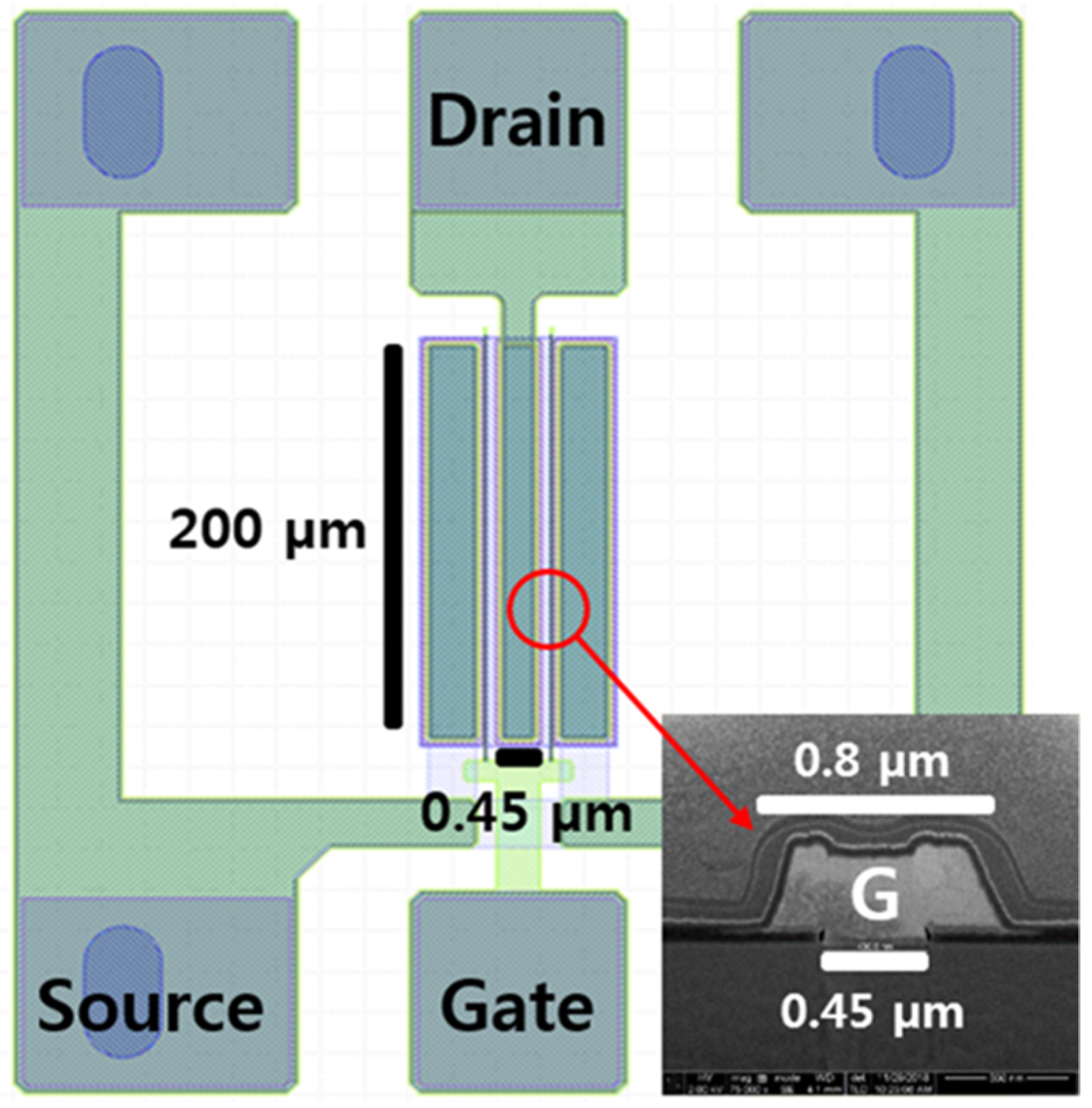
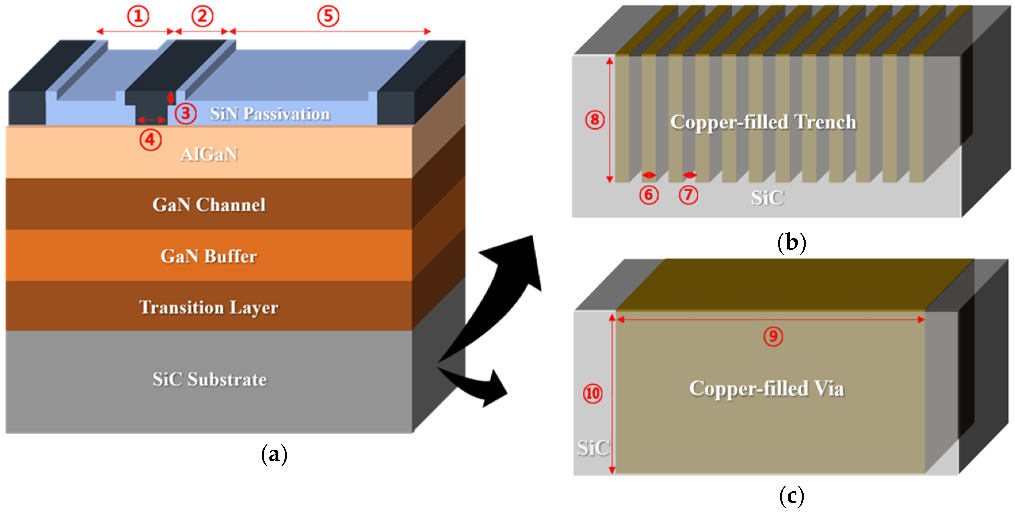
2. Materials and Methods
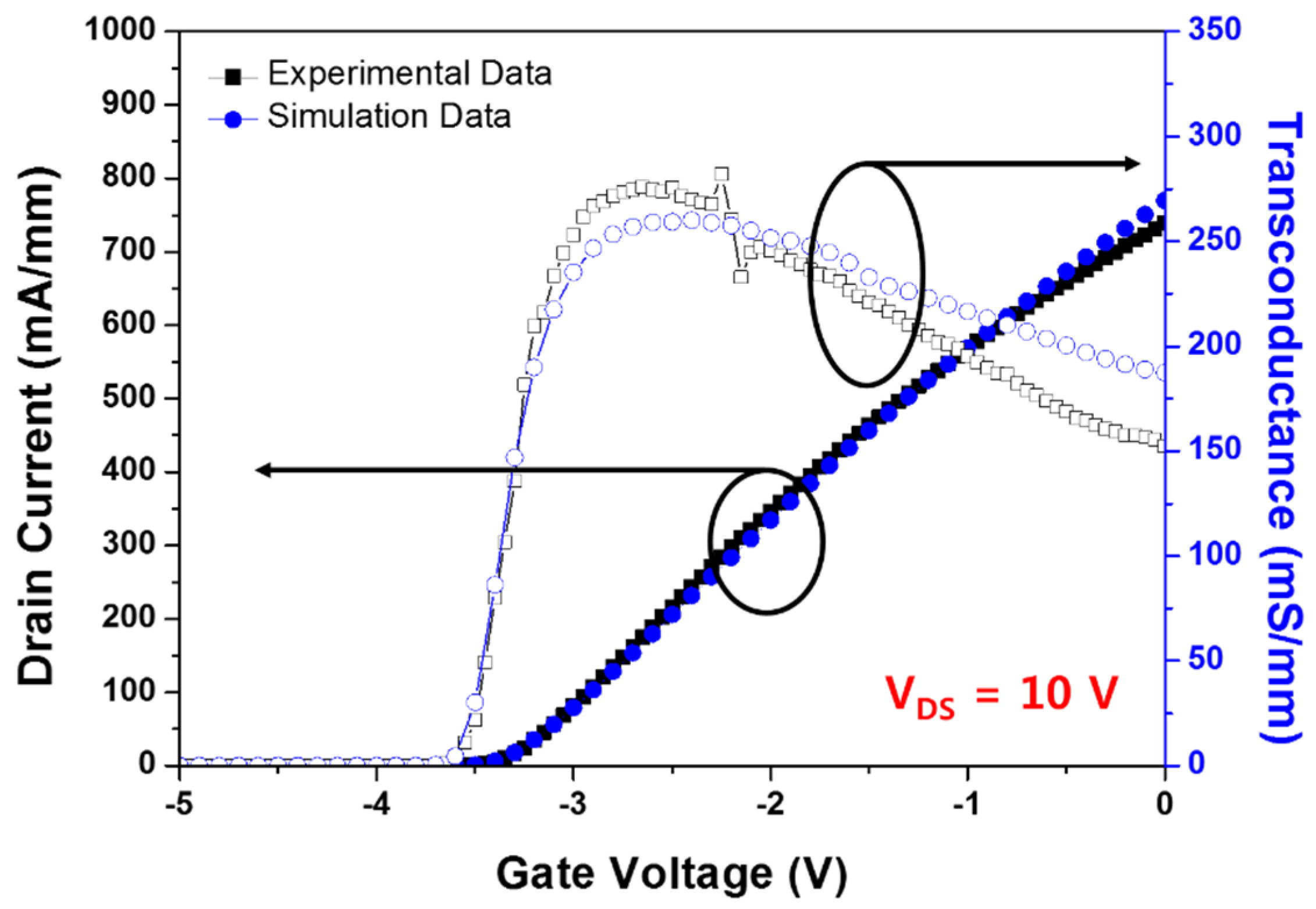
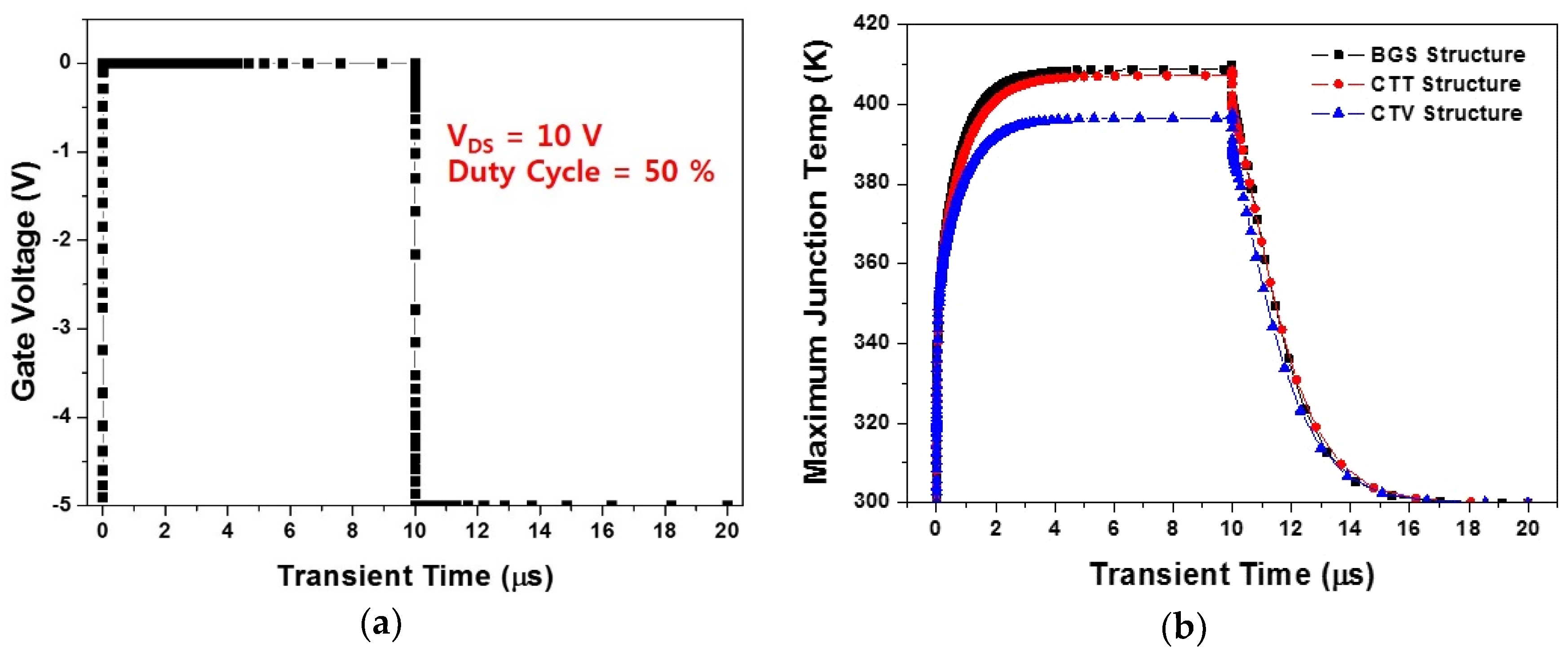
3. Results and Discussions
4. Conclusions
Author Contributions
Funding
Conflicts of Interest
References
- Shen, L.; Heikman, S.; Moran, B.; Coffie, R.; Zhang, N.Q.; Buttari, D.; Smorchkova, I.P.; Keller, S.; DenBaars, S.P.; Mishra, U.K. AlGaN/AlN/GaN high-power microwave HEMT. IEEE Electron Device Lett. 2001, 22, 457–459. [Google Scholar] [CrossRef]
- Del Alamo, J.A.; Joh, J. GaN HEMT reliability. Microelectron. Reliab. 2009, 49, 1200–1206. [Google Scholar] [CrossRef]
- Mishra, U.K.; Parikh, P.; Wu, Y.F. AlGaN/GaN HEMTs-an overview of device operation and applications. Proc. IEEE 2002, 90, 1022–1031. [Google Scholar] [CrossRef] [Green Version]
- Lu, W.; Yang, J.; Khan, M.A.; Adesida, I. AlGaN/GaN HEMTs on SiC with over 100 GHz f/sub T/and low microwave noise. IEEE Trans. Electron Devices 2001, 48, 581–585. [Google Scholar] [CrossRef]
- Gaska, R.; Osinsky, A.; Yang, J.W.; Shur, M.S. Self-heating in high-power AlGaN-GaN HFETs. IEEE Electron Device Lett. 1998, 19, 89–91. [Google Scholar] [CrossRef]
- Wang, X.D.; Hu, W.D.; Chen, X.S.; Lu, W. The study of self-heating and hot-electron effects for AlGaN/GaN double-channel HEMTs. IEEE Trans. Electron Devices 2012, 59, 1393–1401. [Google Scholar] [CrossRef]
- Sadi, T.; Kelsall, R.W.; Pilgrim, N.J. Investigation of self-heating effects in submicrometer GaN/AlGaN HEMTs using an electrothermal Monte Carlo method. IEEE Trans. Electron Devices 2006, 53, 2892–2900. [Google Scholar] [CrossRef]
- Hwang, I.T.; Jang, K.W.; Kim, H.J.; Lee, S.H.; Lim, J.W.; Yang, J.M.; Kwon, H.S.; Kim, H.S. Analysis of DC Characteristics in GaN-Based Metal-Insulator-Semiconductor High Electron Mobility Transistor with Variation of Gate Dielectric Layer Composition by Considering Self-Heating Effect. Appl. Sci. 2019, 9, 3610. [Google Scholar] [CrossRef] [Green Version]
- Kwak, H.T.; Chang, S.B.; Jung, H.G.; Kim, H.S. Thermal analysis of AlGaN/GaN high-electron-mobility transistor and its RF power efficiency optimization with source-bridged field-plate structure. J. Nanosci. Nanotechnol. 2018, 18, 5860–5867. [Google Scholar] [CrossRef]
- Kwak, H.T.; Jang, K.W.; Kim, H.J.; Lee, S.H.; Lim, J.W.; Kim, H.S. DC Characteristics of AlGaN/GaN High-Electron Mobility Transistor with a Bottom Plate Connected to Source-Bridged Field Plate Structure. J. Nanosci. Nanotechnol. 2019, 19, 2319–2322. [Google Scholar] [CrossRef]
- Wang, A.; Tadjer, M.J.; Calle, F. Simulation of thermal management in AlGaN/GaN HEMTs with integrated diamond heat spreaders. Semicond. Sci. Technol. 2013, 28, 055010. [Google Scholar] [CrossRef]
- Kim, H.J.; Jang, K.W.; Kim, H.S. Operational Characteristics of Various AlGaN/GaN High Electron Mobility Transistor Structures Concerning Self-Heating Effect. J. Nanosci. Nanotechnol. 2019, 19, 6016–6022. [Google Scholar] [CrossRef] [PubMed]
- Kwak, H.T.; Chang, S.B.; Kim, H.J.; Jang, K.W.; Yoon, H.; Lee, S.H.; Lim, J.W.; Kim, H.S. Operational Improvement of AlGaN/GaN High Electron Mobility Transistor by an Inner Field-Plate Structure. Appl. Sci. 2018, 8, 974. [Google Scholar] [CrossRef] [Green Version]
- Yan, Z.; Liu, G.; Khan, J.M.; Balandin, A.A. Graphene quilts for thermal management of high-power GaN transistors. Nat. Commun. 2012, 3, 827. [Google Scholar] [CrossRef]
- Hwang, Y.H.; Kang, T.S.; Ren, F.; Pearton, S.J. A novel approach to improve heat dissipation of AlGaN/GaN high electron mobility transistors with a backside Cu via. ECS Trans. 2015, 66, 223–230. [Google Scholar] [CrossRef]
- Chai, Y.; Zhang, K.; Zhang, M.; Chan, P.C.H.; Yuen, M.M.F. Carbon nanotube/copper composites for via filling and thermal management. In Proceedings of the 57th Electronic Components and Technology Conference, Reno, NV, USA, 29 May–1 June 2007; pp. 1224–1229. [Google Scholar]
- Won, Y.; Cho, J.; Agonafer, D.; Asheghi, M.; Goodson, K.E. Cooling limits for GaN HEMT technology. In Proceedings of the 2013 IEEE Compound Semiconductor Integrated Circuit Symposium (CSICS), Monterey, CA, USA, 13–16 October 2013. [Google Scholar]
- Poust, B.; Gambin, V.; Sandhu, R.; Smorchkova, I.; Lewis, G.; Elmadjian, R.; Li, D.; Geiger, C.; Heying, B.; Wojtowicz, M.; et al. Selective growth of diamond in thermal vias for GaN HEMTs. In Proceedings of the 2013 IEEE Compound Semiconductor Integrated Circuit Symposium (CSICS), Monterey, CA, USA, 13–16 October 2013. [Google Scholar]
- Beica, R.; Sharbono, C.; Ritzdorf, T. Through silicon via copper electrodeposition for 3D integration. In Proceedings of the 2008 58th Electronic Components and Technology Conference, Lake Buena Vista, FL, USA, 27–30 May 2008; pp. 577–583. [Google Scholar]
- Baskaran, R.; Hanson, A.W. Simulation of the impact of through-substrate vias on the thermal resistance of compound semiconductor devices. In Proceedings of the 2015 International Conference on Compound Semiconductor Manufacturing Technology (CS MANTECH 2015), Scottsdale, AZ, USA, 18–21 May 2015; pp. 163–166. [Google Scholar]
- Sugie, R.; Kosaka, K.; Seki, H.; Hashimoto, H.; Yoshikawa, M. Measurement of temperature-dependent stress in copper-filled silicon vias using polarized Raman spectroscopy. J. Appl. Phys. 2013, 114, 233503. [Google Scholar] [CrossRef]
- Inoue, S.; Okamoto, K.; Matsuki, N.; Kim, T.W.; Fujioka, H. Epitaxial growth of GaN on copper substrates. Appl. Phys. Lett. 2006, 88, 261910. [Google Scholar] [CrossRef]
- Ohta, J.; Fujioka, H.; Takahashi, H.; Oshima, M. Growth of epitaxial AlN films on (Mn, Zn) Fe2O4 substrates by pulsed laser deposition. Appl. Surf. Sci. 2002, 197, 486–489. [Google Scholar] [CrossRef]
- Kawaguchi, Y.; Ohta, J.; Kobayashi, A.; Fujioka, H. Room-temperature epitaxial growth of GaN on lattice-matched ZrB 2 substrates by pulsed-laser deposition. Appl. Phys. Lett. 2005, 87, 221907. [Google Scholar] [CrossRef]
- Kato, S.; Satoh, Y.; Sasaki, H.; Masayuki, I.; Yoshida, S. C-doped GaN buffer layers with high breakdown voltages for high-power operation AlGaN/GaN HFETs on 4-in Si substrates by MOVPE. J. Cryst. Growth 2007, 298, 831–834. [Google Scholar] [CrossRef]
- Keblinski, P.; Phillpot, S.R.; Choi, S.U.S.; Eastman, J.A. Mechanisms of heat flow in suspensions of nano-sized particles (nanofluids). Int. J. Heat Mass Transfer 2002, 45, 855–863. [Google Scholar] [CrossRef]
- Cahill, D.G.; Braun, P.V.; Chen, G.; Clarke, D.R.; Fan, S.; Goodson, K.E.; Keblinski, P.; King, W.P.; Mahan, G.D.; Majumdar, A.; et al. Nanoscale thermal transport. II. 2003–2012. Appl. Phys. Rev. 2014, 1, 011305. [Google Scholar] [CrossRef] [Green Version]
- Schubert, T.; Trindade, B.; Weißgärber, T.; Kieback, B. Interfacial design of Cu-based composites prepared by powder metallurgy for heat sink applications. Mater. Sci. Eng. A 2008, 475, 39–44. [Google Scholar] [CrossRef] [Green Version]
- Brendel, A.; Popescu, C.; Leyens, C.; Woltersdorf, J.; Pippel, E.; Bolt, H. SiC-fibre reinforced copper as heat sink material for fusion applications. J. Nuclear Mater. 2004, 329, 804–808. [Google Scholar] [CrossRef]
- Tekce, H.S.; Kumlutas, D.; Tavman, I.H. Effect of particle shape on thermal conductivity of copper reinforced polymer composites. J. Reinf. Plast. Compos. 2007, 26, 113–121. [Google Scholar] [CrossRef]
- Manoi, A.; Pomeroy, J.W.; Killat, N.; Kuball, M. Benchmarking of thermal boundary resistance in AlGaN/GaN HEMTs on SiC substrates: Implications of the nucleation layer microstructure. IEEE Electron Device Lett. 2010, 31, 1395–1397. [Google Scholar] [CrossRef]
- Riedel, G.J.; Pomeroy, J.W.; Hilton, K.P.; Maclean, J.O.; Wallis, D.J.; Uren, M.J.; Martin, T.; Forsberg, U.; Lundskog, A.; Kakanakova-Georgieva, A.; et al. Reducing thermal resistance of AlGaN/GaN electronic devices using novel nucleation layers. IEEE Electron Device Lett. 2008, 30, 103–106. [Google Scholar] [CrossRef]
- Silvaco, Inc. Selberherr’s Impact Ionization Model. In Atlas User’s Manual Device Simulation Software; Silvaco Inc.: Santa Clara, CA, USA, 2016; pp. 237–240. [Google Scholar]
- Selberherr, S. MOS device modeling at 77 K. IEEE Trans. Electron Devices 1989, 36, 1464–1474. [Google Scholar] [CrossRef]
- Kuball, M.; Riedel, G.J.; Pomeroy, J.W.; Sarua, A.; Uren, M.J.; Martin, T.; Hilton, K.P.; Maclean, J.O.; Wallis, D.J. Time-resolved temperature measurement of AlGaN/GaN electronic devices using micro-Raman spectroscopy. IEEE Electron Device Lett. 2007, 28, 86–89. [Google Scholar] [CrossRef]
- Pavlidis, G.; Kendig, D.; Heller, E.R.; Graham, S. Transient thermal characterization of AlGaN/GaN HEMTs under pulsed biasing. IEEE Trans. Electron Devices 2018, 65, 1753–1758. [Google Scholar] [CrossRef]
- Xu, J.; Yin, W.Y.; Mao, J. Transient thermal analysis of GaN heterojunction transistors (HFETs) for high-power applications. IEEE Microw. Wirel. Compon. Lett. 2007, 17, 55–57. [Google Scholar] [CrossRef]


| Parameter | Unit | Value |
|---|---|---|
| ① LGate-Source | μm | 1.025 |
| ② LGate-Head | μm | 0.8 |
| ③ LGate-Foot | nm | 250 |
| ④ LGate | μm | 0.45 |
| ⑤ LGate-Drain | μm | 4.525 |
| ⑥ LCTT-Cu-width | μm | 0.25 |
| ⑦ LCu-Cu | μm | 0.25 |
| ⑧ LCTT-Cu-depth | μm | 5.5 |
| ⑨ LCTV-Cu-width | μm | 6 |
| ⑩ LCTV-Cu-depth | μm | 8 |
| SiN passivation (AlGaN interface) | nm | 90 |
| SiN passivation (gate and side wall) | nm | 40 |
| AlGaN | nm | 25 |
| GaN channel | nm | 50 |
| GaN buffer | μm | 2 |
| Transition layer | nm | 50 |
| SiC substrate | μm | 8 |
| Parameter | Unit | GaN | AlGaN |
|---|---|---|---|
| Bandgap energy | eV | 3.39 | 3.87 |
| Electron affinity | eV | 4 | 2.73 |
| Relative permittivity | - | 9.5 | 9.38 |
| Low field electron mobility | cm2/V·s | 1460 | 300 |
| High field mobility model | - | GANSAT Mobility Model | |
| Electron saturation velocity | cm/s | 1.9 × 10⁷ | 1.12 × 10⁷ |
| Hole saturation velocity | cm/s | 1.9 × 10⁷ | 1.0 × 10⁶ |
| Shockley–Read–Hall (SRH) life time | s | 1.0 × 10⁻⁸ | 1.0 × 10⁻⁸ |
| Parameter | Unit | GaN | AlGaN | SiC | Cu |
|---|---|---|---|---|---|
| Thermal conductivity constant (TC.CONST) | W/cm·K | 1.3 | 0.4 | 3.3 | 3.83 |
| Thermal conductivity factor (TC.NPOW) | - | 0.43 | 0 | 1.61 | 0.3 |
© 2019 by the authors. Licensee MDPI, Basel, Switzerland. This article is an open access article distributed under the terms and conditions of the Creative Commons Attribution (CC BY) license (http://creativecommons.org/licenses/by/4.0/).
Share and Cite
Jang, K.-W.; Hwang, I.-T.; Kim, H.-J.; Lee, S.-H.; Lim, J.-W.; Kim, H.-S. Thermal Analysis and Operational Characteristics of an AlGaN/GaN High Electron Mobility Transistor with Copper-Filled Structures: A Simulation Study. Micromachines 2020, 11, 53. https://doi.org/10.3390/mi11010053
Jang K-W, Hwang I-T, Kim H-J, Lee S-H, Lim J-W, Kim H-S. Thermal Analysis and Operational Characteristics of an AlGaN/GaN High Electron Mobility Transistor with Copper-Filled Structures: A Simulation Study. Micromachines. 2020; 11(1):53. https://doi.org/10.3390/mi11010053
Chicago/Turabian StyleJang, Kyu-Won, In-Tae Hwang, Hyun-Jung Kim, Sang-Heung Lee, Jong-Won Lim, and Hyun-Seok Kim. 2020. "Thermal Analysis and Operational Characteristics of an AlGaN/GaN High Electron Mobility Transistor with Copper-Filled Structures: A Simulation Study" Micromachines 11, no. 1: 53. https://doi.org/10.3390/mi11010053
APA StyleJang, K.-W., Hwang, I.-T., Kim, H.-J., Lee, S.-H., Lim, J.-W., & Kim, H.-S. (2020). Thermal Analysis and Operational Characteristics of an AlGaN/GaN High Electron Mobility Transistor with Copper-Filled Structures: A Simulation Study. Micromachines, 11(1), 53. https://doi.org/10.3390/mi11010053