Article

Chemical Vapor Deposition of Uniform and Large-Domain Molybdenum Disulfide Crystals on Glass/Al2O3 Substrates

1
School of Electronic Information, University of Electronic Science and Technology of China Zhongshan Institute, Zhongshan 528402, China
2
College of Physical Science and Technology, Xiamen University, Xiamen 361005, China
3
School of Information and Communication Engineering, University of Electronic Science and Technology of China, Chengdu 611731, China
*
Author to whom correspondence should be addressed.
Nanomaterials 2022, 12(15), 2719; https://doi.org/10.3390/nano12152719
Submission received: 22 July 2022 / Revised: 1 August 2022 / Accepted: 3 August 2022 / Published: 7 August 2022

Abstract

:
Two-dimensional molybdenum disulfide (MoS2) has attracted significant attention for next-generation electronics, flexible devices, and optical applications. Chemical vapor deposition is the most promising route for the production of large-scale, high-quality MoS2 films. Recently, the chemical vapor deposition of MoS2 films on soda-lime glass has attracted great attention due to its low cost, fast growth, and large domain size. Typically, a piece of Mo foil or graphite needs to be used as a buffer layer between the glass substrates and the CVD system to prevent the glass substrates from being fragmented. In this study, a novel method was developed for synthesizing MoS2 on glass substrates. Inert Al2O3 was used as the buffer layer and high-quality, uniform, triangular monolayer MoS2 crystals with domain sizes larger than 400 μm were obtained. To demonstrate the advantages of glass/Al2O3 substrates, a direct comparison of CVD MoS2 on glass/Mo and glass/Al2O3 substrates was performed. When Mo foil was used as the buffer layer, serried small bilayer islands and bright core centers could be observed on the MoS2 domains at the center and edges of glass substrates. As a control, uniform MoS2 crystals were obtained when Al2O3 was used as the buffer layer, both at the center and the edge of glass substrates. Raman and PL spectra were further characterized to show the merit of glass/Al2O3 substrates. In addition, the thickness of MoS2 domains was confirmed by an atomic force microscope and the uniformity of MoS2 domains was verified by Raman mapping. This work provides a novel method for CVD MoS2 growth on soda-lime glass and is helpful in realizing commercial applications of MoS2.

1. Introduction

Two-dimensional transition metal dichalcogenides materials, specifically molybdenum disulfide (MoS2), have emerged as an extremely important candidate for low-power, high-performance, and flexible electronics [1,2,3,4,5,6,7]. In order to achieve industry applications, batch production of high-quality and large-scale MoS2 films at low cost has become a major requirement. Chemical vapor deposition (CVD) has demonstrated great potential in the large-scale production of high-quality MoS2 films [8,9,10,11]. At present, CVD growth of large-area MoS2 continuous films larger than 4 inches and the deposition of single MoS2 domains with sizes up to the millimeter-scale have been realized by independent research groups [8,9,10,12,13,14,15], which greatly promote the industrialization process of MoS2. Although those encouraging advancements have been made in the CVD growth of MoS2, related studies are still at an early stage for the industrialization of MoS2 films [16,17,18]. For example, the size of CVD-grown, single-crystalline graphene has reached up to the meter-scale with very fast growth rates [19,20]. However, there is an obvious gap between CVD MoS2 and graphene both in crystal size and quality [14,15]. More efforts should be made on designing a new growth set-up, searching for possible catalysts and promoters, testing appropriate growth substrates and carefully optimizing the CVD growth parameters to lower the cost and improve the quality and uniformity of CVD MoS2 [18,21].
Recently, low-cost soda-lime glass has been utilized as a growth substrate for CVD MoS2 growth [12,22,23,24,25,26,27,28]. In 2017, Chen et al. synthesized large-size MoS2 crystals on molten glass at 1050 °C [27]. In 2018, Gao et al. synthesized high-quality bilayer MoS2 with domain sizes up to 200 μm on molten glass at 830 °C [25]. Zhang et al. reported single-crystal monolayer MoS2 grown on molten glass at 850 °C with a domain size larger than 500 μm [24]. Yang et al. from Peking University developed a face-to-face metal precursor supply approach and deposited 6-inch uniform monolayer MoS2 on the glass [12]. In 2020, Zeng et al. demonstrated bandgap tuning of MoS2 grown on molten glass by a sphere diameter engineering technique [23]. In 2022, Li et al. reported the evolution of crystalline morphology of MoS2 grown on glass substrates and provided an effective approach to engineering the morphology of MoS2 crystals [22]. Commonly, due to the growth temperature of MoS2 being higher than soda-lime glass’s melting point, a piece of Mo foil or graphite needed to be used as a buffer layer between the glass substrates and the CVD system in those works to prevent the adhesion of glass substrates and CVD systems [25,26,27]. However, the MoS2 morphology and domain size may be critically affected by Mo foil because Mo foil also could be used as the Mo-source in the chemical vapor deposition process [26]. In addition, Mo foils and graphite are very easy to react with oxygen at high growth temperatures, which limits the research approaches to MoS2 growth on glass substrates, although oxygen has been proven to be an effective gas for improving the size and quality of MoS2 crystals [8,9,29,30,31,32]. For example, Zhang’s group obtained a 4-inch monolayer MoS2 film on a sapphire substrate by epitaxial growth using an oxygen-assisted method [13]. Hence, for the aim of Mo-source precise control and to extend the capability of glass substrates for high-quality MoS2 CVD growth at variable critical experimental conditions, a non-active buffer layer needs to be explored.
In this work, high-quality CVD monolayer MoS2 films grown on glass/Al2O3 substrates were explored. Firstly, to demonstrate the advantages of glass/Al2O3 substrates, MoS2 films were synthesized on glass/Al2O3 and glass/Mo substrates and characterized with optical microscopy in different regions. At the center of the glass/Mo substrates, serried bilayer seeds could be observed on the monolayer MoS2 domains, while the MoS2 domains grown on glass/Al2O3 substrates exhibited a uniform contrast. At the edge of the glass/Al2O3 substrates, monolayer MoS2 domains with low nucleation density and uniform contrast were grown. As a control, monolayer MoS2 domains with high nucleation density and multi-layer nucleation sites were grown on the edge region of glass/Mo substrates. Subsequently, the grown MoS2 thin films were successfully transferred onto SiO2/Si substrates and characterized with Raman and photoluminescence (PL) spectroscopy, as well as atomic force microscopy (AFM). A comparison of Raman and PL spectra of MoS2 domains grown by those two methods further illustrates the advantages of the non-active buffer layer, where uniform MoS2 domains were synthesized as a result of a onefold supply of Mo-source. Finally, the thickness and uniformity of MoS2 domains on glass/Al2O3 substrates were confirmed by AFM and Raman mapping.

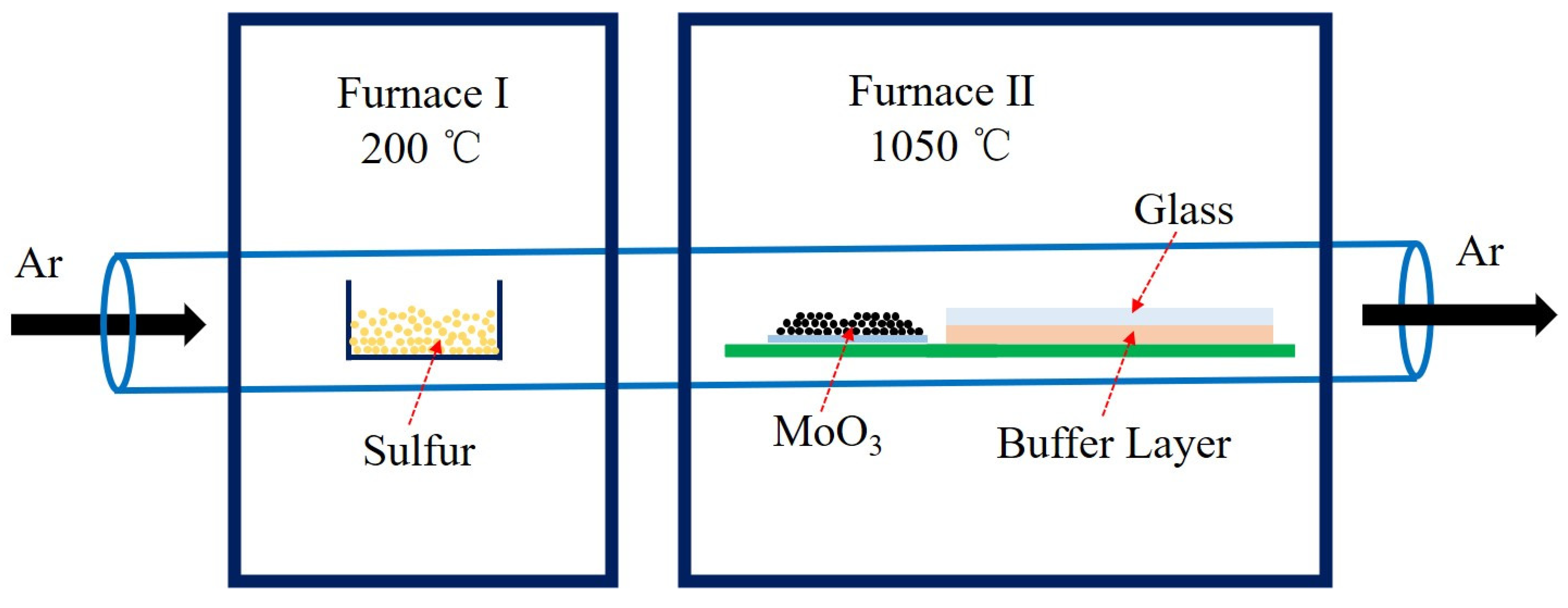
2. Experiments and Methods

As depicted in Figure 1, the MoS2 crystals were grown in a CVD system with a 2-inch-diameter quartz tube and two individual furnaces. In this system, the temperatures of substrates and precursors, carrier gas flow rate, total pressure, and the weight of precursors could be controlled independently. Following the general conditions reported in previous literature [24,25], 1.4 g of sulfur powder and 2 mg of MoO3 powder were weighed out and placed into separate boats. The boats were placed 25 cm apart in separate regions of the quartz tube to achieve the different temperatures for the S and Mo precursors. Both glass substrates and the buffer layers (Mo foils or Al2O3 lamina) were cleaned with acetone (10 min), isopropanol (10 min) and deionized water (10 min). The size of both the substrates and buffer layers was 20 mm × 20 mm. After loading precursors and substrates, the tube was first pumped down to 0.2 mBar and then filled with Ar to 1000 mBar. The pumping and filling processes were repeated three times to eliminate air and other containment gases in the quartz tube. After that, the temperatures of furnaces I and II were set to 200 and 1050 °C, respectively, with a ramping rate of 10 °C/min. During the growth, high-purity argon was loaded with a flow rate of 20 sccm. After a growth period of 10 min, the furnaces were naturally cooled to room temperature.

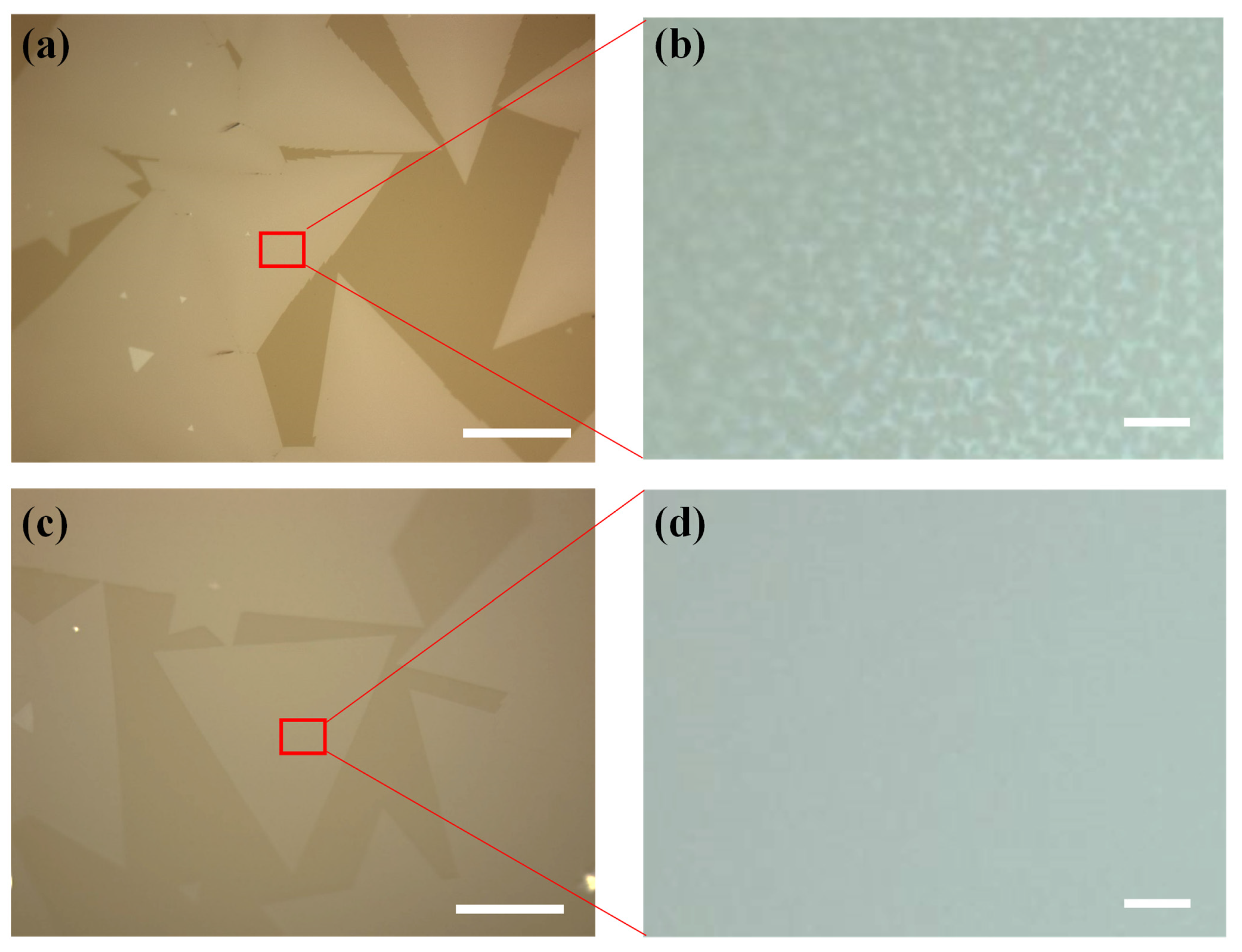
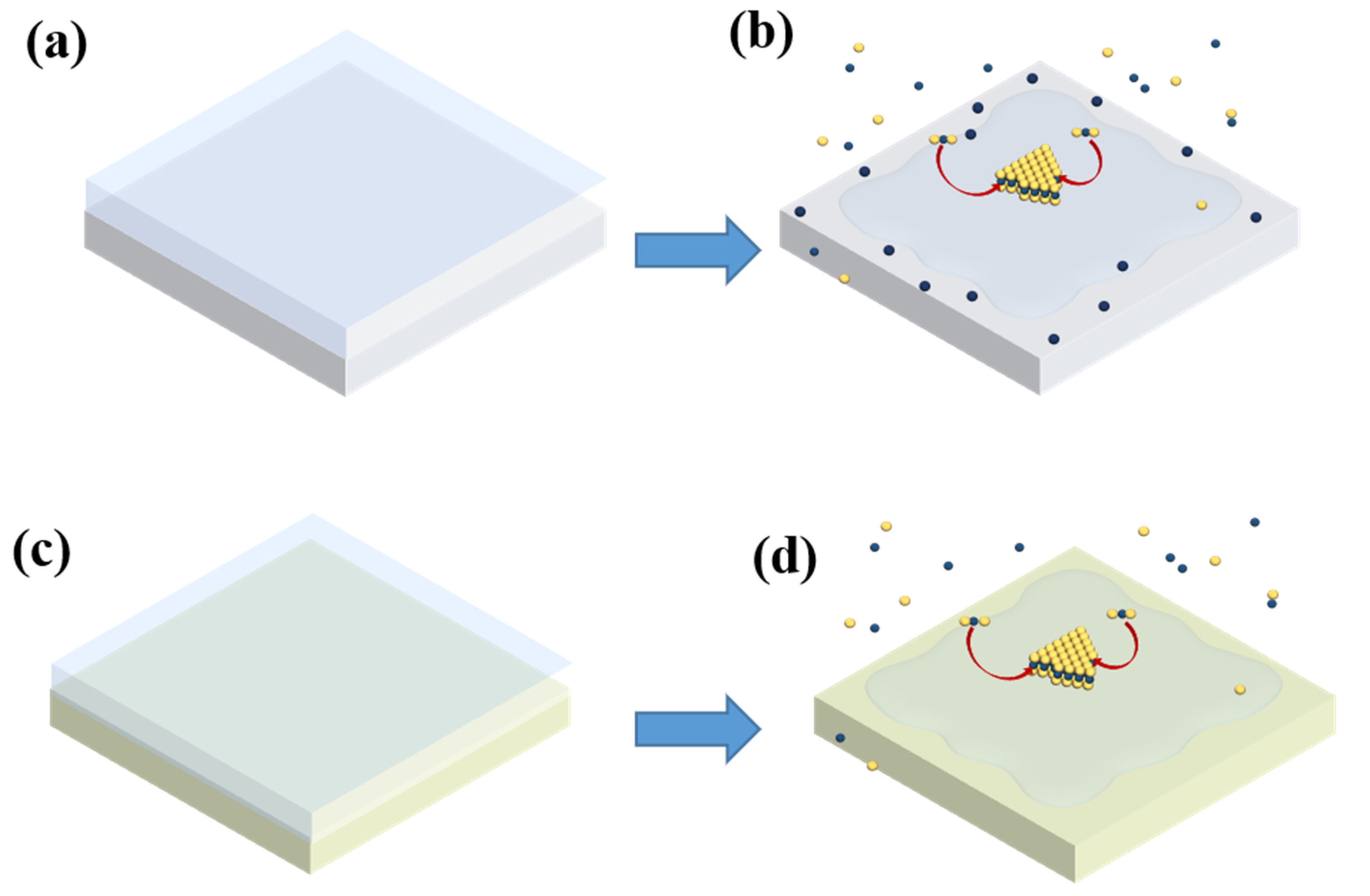
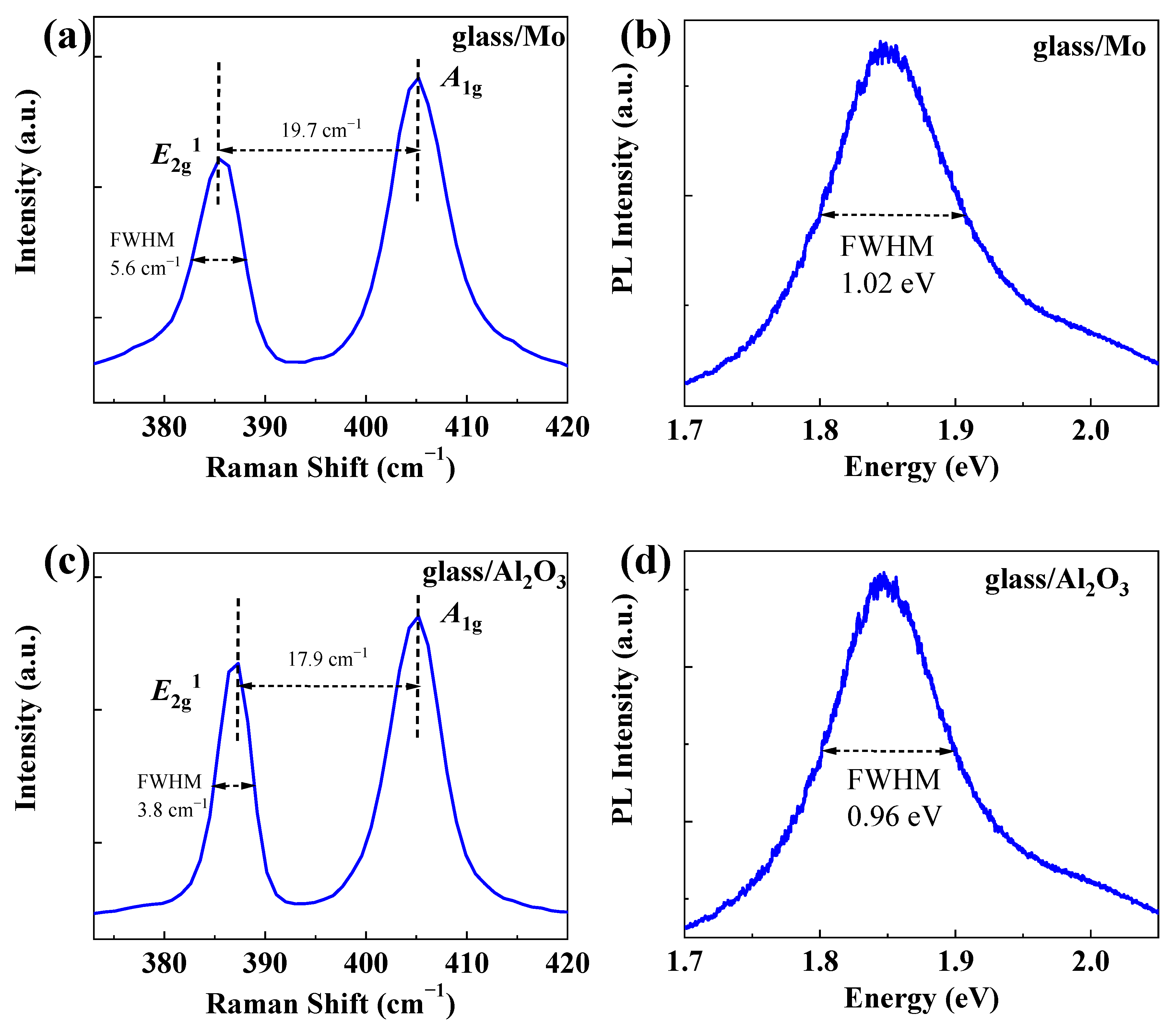
3. Results and Discussion

Figure 2a,b are the optical photographs of glass/Mo and glass/Al2O3 substrates after the growth of MoS2, respectively. The Mo foil buffer layer displays a color of gray, and the Al2O3 buffer layer shows different a color of white. Furthermore, the glass substrates shrunk obviously, and the edge of Mo foil and Al2O3 lamina showed up after the high-temperature growth process [23,26]. As we all know, the shape, distribution, and thickness of MoS2 domains depend on the weight of precursors provided to the substrates. Consequently, as illustrated in Figure 2a,b, non-uniform MoS2 film growth could be observed in different regions due to the different precursors’ concentration distributions on the glass substrates [12,33,34]. Typically, in our growth setup, thicker continuous MoS2 films could be grown upstream, closer to the Mo-source. Individual monolayer MoS2 domains tend to be synthesized downstream, farther away from the Mo-source, and abundant growth phenomena could be observed in these regions. Therefore, in order to clearly demonstrate the advantages of glass/Al2O3 substrates, the MoS2 morphology on the center and edge regions, as shown in Figure 2, was analyzed.
The MoS2 domains grown on different regions of glass/Al2O3 and glass/Mo substrates are illustrated in Figure 3 and Figure 4. Figure 3a,b are the typical optical microscopy images obtained from the MoS2 domains grown on the center region of glass/Mo substrates. The MoS2 domains exhibited triangle shapes and demonstrated lateral sizes larger than 400 μm, which is comparable to the MoS2 domain sizes on glass substrates reported in other works [12,26]. The large crystal size could be attributed to the smooth, molten surface together with the catalytic role of the glass substrates, as reported in previous works [12,26,27,35,36]. As shown in Figure 3b, numerous tiny islands could be observed on the large MoS2 triangle domains after additional magnification. The small bilayer islands could be attributed to the Mo foil buffer layer, which provides additional Mo-source during the growth of MoS2 domains. Figure 3c,d are the representative optical microscopy images obtained from the MoS2 domains grown on the center region of glass/Al2O3 substrates. Triangle MoS2 domains larger than 400 μm with uniform color contrast could be observed. In addition, no small bilayer islands could be observed on the amplified image of the MoS2 domain, which demonstrates the thickness uniformity of MoS2 crystal domains grown on the glass/Al2O3 substrates.
Figure 4 shows the MoS2 domains on the edge of the glass/Mo and the glass/Al2O3 substrates. As shown in Figure 4a, the MoS2 domains on the edge region of glass/Mo substrates generally exhibit star shapes with bright core centers. In contrast, the MoS2 domains on the edge region of glass/Al2O3 substrates are sparse and generally exhibit triangle shapes with uniform thickness, as shown in Figure 4c. In addition, both the MoS2 domains grown on glass/Mo and glass/Al2O3 were successfully transferred to SiO2/Si substrates. Figure 4b shows the transferred MoS2 domains with bright core centers that were grown on glass/Mo substrates. Figure 4d shows the transferred MoS2 domains with uniform thickness that were grown on glass/Al2O3 substrates. The details of the transfer method have been reported in our previous works [24,25,37,38].
To provide a clear explanation of the different morphologies of the MoS2 domains grown on glass/Mo and glass/Al2O3 substrates, a schematic illustration of the underlying growth mechanism was plotted. Typically, as shown in Figure 5a,b, the flat glass plane will be condensed into an oblate, sphere-like shape at a temperature higher than its molten point [23]. Subsequently, the Mo foil or Al2O3 buffer layer under glass substrates would be exposed to the CVD system. The Mo foil could be used as the Mo-source in the high-temperature CVD process, which has been demonstrated in previous work [26]. Therefore, excess Mo-source would be supplied and diffused on the glass/Mo substrates’ surface. Consequently, the MoS2 domains with small bilayer islands and bright core centers were grown at the center and edge regions, respectively. On the contrary, the strong chemical bonds of Al2O3 make it stable at high temperatures. Therefore, as shown in Figure 5c,d, the Al2O3 buffer layer would not affect the Mo-source supply during the process of MoS2 growth and MoS2 crystals with uniform thickness were grown. Furthermore, as discussed in previous works [12,26,27,35,36], the large domain size of MoS2 at the center region of glass substrates could be ascribed to the smooth, molten glass surface under high temperature, together with the catalytic role of Na in the glass substrates, which reduce the energy barrier in the CVD process.
Raman spectroscopy is one commonly used spectroscopic technique to investigate phonons as well as the vibrational, rotational and other low-frequency modes in two-dimensional materials, which could be used to provide information about both crystal quality as well as estimate the number of layers of MoS2 domains [39,40,41,42]. Therefore, Raman spectra were collected to further characterize the properties of MoS2 grown on glass/Mo and glass/Al2O3. Figure 6a,c display the Raman spectra of the transferred MoS2 domains on SiO2/Si substrates that were grown on the center regions of glass/Mo and glass/Al2O3 substrates, respectively. As shown in Figure 6a, two characteristic Raman peaks were found at 385.4 cm−1 and 405.2 cm−1 in the spectral range, which can be assigned to in-plane vibration modes of Mo and S in the opposite direction (E12g) and an out-of-plane vibration mode of S atoms (A1g). The frequency difference for the MoS2 domains grown on glass/Mo substrates was 19.7 cm−1. For the MoS2 domains grown on glass/Al2O3 substrates, the E12g and A1g peaks are located at 387.3 cm−1 and 405.2 cm−1. Compared with the MoS2 domains grown on glass/Mo substrates, the frequency difference was reduced to 17.9 cm−1, indicating a monolayer thickness for the measured MoS2 domains. Moreover, the full width at half maximum (FWHM) of the E12g peak also reduced from 5.6 cm−1 to 3.8 cm−1, demonstrating the high quality of the MoS2 domains grown on glass/Al2O3 substrates. The reduced frequency difference and FWHM results from the different morphologies of MoS2 domains grown on glass/Mo and glass/Al2O3 substrates, as shown in Figure 3. In addition, PL spectroscopy was performed for the transferred MoS2 domains grown on glass/Mo and glass/Al2O3 substrates, and the obtained spectra are shown in Figure 6b,d. Both those two types of MoS2 have a characteristic peak (A exciton peak) at 1.84 eV, which is in agreement with previous studies [24,25]. The FWHMs of the A exciton peaks for MoS2 domains grown on glass/Mo and glass/Al2O3 substrates are 1.02 and 0.96 eV, respectively. The reduced PL FWHMs of MoS2 domains grown on glass/Al2O3 could also be attributed to its uniform thickness and high crystal quality.
In order to further characterize the MoS2 domains grown on glass/Al2O3 substrates, atomic force microscopy (AFM) and Raman mapping were performed after they were transferred onto SiO2/Si substrates. Figure 7a displays the AFM images obtained from a typical triangle-shaped MoS2 domain. A thickness of 0.7 nm was demonstrated through the AFM characterization, as shown in Figure 7b. This is consistent with the thickness of the monolayer MoS2. Figure S1 displays the optical microscope and AFM images of the CVD-grown MoS2 on the center region of glass/Al2O3 substrates. As shown in Figure S1b, numerous tiny islands could be observed on the large MoS2 triangle domains. Figure 7c,d show the Raman intensity mappings recorded at 387.3 cm−1 and 405.2 cm−1, respectively. The Raman mappings on the intensity of E12g mode and A1g mode reveal a uniform color contrast, further demonstrating the thickness uniformity and good crystallinity of MoS2 grown on glass/Al2O3 substrates.

4. Conclusions

In this work, the two-dimensional semiconductor MoS2 was successfully synthesized on glass/Al2O3 substrates for the first time. The advantages of glass/Al2O3 substrates for CVD MoS2 growth were demonstrated by a direct comparison of glass/Mo substrates. Optical microscopy revealed that MoS2 crystals grown on both glass/Mo and glass/Al2O3 substrates were conventionally triangle-shaped and had a lateral size larger than 400 μm. Numerous bilayer islands and bright core centers could be observed on the surface of MoS2 domains at the center region and edge region of glass/Mo substrates. As a control, MoS2 domains grown on glass/Al2O3 substrates exhibited uniform optical contrast, demonstrating the thickness uniformity of those MoS2 domains. The Raman and PL comparison of MoS2 domains further confirmed this. In addition, the thickness of MoS2 domains was characterized by atomic force microscopy and the homogeneity of MoS2 domains grown on glass/Al2O3 substrates was further demonstrated by Raman mapping. These results demonstrate a novel method to produce MoS2 films on glass substrates and are of great value for future commercial applications of MoS2 films.

Supplementary Materials

The following supporting information can be downloaded at: https://www.mdpi.com/article/10.3390/nano12152719/s1, Figure S1: AFM image of the CVD growth MoS2 on glass/Mo substrates.

Author Contributions

Conceptualization, Q.G.; methodology, Q.G., J.L., L.C., Z.X. and S.C.; validation, Q.G. and S.C.; formal analysis, Q.G.; investigation, Q.G., S.C. and L.C.; resources, Q.G., P.L., X.Z. and W.C.; data curation, Q.G.; writing—original draft preparation, Q.G.; writing—review and editing, Q.G.; visualization, Q.G., D.L. and S.X.; supervision, Q.G.; project administration, Q.G. and C.Z.; funding acquisition, Q.G. and C.Z. All authors have read and agreed to the published version of the manuscript.

Funding

This work was funded in part by the Natural Science Foundation of China (Grant Nos. 62104033, 62071088 and 11775047), in part by the Guangdong Basic and Applied Basic Research Foundation (Grant No. 2019A1515110752), in part by the Youth Innovative Talent Project of Guangdong Education Department (Grant No. 2019KQNCX187), in part by the Outstanding Chinese and Foreign Youth Exchange Program of China Association for Science and Technology (CAST) 2019, in part by the Project for Innovation Team of Guangdong University (Grant Nos. 2018KCXTD033, 2020KCXTD030 and 2021KCXTD040), in part by the Construction Project of Professional Quality Engineering in 2022 (Grant No. YLZY202201), in part by the key scientific research project of the Department of Education of Guangdong Province (Grant No. 2021ZDZX1052), and in part by National Key R&D Program of China (Grant No. 2018YFB1801302).

Data Availability Statement

The data that support the findings of this study are available from the corresponding author upon reasonable request.

Conflicts of Interest

The authors declare no conflict of interest.

References

  1. Wu, F.; Tian, H.; Shen, Y.; Hou, Z.; Ren, J.; Gou, G.; Sun, Y.; Yang, Y.; Ren, T.-L. Vertical MoS2 transistors with sub-1-nm gate lengths. Nature 2022, 603, 259–264. [Google Scholar] [CrossRef] [PubMed]
  2. Shen, P.-C.; Su, C.; Lin, Y.; Chou, A.-S.; Cheng, C.-C.; Park, J.-H.; Chiu, M.-H.; Lu, A.-Y.; Tang, H.-L.; Tavakoli, M.M.; et al. Ultralow contact resistance between semimetal and monolayer semiconductors. Nature 2021, 593, 211–217. [Google Scholar] [CrossRef]
  3. Meng, W.; Xu, F.; Yu, Z.; Tao, T.; Shao, L.; Liu, L.; Li, T.; Wen, K.; Wang, J.; He, L.; et al. Three-dimensional monolithic micro-LED display driven by atomically thin transistor matrix. Nat. Nanotechnol. 2021, 16, 1231–1236. [Google Scholar] [CrossRef] [PubMed]
  4. Zhang, X.; Grajal, J.; Vazquez-Roy, J.L.; Radhakrishna, U.; Wang, X.; Chern, W.; Zhou, L.; Lin, Y.; Shen, P.-C.; Ji, X.; et al. Two-dimensional MoS2-enabled flexible rectenna for Wi-Fi-band wireless energy harvesting. Nature 2019, 566, 368–372. [Google Scholar] [CrossRef] [PubMed]
  5. Lin, Z.; Liu, Y.; Halim, U.; Ding, M.; Liu, Y.; Wang, Y.; Jia, C.; Chen, P.; Duan, X.; Wang, C.; et al. Solution-processable 2D semiconductors for high-performance large-area electronics. Nature 2018, 562, 254–258. [Google Scholar] [CrossRef] [PubMed]
  6. Desai, S.B.; Madhvapathy, S.R.; Sachid, A.B.; Llinas, J.P.; Wang, Q.; Ahn, G.H.; Pitner, G.; Kim, M.J.; Bokor, J.; Hu, C.; et al. MoS 2 transistors with 1-nanometer gate lengths. Science 2016, 354, 99–102. [Google Scholar] [CrossRef] [Green Version]
  7. Akinwande, D.; Petrone, N.; Hone, J. Two-dimensional flexible nanoelectronics. Nat. Commun. 2014, 5, 5678. [Google Scholar] [CrossRef]
  8. Li, T.; Guo, W.; Ma, L.; Li, W.; Yu, Z.; Han, Z.; Gao, S.; Liu, L.; Fan, D.; Wang, Z.; et al. Epitaxial growth of wafer-scale molybdenum disulfide semiconductor single crystals on sapphire. Nat. Nanotechnol. 2021, 16, 1201–1207. [Google Scholar] [CrossRef]
  9. Liu, L.; Li, T.; Ma, L.; Li, W.; Gao, S.; Sun, W.; Dong, R.; Zou, X.; Fan, D.; Shao, L.; et al. Uniform nucleation and epitaxy of bilayer molybdenum disulfide on sapphire. Nature 2022, 605, 69–75. [Google Scholar] [CrossRef]
  10. Yang, P.; Zhang, S.; Pan, S.; Tang, B.; Liang, Y.; Zhao, X.; Zhang, Z.; Shi, J.; Huan, Y.; Shi, Y.; et al. Epitaxial Growth of Centimeter-Scale Single-Crystal MoS2 Monolayer on Au(111). ACS Nano 2020, 14, 5036–5045. [Google Scholar] [CrossRef]
  11. Wang, Q.; Li, N.; Tang, J.; Zhu, J.; Zhang, Q.; Jia, Q.; Lu, Y.; Wei, Z.; Yu, H.; Zhao, Y.; et al. Wafer-Scale Highly Oriented Monolayer MoS2 with Large Domain Sizes. Nano Lett. 2020, 20, 7193–7199. [Google Scholar] [CrossRef] [PubMed]
  12. Yang, P.; Zou, X.; Zhang, Z.; Zhongfan, L.; Shi, J.; Chen, S.; Shulin, C.; Zhao, L.; Jiang, S.; Zhou, X.; et al. Batch production of 6-inch uniform monolayer molybdenum disulfide catalyzed by sodium in glass. Nat. Commun. 2018, 9, 979. [Google Scholar] [CrossRef] [PubMed]
  13. Yu, H.; Liao, M.; Zhao, W.; Liu, G.; Zhou, X.J.; Wei, Z.; Xu, X.; Liu, K.; Hu, Z.; Deng, K.; et al. Wafer-Scale Growth and Transfer of Highly-Oriented Monolayer MoS2 Continuous Films. ACS Nano 2017, 11, 12001–12007. [Google Scholar] [CrossRef]
  14. Zhou, J.; Lin, J.; Huang, X.; Zhou, Y.; Chen, Y.; Xia, J.; Wang, H.; Xie, Y.; Yu, H.; Lei, J.; et al. A library of atomically thin metal chalcogenides. Nature 2018, 556, 355–359. [Google Scholar] [CrossRef] [PubMed]
  15. Ji, Q.; Su, C.; Mao, N.; Tian, X.; Idrobo, J.-C.; Miao, J.; Tisdale, W.A.; Zettl, A.; Li, J.; Kong, J. Revealing the Brønsted-Evans-Polanyi relation in halide-activated fast MoS2 growth toward millimeter-sized 2D crystals. Sci. Adv. 2021, 7, eabj3274. [Google Scholar] [CrossRef] [PubMed]
  16. Zhang, L.; Dong, J.; Ding, F. Strategies, Status, and Challenges in Wafer Scale Single Crystalline Two-Dimensional Materials Synthesis. Chem. Rev. 2021, 121, 6321–6372. [Google Scholar] [CrossRef] [PubMed]
  17. Li, S. Salt-assisted chemical vapor deposition of two-dimensional transition metal dichalcogenides. iScience 2021, 24, 103229. [Google Scholar] [CrossRef]
  18. Zhou, S.; Jiao, L. Growth of Single-crystalline Transition Metal Dichalcogenides Monolayers with Large-size. Chem. Res. Chin. Univ. 2020, 36, 511–517. [Google Scholar] [CrossRef]
  19. Xu, X.; Zhang, Z.; Qiu, L.; Zhuang, J.; Zhang, L.; Wang, H.; Liao, C.; Song, H.; Qiao, R.; Gao, P.; et al. Ultrafast growth of single-crystal graphene assisted by a continuous oxygen supply. Nat. Nanotechnol. 2016, 11, 930–935. [Google Scholar] [CrossRef]
  20. Zhang, Z.; Xu, X.; Qiu, L.; Wang, S.; Wu, T.; Ding, F.; Peng, H.; Liu, K. The Way towards Ultrafast Growth of Single-Crystal Graphene on Copper. Adv. Sci. 2017, 4, 1700087. [Google Scholar] [CrossRef] [Green Version]
  21. Xiong, L.; Wang, K.; Li, D.; Luo, X.; Weng, J.; Liu, Z.; Zhang, H. Research progress on the preparations, characterizations and applications of large scale 2D transition metal dichalcogenides films. FlatChem 2020, 21, 100161. [Google Scholar] [CrossRef]
  22. Li, Q.; Zhang, L.; Li, C.; He, J.; Wei, Y.; Zhao, J.; Zhang, R.; Wang, P.; Fu, S.; Chen, F.; et al. Morphological Evolution of Monolayer MoS2 Single-Crystalline Flakes. J. Phys. Chem. C 2022, 126, 3549–3559. [Google Scholar] [CrossRef]
  23. Zeng, M.; Liu, J.; Zhou, L.; Mendes, R.G.; Dong, Y.; Zhang, M.-Y.; Cui, Z.-H.; Cai, Z.; Zhang, Z.; Zhu, D.; et al. Bandgap tuning of two-dimensional materials by sphere diameter engineering. Nat. Mater. 2020, 19, 528–533. [Google Scholar] [CrossRef] [PubMed]
  24. Zhang, Z.; Xu, X.; Song, J.; Gao, Q.; Li, S.; Hu, Q.; Li, X.; Wu, Y. High-performance transistors based on monolayer CVD MoS2 grown on molten glass. Appl. Phys. Lett. 2018, 113, 202103. [Google Scholar] [CrossRef]
  25. Gao, Q.; Zhang, Z.; Xu, X.; Song, J.; Li, X.; Wu, Y. Scalable high performance radio frequency electronics based on large domain bilayer MoS2. Nat. Commun. 2018, 9, 4778. [Google Scholar] [CrossRef]
  26. Chen, J.; Zhao, X.; Grinblat, G.; Chen, Z.; Tan, S.J.R.; Fu, W.; Ding, Z.; Abdelwahab, I.; Li, Y.; Geng, D.; et al. Homoepitaxial Growth of Large-Scale Highly Organized Transition Metal Dichalcogenide Patterns. Adv. Mater. 2017, 30, 1704674. [Google Scholar] [CrossRef] [PubMed]
  27. Chen, J.; Zhao, X.; Tan, S.J.R.; Xu, H.; Wu, B.; Liu, B.; Fu, D.; Fu, W.; Geng, D.; Liu, Y.; et al. Chemical Vapor Deposition of Large-Size Monolayer MoSe2 Crystals on Molten Glass. J. Am. Chem. Soc. 2017, 139, 1073–1076. [Google Scholar] [CrossRef]
  28. Cai, Z.; Lai, Y.; Zhao, S.; Zhang, R.; Tan, J.; Feng, S.; Zou, J.; Tang, L.; Lin, J.; Liu, B.; et al. Dissolution-precipitation growth of uniform and clean two dimensional transition metal dichalcogenides. Natl. Sci. Rev. 2020, 8, 115. [Google Scholar] [CrossRef]
  29. Tang, J.; Wei, Z.; Wang, Q.; Wang, Y.; Han, B.; Li, X.; Huang, B.; Liao, M.; Liu, J.; Li, N.; et al. In Situ Oxygen Doping of Monolayer MoS 2 for Novel Electronics. Small 2020, 16, 2004276. [Google Scholar] [CrossRef]
  30. Durairaj, S.; Ponnusamy, K.; Shinde, N.B.; Eswaran, S.K.; Asokan, V.; Park, J.B.; Chandramohan, S. Oxygen-Driven Growth Regulation and Defect Passivation in Chemical Vapor Deposited MoS2 Monolayers. Cryst. Growth Des. 2021, 21, 6793–6801. [Google Scholar] [CrossRef]
  31. Yao, B.; Li, R.; Zhang, C.; Zhou, Z.; Fu, Z.; Huang, X.; Yuan, G.; Xu, J.; Gao, L. Tuning the morphology of 2D transition metal chalcogenides via oxidizing conditions. J. Physics Condens. Matter 2022, 34, 195001. [Google Scholar] [CrossRef] [PubMed]
  32. Chen, W.; Zhao, J.; Zhang, J.; Gu, L.; Yang, Z.; Li, X.; Yu, H.; Zhu, X.; Yang, R.; Shi, D.; et al. Oxygen-Assisted Chemical Vapor Deposition Growth of Large Single-Crystal and High-Quality Monolayer MoS2. J. Am. Chem. Soc. 2015, 137, 15632–15635. [Google Scholar] [CrossRef] [PubMed]
  33. Tang, L.; Li, T.; Luo, Y.; Feng, S.; Cai, Z.; Zhang, H.; Liu, B.; Cheng, H.-M. Vertical Chemical Vapor Deposition Growth of Highly Uniform 2D Transition Metal Dichalcogenides. ACS Nano 2020, 14, 4646–4653. [Google Scholar] [CrossRef]
  34. Tang, L.; Tan, J.; Nong, H.; Liu, B.; Cheng, H.-M. Chemical Vapor Deposition Growth of Two-Dimensional Compound Materials: Controllability, Material Quality, and Growth Mechanism. Accounts Mater. Res. 2021, 2, 36–47. [Google Scholar] [CrossRef]
  35. Zhang, Z.; Zhu, L.; Wang, D.; Tang, B.; Yang, P.; Shi, Y.; Zhou, F.; Fu, J.; Huan, Y.; Cui, F.; et al. Ultrafast Growth of Large-Area Uniform, Millimeter-Size MoSe 2 Single Crystals on Low-Cost Soda-Lime Glass. Adv. Mater. Interfaces 2021, 8, 2100415. [Google Scholar] [CrossRef]
  36. Han, W.; Liu, K.; Yang, S.; Wang, F.; Su, J.; Jin, B.; Li, H.; Zhai, T. Salt-assisted chemical vapor deposition of two-dimensional materials. Sci. China Ser. B Chem. 2019, 62, 1300–1311. [Google Scholar] [CrossRef]
  37. Gao, Q.; Zhang, C.; Yang, K.; Pan, X.; Zhang, Z.; Yang, J.; Yi, Z.; Chi, F.; Liu, L. High-Performance CVD Bilayer MoS2 Radio Frequency Transistors and Gigahertz Mixers for Flexible Nanoelectronics. Micromachines 2021, 12, 451. [Google Scholar] [CrossRef]
  38. Gao, Q.; Zhang, C.; Liu, P.; Hu, Y.; Yang, K.; Yi, Z.; Liu, L.; Pan, X.; Zhang, Z.; Yang, J.; et al. Effect of Back-Gate Voltage on the High-Frequency Performance of Dual-Gate MoS2 Transistors. Nanomaterials 2021, 11, 1594. [Google Scholar] [CrossRef]
  39. Wang, Y.; Cong, C.; Qiu, C.; Yu, T. Raman Spectroscopy Study of Lattice Vibration and Crystallographic Orientation of Monolayer MoS2under Uniaxial Strain. Small 2013, 9, 2857–2861. [Google Scholar] [CrossRef]
  40. Li, H.; Zhang, Q.; Yap, C.C.R.; Tay, B.K.; Edwin, T.H.T.; Olivier, A.; Baillargeat, D. From Bulk to Monolayer MoS2: Evolution of Raman Scattering. Adv. Funct. Mater. 2012, 22, 1385–1390. [Google Scholar] [CrossRef]
  41. Chakraborty, B.; Bera, A.; Muthu, D.V.S.; Bhowmick, S.; Waghmare, U.V.; Sood, A.K. Symmetry-dependent phonon renormalization in monolayer MoS22transistor. Phys. Rev. B 2012, 85, 161403. [Google Scholar] [CrossRef] [Green Version]
  42. Zobel, A.; Boson, A.; Wilson, P.M.; Muratov, D.S.; Kuznetsov, D.V.; Sinitskii, A. Chemical vapour deposition and characterization of uniform bilayer and trilayer MoS2crystals. J. Mater. Chem. C 2016, 4, 11081–11087. [Google Scholar] [CrossRef]
Figure 1. Schematic illustration of the CVD growth system setup.
Nanomaterials 12 02719 g001
Figure 2. (a) Optical photograph of the glass/Mo substrates after the growth of MoS2. (b) Optical photograph of the glass/Al2O3 substrates after the growth of MoS2. The red rectangle corresponds to the center region, and the blue rectangle corresponds to the edge region.
Nanomaterials 12 02719 g002
Figure 3. (a,b) Optical microscope images of the MoS2 domains synthesized on the center region of glass/Mo substrates. (c,d) Optical microscope images of the MoS2 domains synthesized on the center region of glass/Al2O3 substrates. Scale bar represents 200 μm for (a,c), and 10 μm for (b,d).
Nanomaterials 12 02719 g003
Figure 4. (a,b) Optical microscope images of the MoS2 domains synthesized on the edge region of glass/Mo substrates. (c,d) Optical microscope images of the MoS2 domains synthesized on the edge region of glass/Al2O3 substrates. Scale bar represents 50 μm for (ad).
Nanomaterials 12 02719 g004
Figure 5. (a,b) Schematic illustration of the CVD growth process on glass/Mo substrates. (c,d) Schematic illustration of the CVD growth process on glass/Al2O3 substrates. The blue balls and yellow balls in (b,d) represent Mo and S atoms, respectively.
Nanomaterials 12 02719 g005
Figure 6. (a,b) Raman and PL spectral of the CVD-grown MoS2 on the center region of glass/Mo substrates. (c,d) Raman and PL spectral of the CVD-grown MoS2 on the center region of glass/Al2O3 substrates.
Nanomaterials 12 02719 g006
Figure 7. (a,b) AFM image and height profile of the CVD-grown MoS2 on glass/Al2O3 substrates. (c,d) Raman mapping of the CVD-grown MoS2 on glass/Al2O3 substrates. Scale bar are 5 μm for (a), and Scale bars are 3 μm for (c,d).
Nanomaterials 12 02719 g007
Publisher’s Note: MDPI stays neutral with regard to jurisdictional claims in published maps and institutional affiliations.

